Recent Developments in the Field of the Metal-Insulator Transition in Two Dimensions

1
Institute of Solid State Physics, Chernogolovka, 142432 Moscow District, Russia
2
Physics Department, Northeastern University, Boston, MA 02115, USA
*
Author to whom correspondence should be addressed.
Appl. Sci. 2019, 9(6), 1169; https://doi.org/10.3390/app9061169
Submission received: 27 November 2018
/
Revised: 10 March 2019
/
Accepted: 14 March 2019
/
Published: 19 March 2019
(This article belongs to the Special Issue Metal-Insulator Transitions)
Abstract
:We review the latest developments in the field of the metal-insulator transition in strongly-correlated two-dimensional electron systems. Particular attention is given to recent discoveries of a sliding quantum electron solid and interaction-induced spectrum flattening at the Fermi level in high-quality silicon-based structures.
1. Introduction
The zero-magnetic-field metal-insulator transition (MIT) was discovered in a strongly-interacting two-dimensional (2D) electron system in silicon metal-oxide-semiconductor field-effect transistors (MOSFETs) [1,2,3] and later reported in a wide variety of 2D electron and hole systems: p-type SiGe heterostructures, p- and n-type GaAs/AlGaAs heterostructures, AlAs heterostructures, ZnO-related heterostructures, etc. (for reviews, see [4,5,6,7]). The strongest drop of the resistance on the metallic side of the transition (up to a factor of 12) at sub-Kelvin temperatures was reported in 2D systems in SiGe/Si/SiGe quantum wells [8]; in spite of lower disorder, the drop of the resistance in GaAs-based structures never exceeded a factor of about three. This discrepancy has been attributed particularly to the fact that electrons in silicon-based structures have two almost degenerate valleys, which further enhances the correlation effects [9,10].
Here, we briefly review the experimental data obtained in different strongly-correlated 2D electron and hole systems in zero and non-zero magnetic fields on both sides of the metal-insulator transition; the term strongly correlated means that the interaction parameter given by the ratio of the Coulomb and Fermi energies, , exceeds (here, is the valley degeneracy, is the areal density of carriers, and is the effective Bohr radius in the semiconductor). Then, we will discuss the behavior of the effective electron mass and the Landé g-factor on the metallic side of the transition. Finally, transport evidence for the formation of a quantum electron solid on the insulating side of the transition will be reviewed.
2. Metal-Insulator Transition in Zero Magnetic Field
The existence of a metallic state at zero magnetic field in 2D was first predicted by Finkelstein [11,12] and Castellani et al. [13]. The combined effects of interactions and disorder were studied by perturbative renormalization group methods. The possibility of metallic behavior was confirmed later in [9,10,14].
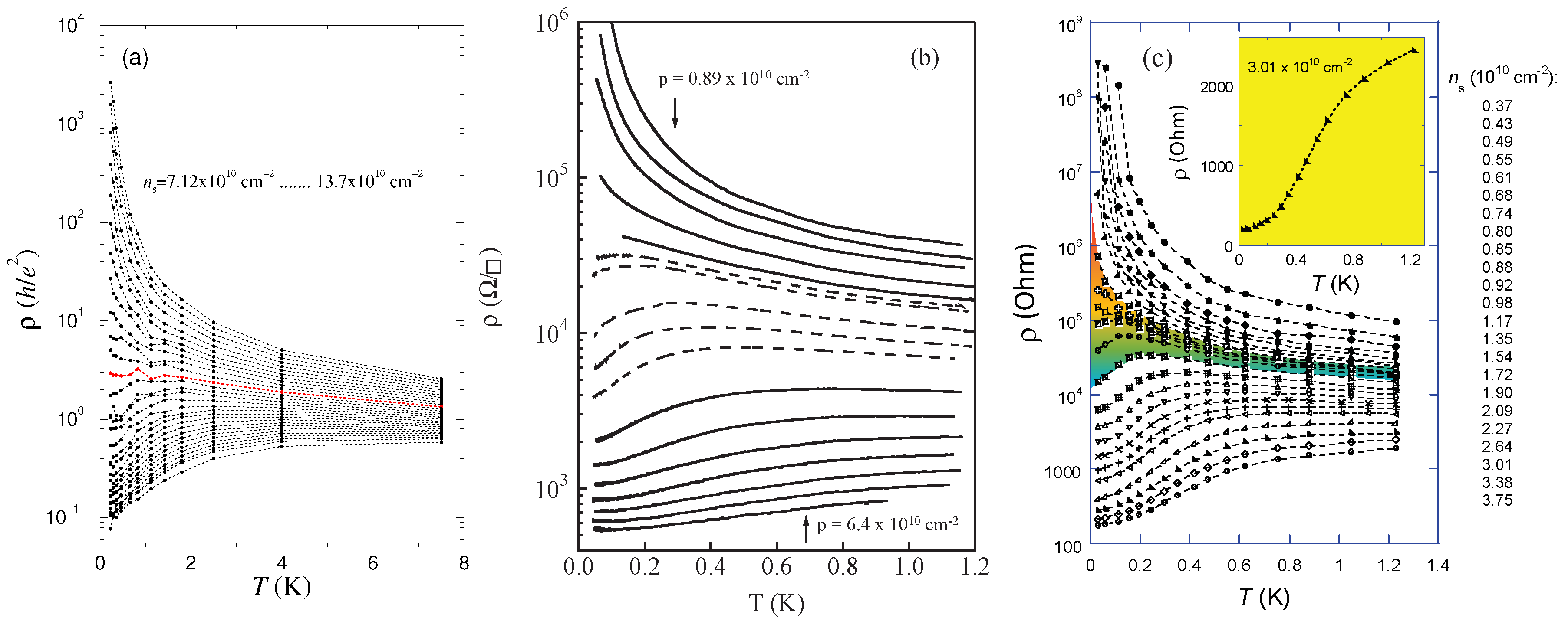
Typical experimental data showing the resistivity as a function of temperature T for different electron densities in various systems are presented in Figure 1 [8,15,16]. At the lowest temperatures, the resistivity exhibits a strong metallic temperature dependence () for electron densities above a well-defined critical value, , and insulating behavior () for . One refers to the regime at as metallic and to that at as insulating [17]. The two regimes are separated by a separatrix, indicated in Figure 1a by a dotted red line. This curve is often tilted in agreement with [10], but becomes flat in the low-temperature limit or over an extended temperature range in the most uniform samples [18]. The dependences on the metallic side of the transition at just above are non-monotonic; while at temperatures exceeding a density-dependent value , the derivative is negative; it changes sign at temperatures below .
However, to determine the critical density for the MIT, one cannot rely on the derivative criterion alone. In [17], an additional method was used based on vanishing activation energy and the vanishing nonlinearity of the current-voltage characteristics (looking from the insulating side of the transition). It was shown that in clean Si MOSFETs in zero magnetic field, the critical density , determined by such a method, coincides with the critical density determined by the derivative criterion.
3. Influence of the Magnetic Field Parallel to the 2D Plane
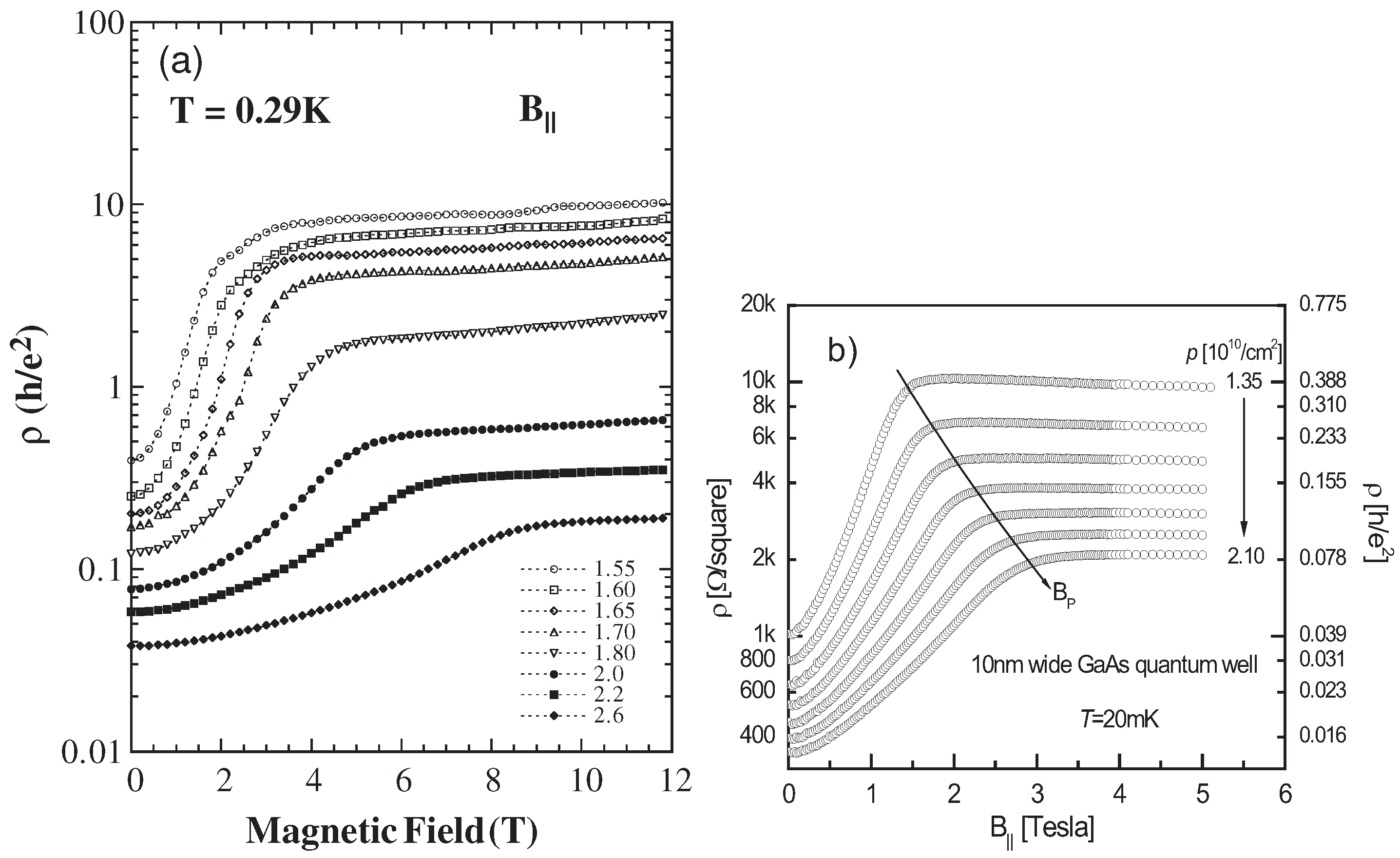
The magnetoresistance in magnetic fields parallel to the 2D plane is strong and positive [19,20,21] (examples are shown in Figure 2), but eventually saturates above some density-dependent magnetic field . In sufficiently-thin quantum wells, has little effect on the orbital motion of the electrons and couples only to the electron spin; therefore, it is reasonable to attribute the saturation of the magnetoresistance to the complete spin polarization of the electron system [22]. Indeed, from the analysis of the positions of Shubnikov–de Haas oscillations in tilted magnetic fields [23,24], it was concluded that the magnetic field is equal to that required to polarize the electrons’ spins fully.
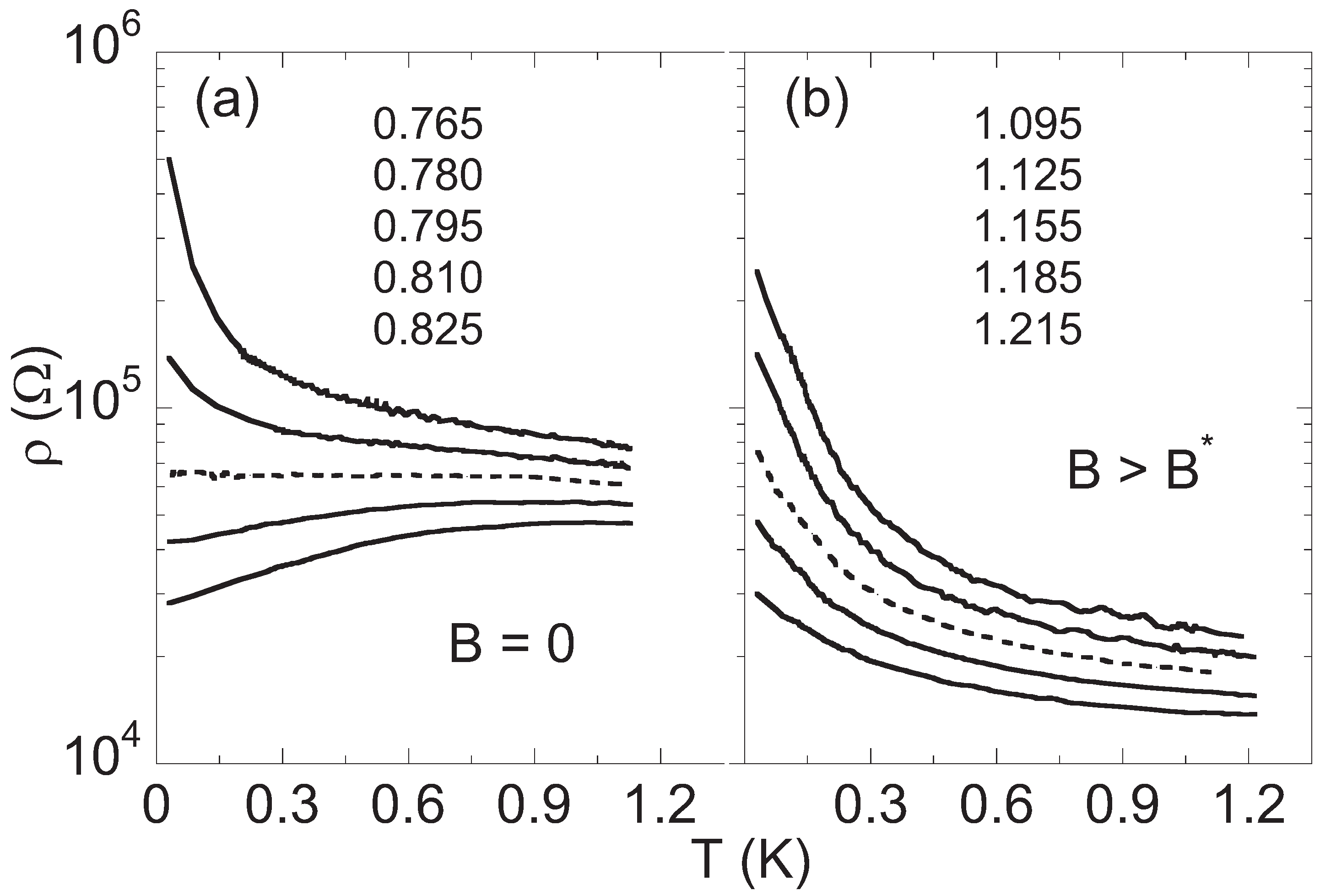
Another effect of the parallel magnetic field is that it wipes out the strong metallic temperature dependence of the resistance at electron densities just above and suppresses the metallic regime [7,17,19,25,26,27]. In Figure 3, the temperature dependences of the resistivity in zero magnetic field (Figure 3a) are compared with those measured in a parallel magnetic field, Tesla, high enough to cause full spin polarization (Figure 3b). The dashed (middle) curves on both panels correspond to the critical electron densities, , determined by the method of vanishing activation energy and vanishing nonlinearity of the current-voltage characteristics outlined above. The middle curve in Figure 3a, corresponding to , is flat below 1 K. In sharp contrast with the situation, at , not only are the curves non-symmetric about the middle curve corresponding to , but all of them have negative “insulating-like” derivatives in the entire temperature range, although the values of the resistivity are comparable to those in the case. Moreover, in a strong parallel magnetic field, there is no temperature-independent curve at any electron density [17]. Concerning the suppression of the metallic regime, it has been shown that the parallel magnetic field-induced increase in the critical electron density by the factor of about 1.4, observed in a strongly-interacting two-dimensional electron system, is caused by the effects of exchange and correlations [26].
4. Spin Susceptibility; g-Factor; the Effective Mass
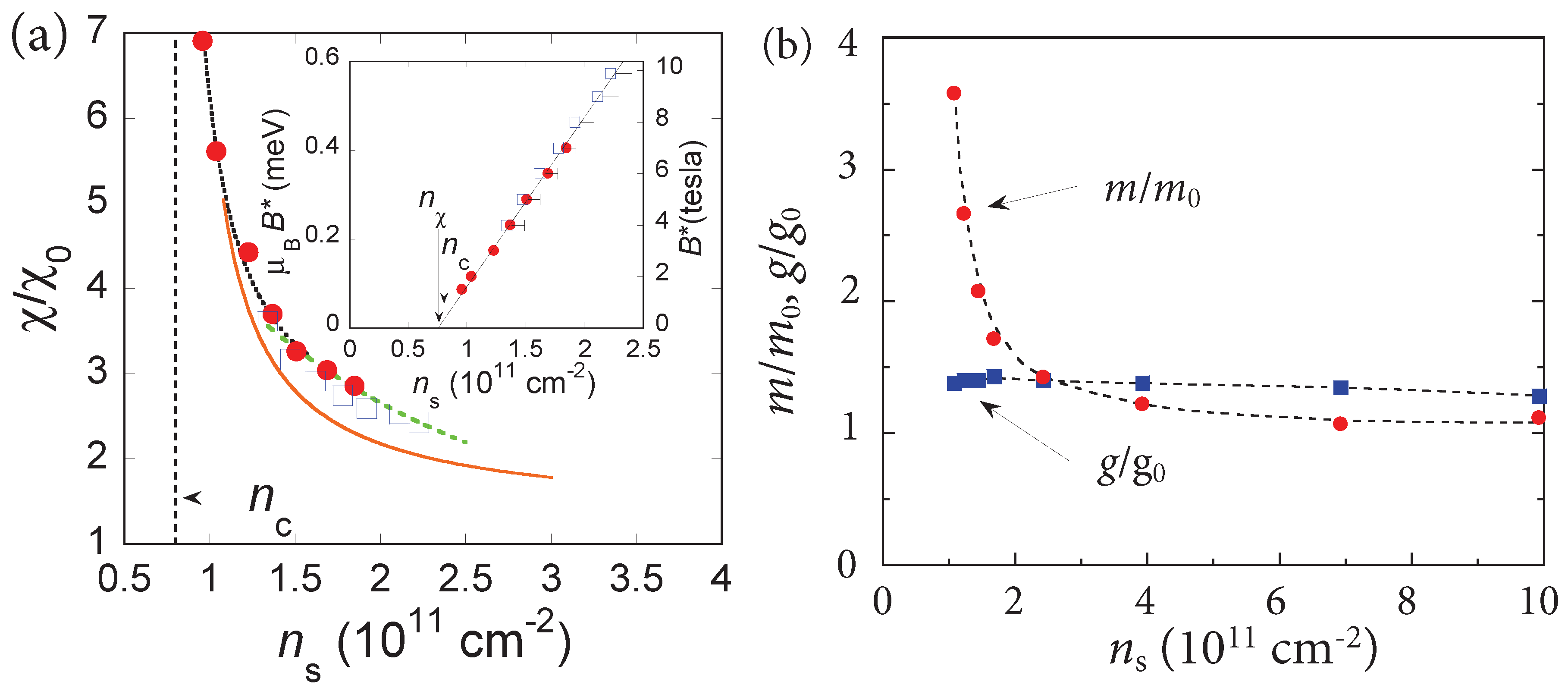
In [28], the Shubnikov–de Haas oscillations in a 2D electron system in silicon were studied at low electron densities, and it was shown that near the metal-insulator transition, only “spin” minima of the resistance at Landau-level filling factors 2, 6, 10, and 14 are seen, while the “cyclotron” minima at 4, 8, and 12 disappear. A simple explanation of the observed behavior requires a giant enhancement of the ratio between the spin and cyclotron splittings near the metal-insulator transition. Indeed, it turned out that with decreasing electron density (increasing interaction strength), the Pauli spin susceptibility, , measured by several independent methods [29,30], grows by as much as a factor of seven compared to its non-interacting value, , with a tendency to diverge at a disorder-independent density (see Figure 4a). A similar increase of the spin susceptibility near the metal-insulator transition has been observed in single-crystalline ZnO-based heterostructures [31].
In principle, this behavior can be due to either the increase of the effective electron mass or that of the Landé g-factor (or both). In [32], these two values have been measured separately, and it has been shown that the dramatic increase of the spin susceptibility is due to the strongly-enhanced effective mass, while the g-factor remains almost constant and close to its value in bulk silicon (see Figure 4b). The strong increase of the effective mass has been later independently confirmed by the analysis of the temperature dependence of Shubnikov–de Haas oscillations [33] and magnetization measurements in perpendicular magnetic fields [34].
In measurements of the thermopower in Si MOSFETs, data obtained for electron densities that are much closer to the critical point than the earlier measurements confirm that the critical density lies close to, but is consistently below the critical density for the MIT [35]. The results indicate the occurrence of an interaction-induced transition to a new phase at low density that may be a precursor phase or a direct transition to the Wigner solid.
It has been found recently that in contrast to previous experiments on lower-mobility samples, in ultra-high mobility SiGe/Si/SiGe quantum wells, the critical electron density of the MIT becomes smaller than the density , where the effective mass at the Fermi level tends to diverge [8].
5. Band Flattening: Possible Condensation of Fermions
The creation and investigation of flat-band materials is a forefront area of modern condensed matter physics [36,37,38,39]. In particular, the interest is ignited by the fact that, due to the anomalous density of states, the flattening of the band may be important for the construction of room temperature superconductivity. The appearance of a flat band is theoretically predicted [40,41,42] in a number of systems including high-temperature superconductors, heavy fermion systems, He, and 2D electron systems. As the strength of fermion–fermion interaction is increased, the single-particle spectrum becomes progressively flatter in the vicinity of the Fermi energy, eventually forming a plateau. The flattening of the spectrum is related to the increase of the effective fermion mass at the Fermi level and the corresponding peak in the density of states.
The experimental data obtained in strongly-correlated 2D electron systems can be divided into two groups:
- (a)
- data describing the electron system as a whole, like thermodynamic density of states, magnetization of the electron system, or the magnetic field required to polarize electron spins fully and
- (b)
- data related only to the electrons at the Fermi level, like the amplitude of the Shubnikov–de Haas oscillations. This yields the effective mass and Landé g-factor at the Fermi level.
Usually, the data in the first group are interpreted using the language of quasiparticles, in which the energy-averaged effective mass, m, and Landé g-factor, g, are used. To determine the values, the formulas that hold for the case of non-interacting electrons are used. Although this approach is ideologically not correct, the results for m and g are often the same as, or close to, the results for and . For example, the simultaneous increase of the energy-averaged effective mass and that at the Fermi level in Si MOSFETs was reported in publications described in the previous section.
In [43], the magnetic field required to polarize the electrons’ spins fully in the ultra-high mobility 2D electron system in SiGe/Si/SiGe quantum wells of unprecedented quality [44] has been investigated. The product that characterizes the whole 2D electron system can be determined in the clean limit from the equality of the Zeeman splitting and the Fermi energy of the spin-polarized electron system:
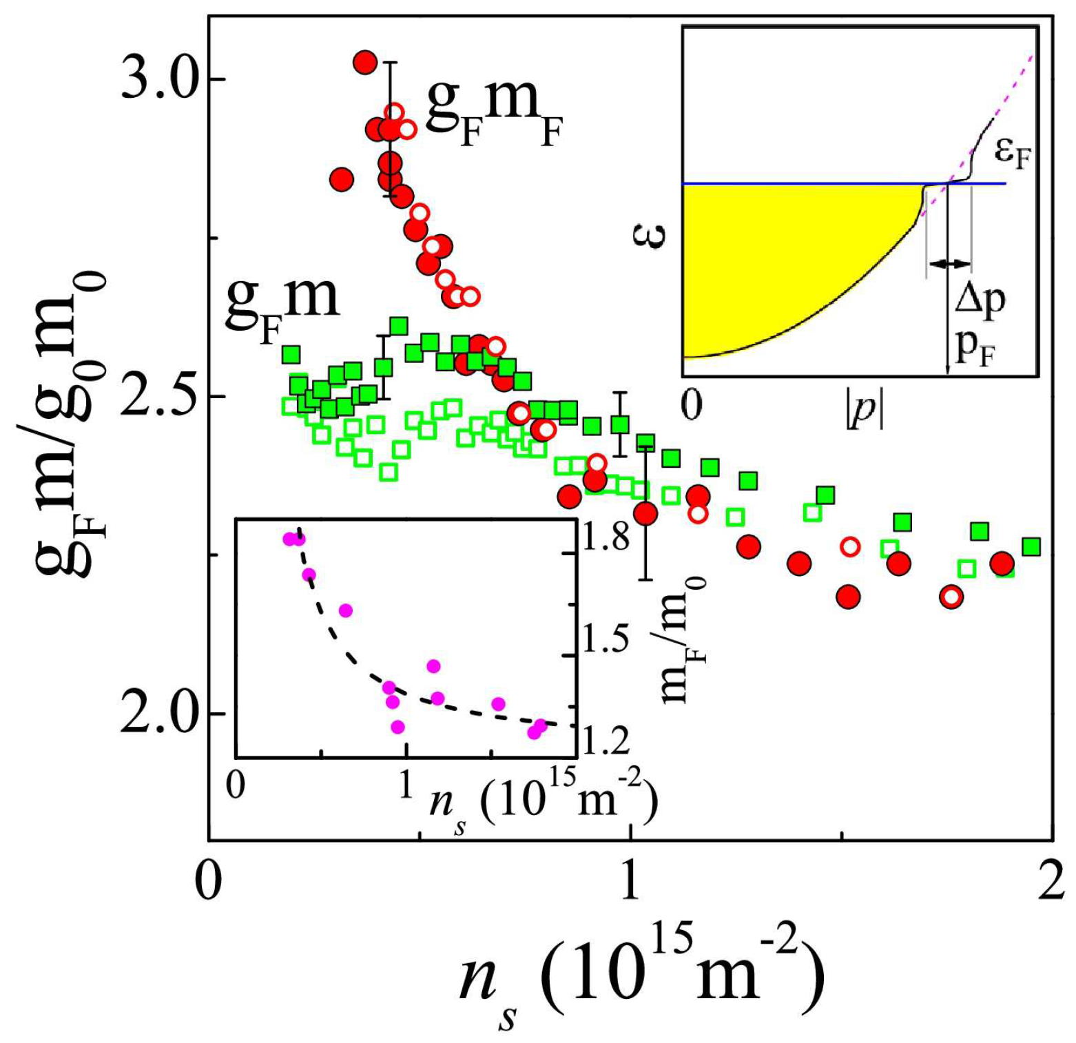
where is the Bohr magneton. Simultaneously, the authors studied Shubnikov–de Haas oscillations, yielding the product at the Fermi level. It turned out (see Figure 5) that with decreasing electron density (or increasing interaction strength), the product at the Fermi level monotonically increases in the entire range of electron densities, while the energy-averaged product saturates at low densities. Since the exchange effects in the 2D electron system in silicon are negligible, this difference can only be attributed to the different behaviors of the two effective masses. Their qualitatively different behavior reveals a precursor to the interaction-induced single-particle spectrum flattening at the Fermi level in this electron system.
It seems natural to interpret these experimental results within the concept of the fermion condensation [46,47,48]. The fermion condensation occurs at the Fermi level in a range of momenta, unlike the condensation of bosons. As the strength of electron–electron interactions increases, the single-particle spectrum flattens in a region near the Fermi momentum (top inset to Figure 5). At relatively high electron densities ( m), this effect is not important because the single-particle spectrum does not change noticeably in the interval , and the behaviors of the energy-averaged effective mass and that at the Fermi level are similar. However, decreasing the electron density in the range m stimulates the flattening of the spectrum so that the effective mass at the Fermi level, , continues to increase (here, is the Fermi velocity). In contrast, the energy-averaged effective mass does not, being not particularly sensitive to this flattening.
6. Transport Evidence for a Sliding Quantum Electron Solid
The insulating side of the metal-insulator transition has been extensively studied (see, e.g., [49,50,51,52,53]), but no definitive conclusion has been reached concerning the origin of the low-density state. The observed nonlinear current-voltage () curves were interpreted as either the manifestation of the depinning of an electron solid [50,51,52,54,55] or the breakdown of the insulating phase within traditional scenarios such as strong electric field Efros–Shklovskii variable range hopping [56] or percolation (see, e.g., Refs. [6,57] and the references therein). The observation of broad-band voltage noise at the threshold curves [50,51,52], as well as the attempts to probe the low-density state in perpendicular magnetic fields [53,58,59,60,61] also have not yielded information that allows a choice between the depinning of the electron solid or traditional mechanisms [6,57]. Much confusion was introduced by the fact that many authors chose to interpret their data in terms of the Wigner crystal [62,63,64,65,66], ignoring mundane interpretations.
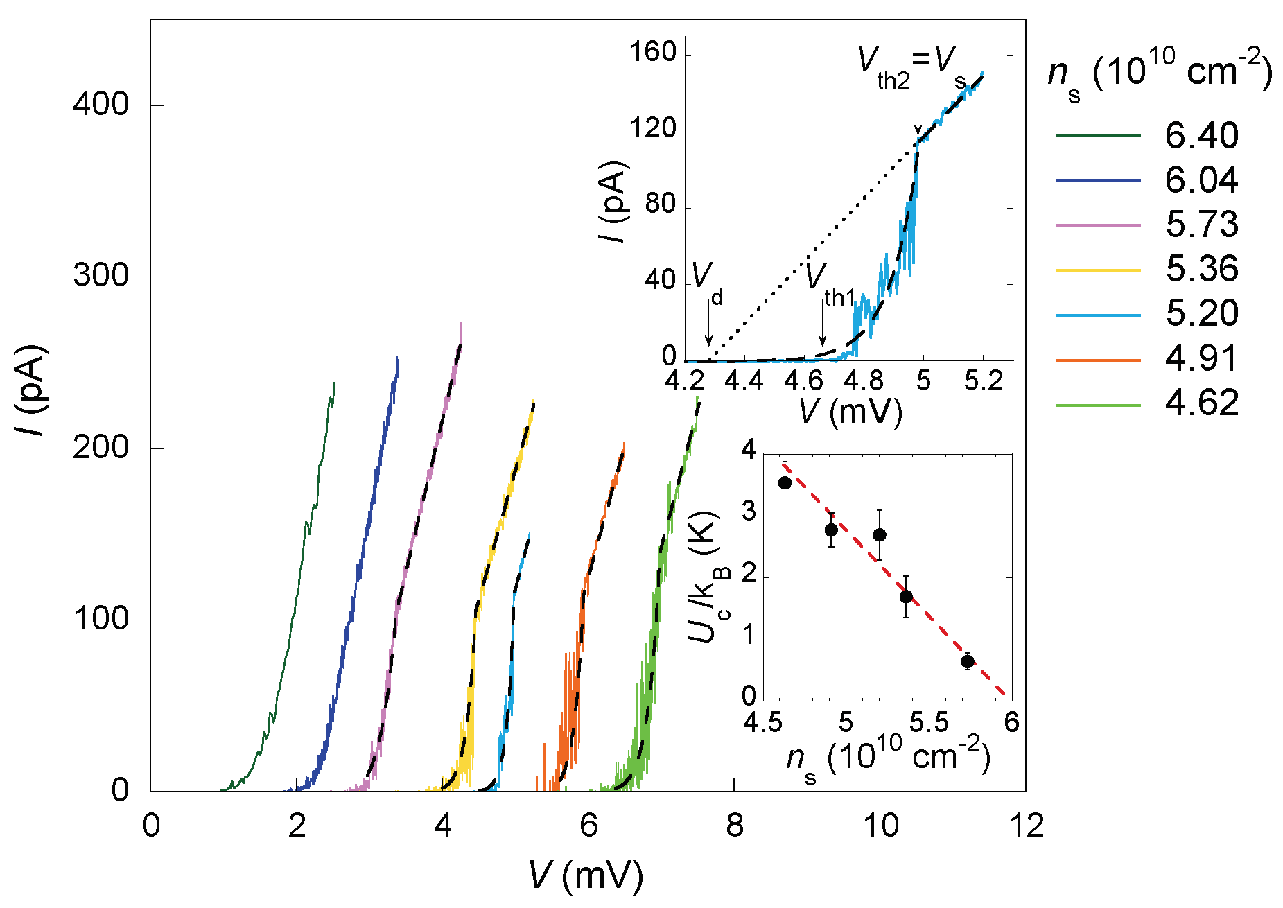
In [67], a significant breakthrough in the understanding of the origin of the low-density state has been reported. The authors observed two-threshold characteristics with a dramatic increase in noise between the two threshold voltages at the breakdown of the insulating state. The noise in current, in the form of fluctuations with time, dramatically increases above the first threshold, , and essentially disappears above the second threshold, . The double threshold behavior is very similar to that known for the collective depinning of the vortex lattice in Type-II superconductors (see, e.g., [68]) (provided the voltage and current axes are interchanged). This strongly favors the sliding 2D quantum electron solid, whereas the double threshold behavior cannot be described within alternative scenarios (percolation or overheating). Rather than being an ideal Wigner crystal, however, the 2D electron system described here is likely to be closer to an amorphous solid, which is similar to the case of the vortex lattice in Type-II superconductors where the collective pinning was observed.
In Figure 6, several low-temperature voltage-current curves at different electron densities in the insulating regime are shown. The corresponding interaction parameter exceeds . Two threshold voltages are observed at electron densities below cm: with increasing applied voltage, the current stays near zero up to a first voltage threshold , then increases sharply until a second threshold voltage is reached, above which the slope of the curve is significantly reduced and the curve is linear although not ohmic (see also the top inset to Figure 6). As the electron density is increased, the value of decreases, while the second threshold becomes less pronounced and eventually disappears. The authors observed no hysteresis in the range of electron densities studied. They pointed out that the observed behavior is quite distinct from the behavior reported in the insulating state in amorphous InO films, where the current was found to jump at the threshold voltage by as much as several orders of magnitude and the curves exhibited hysteresis consistent with bistability and electron overheating [69,70]. It is also worth noting that the occurrence of the double threshold cannot be explained within the percolation picture, in which case, a single threshold is expected [6]. Thus, the double threshold behavior cannot be described within existing traditional models.
Two remarks are due here. First, at electron density cm, below which the double-threshold behavior is evident, the interaction parameter is equal to ≈22. This is below the critical value at which the quantum Wigner crystallization in a disorder-free 2D system is expected to happen in zero magnetic field, according to the numerical simulations [64]. However, in subsequent simulations, it was shown that the crystallization should occur at lower values of when disorder is present [71]. Second, the disorder-independent divergence of the effective mass and the disorder-dependent formation of the quantum electron solid immediately imply the existence of an intermediate phase preceding the electron solidification. Indeed, the existence of such a phase was predicted in [46,65,72].
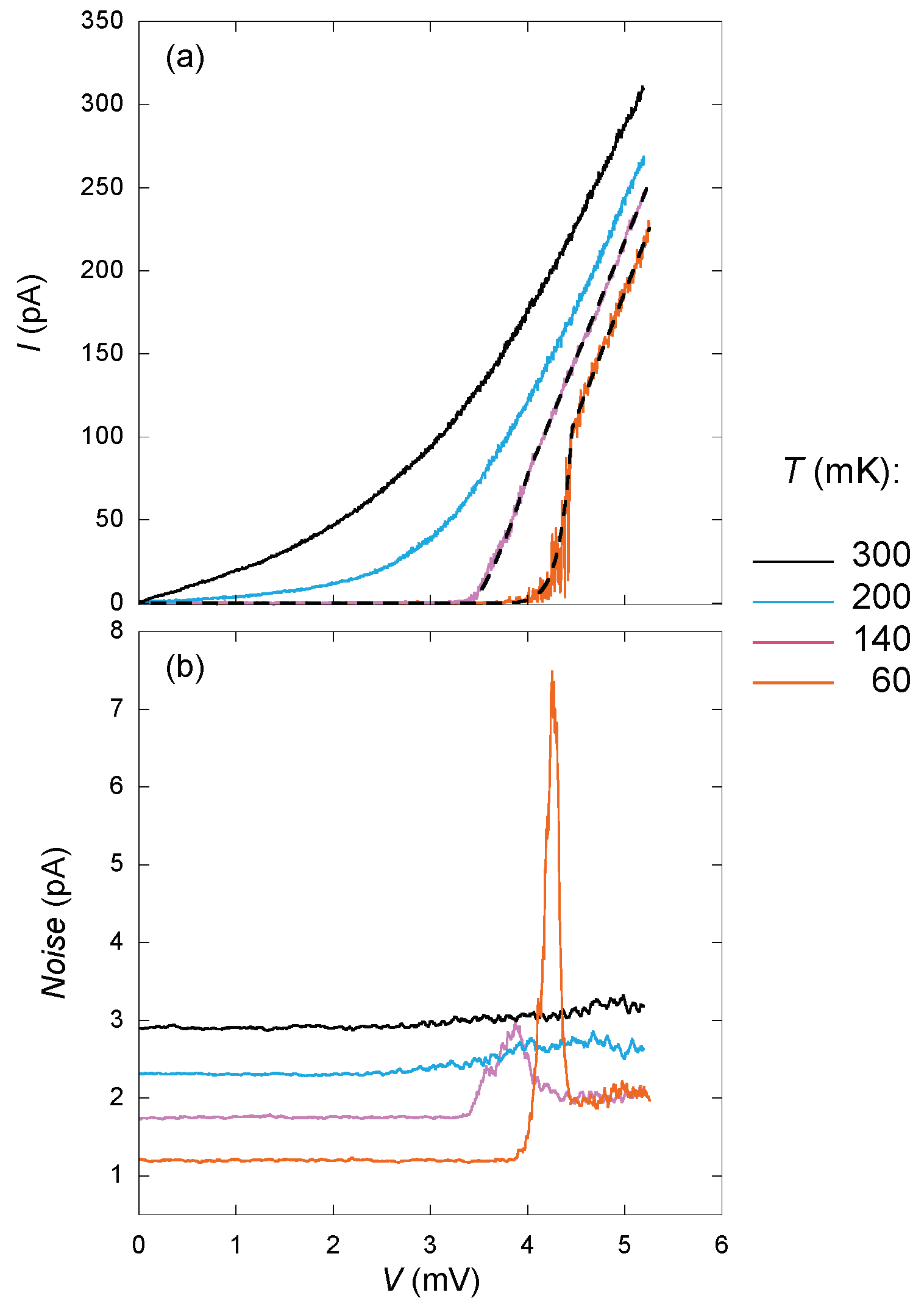
Figure 7a shows the characteristics for cm at different temperatures. As the temperature, T, is increased, the second threshold becomes less pronounced, and the threshold behavior of the curves eventually smears out due to the shrinkage of the zero-current interval. The measured broad-band noise is shown as a function of voltage in Figure 7b for different temperatures at electron density cm. A large increase in the noise is observed between the thresholds and at the lowest temperature. This large noise decreases rapidly with increasing temperature in agreement with the two-threshold behavior of the curves of Figure 7a. The frequency dependence of the noise amplitude is the law with , which is close to unity.
The authors of [67] analyzed their results in light of a phenomenological theory based on pinned elastic structures. Indeed, there is a striking similarity between the double-threshold dependences in the low- state of Si MOSFETs and those (with the voltage and current axes interchanged) known for the collective depinning of the vortex lattice in Type-II superconductors (see, e.g., [68]). The physics of the vortex lattice in the latter system, in which the existence of two thresholds is well documented, can be adapted for the case of an electron solid. In a superconductor, current flows for zero voltage; the depinning of the vortex lattice occurs when a non-zero voltage appears. In the authors’ case, the situation is reciprocal: a finite voltage is applied, but at first, the current is not flowing in the limit of zero temperature; the depinning of the electron solid is indicated by the appearance of a non-zero current. The intermediate regime between the dynamic () and static () thresholds corresponds to the collective pinning of the solid. In this region, the pinning occurs at the centers with different energies, and the current is thermally activated:
where is the activation energy. The static threshold signals the onset of the regime of solid motion with friction. This corresponds to the condition:
(here, E is the electric field and L is the characteristic distance between the pinning centers with maximal activation energy ). The balance of the electric, pinning, and friction forces in the regime of solid motion with friction yields a linear characteristic that is offset by the threshold corresponding to the pinning force:
where is a coefficient (near , one can in general expect a power-law behavior of ). Assuming that the activation energy for the electron solid is equal to:
the authors obtained the expression for the current:
The fits to the data using Equation (6) are shown by dashed lines in Figure 6 and Figure 7a. Equation (6) successfully describes the experimentally observed two-threshold characteristics. The value of decreases approximately linearly with electron density and reaches zero at cm (the bottom inset to Figure 6) (note that this is in contrast to the vanishing activation energy of electron-hole pairs at obtained by measurements of the resistance in the limit of zero voltages/currents [17]). Probably, the vanishing is related to the minimum number of the strong pinning centers for which the collective pinning is still possible. The coefficient is approximately constant ( Ohm), and this indicates that the solid motion with friction is controlled by weak pinning centers [68]. The authors of [67] argue that the large noise in the regime of the collective pinning of the solid between and should be suppressed in the regime of solid motion with friction at . Indeed, in the regime of the collective pinning of the solid between and , the solid deforms locally when the depinning occurs at some center, and then, this process repeats at another center, etc., which leads to the generation of a large noise. In contrast, in the regime of solid motion with friction above the second threshold , the solid slides as a whole due to the over-barrier motion, and, therefore, the noise is suppressed. Thus, the physics of pinned periodic/elastic objects is relevant for the low-density state in a 2D electron system in silicon MOSFETs. These experimental results are also consistent with numerical simulations of the dynamics of a 2D electron system forming a Wigner solid in the presence of charged impurities [73,74].
7. Summary
In summary, we have reviewed the exciting properties of strongly-interacting fermions in 2D electron and hole systems, in particular transport and thermodynamic data on the metallic side of the metal-insulator transition and recent advances in our understanding of the low-density state on the insulating side of the transition. A complementary review [61] of the low-density state is available in the same volume.
Funding
A.A.S. was supported by RFBR 18-02-00368 and 19-02-00196, RAS, and the Russian Government Contract. S.V.K. was supported by NSF Grant No. 1309337 and BSF Grant No. 2012210.
Acknowledgments
We are grateful to V.T. Dolgopolov for careful reading of the manuscript and illuminating discussions.
Conflicts of Interest
The authors declare no conflict of interest.
References
- Zavaritskaya, T.N.; Zavaritskaya, É.I. Metal-insulator transition in inversion channels of silicon MOS structures. JETP Lett. 1987, 45, 609–613. [Google Scholar]
- Kravchenko, S.V.; Kravchenko, G.V.; Furneaux, J.E.; Pudalov, V.M.; D’Iorio, M. Possible metal-insulator transition at B = 0 in two dimensions. Phys. Rev. B 1994, 50, 8039–8042. [Google Scholar] [CrossRef]
- Popović, D.; Fowler, A.B.; Washburn, S. Metal-insulator transition in two dimensions: Effects of disorder and magnetic field. Phys. Rev. Lett. 1997, 79, 1543–1546. [Google Scholar] [CrossRef]
- Abrahams, E.; Kravchenko, S.V.; Sarachik, M.P. Metallic behavior and related phenomena in two dimensions. Rev. Mod. Phys. 2001, 73, 251–266. [Google Scholar] [CrossRef]
- Kravchenko, S.V.; Sarachik, M.P. Metal-insulator transition in two-dimensional electron systems. Rep. Prog. Phys. 2004, 67, 1–44. [Google Scholar] [CrossRef]
- Shashkin, A.A. Metal-insulator transitions and the effects of electron-electron interactions in two-dimensional electron systems. Phys. Usp. 2005, 48, 129–149. [Google Scholar] [CrossRef]
- Spivak, B.; Kravchenko, S.V.; Kivelson, S.A.; Gao, X.P.A. Transport in strongly correlated two dimensional electron fluids. Rev. Mod. Phys. 2010, 82, 1743–1766. [Google Scholar] [CrossRef]
- Melnikov, M.Y.; Shashkin, A.A.; Dolgopolov, V.T.; Zhu, A.Y.X.; Kravchenko, S.V.; Huang, S.-H.; Liu, C.W. Quantum phase transition in ultrahigh mobility SiGe/Si/SiGe two-dimensional electron system. Phys. Rev. B 2019, 99, 081106(R). [Google Scholar] [CrossRef]
- Punnoose, A.; Finkelstein, A.M. Dilute electron gas near the metal-insulator transition: Role of valleys in silicon inversion layers. Phys. Rev. Lett. 2001, 88, 016802. [Google Scholar] [CrossRef]
- Punnoose, A.; Finkelstein, A.M. Metal-insulator transition in disordered two-dimensional electron systems. Science 2005, 310, 289–291. [Google Scholar] [CrossRef]
- Finkelstein, A.M. Influence of Coulomb interaction on the properties of disordered metals. Sov. Phys. JETP 1983, 57, 97–108. [Google Scholar]
- Finkelstein, A.M. Weak localization and Coulomb interaction in disordered systems. Z. Phys. B 1984, 56, 189–196. [Google Scholar] [CrossRef]
- Castellani, C.; Di Castro, C.; Lee, P.A.; Ma, M. Interaction-driven metal-insulator transitions in disordered fermion systems. Phys. Rev. B 1984, 30, 527–543. [Google Scholar] [CrossRef]
- Castellani, C.; Di Castro, C.; Lee, P.A. Metallic phase and metal-insulator transition in two-dimensional electronic systems. Phys. Rev. B 1998, 57, R9381–R9384. [Google Scholar] [CrossRef]
- Kravchenko, S.V.; Mason, W.E.; Bowker, G.E.; Furneaux, J.E.; Pudalov, V.M.; D’Iorio, M. Scaling of an anomalous metal-insulator transition in a two-dimensional system in silicon at B = 0. Phys. Rev. B 1995, 51, 7038–7045. [Google Scholar] [CrossRef]
- Hanein, Y.; Meirav, U.; Shahar, D.; Li, C.C.; Tsui, D.C.; Shtrikman, H. The metalliclike conductivity of a two-dimensional hole system. Phys. Rev. Lett. 1998, 80, 1288–1291. [Google Scholar] [CrossRef]
- Shashkin, A.A.; Kravchenko, S.V.; Klapwijk, T.M. Metal-insulator transition in a 2D electron gas: Equivalence of two approaches for determining the critical point. Phys. Rev. Lett. 2001, 87, 266402. [Google Scholar] [CrossRef] [PubMed]
- Kravchenko, S.V.; Klapwijk, T.M. Metallic low-temperature resistivity in a 2D electron system over an extended temperature range. Phys. Rev. Lett. 2000, 84, 2909–2912. [Google Scholar] [CrossRef]
- Simonian, D.; Kravchenko, S.V.; Sarachik, M.P.; Pudalov, V.M. Magnetic field suppression of the conducting phase in two dimensions. Phys. Rev. Lett. 1997, 79, 2304–2307. [Google Scholar] [CrossRef]
- Pudalov, V.M.; Brunthaler, G.; Prinz, A.; Bauer, G. Instability of the two-dimensional metallic phase to a parallel magnetic field. JETP Lett. 1997, 65, 932–937. [Google Scholar] [CrossRef]
- Gao, X.P.A.; Boebinger, G.S.; Mills, A.P., Jr.; Ramirez, A.P.; Pfeiffer, L.N.; West, K.W. Spin-polarization-induced tenfold magnetoresistivity of highly metallic two-dimensional holes in a narrow GaAs quantum well. Phys. Rev. B 2006, 73, 241315(R). [Google Scholar] [CrossRef]
- Dolgopolov, V.T.; Gold, A. Magnetoresistance of a two-dimensional electron gas in a parallel magnetic field. JETP Lett. 2000, 71, 27–30. [Google Scholar] [CrossRef]
- Okamoto, T.; Hosoya, K.; Kawaji, S.; Yagi, A. Spin degree of freedom in a two-dimensional electron liquid. Phys. Rev. Lett. 1999, 82, 3875–3878. [Google Scholar] [CrossRef]
- Vitkalov, S.A.; Zheng, H.; Mertes, K.M.; Sarachik, M.P.; Klapwijk, T.M. Small-angle Shubnikov-de Haas measurements in a 2D electron system: The effect of a strong in-plane magnetic field. Phys. Rev. Lett. 2000, 85, 2164–2167. [Google Scholar] [CrossRef] [PubMed]
- Dolgopolov, V.T.; Kravchenko, G.V.; Shashkin, A.A.; Kravchenko, S.V. Properties of electron insulating phase in Si inversion layers at low-temperatures. JETP Lett. 1992, 55, 733–737. [Google Scholar]
- Dolgopolov, V.T.; Shashkin, A.A.; Kravchenko, S.V. Spin polarization and exchange-correlation effects in transport properties of two-dimensional electron systems in silicon. Phys. Rev. B 2017, 96, 075307. [Google Scholar] [CrossRef]
- Li, S.; Sarachik, M.P. Resistivity of the insulating phase approaching the two-dimensional metal-insulator transition: The effect of spin polarization. Phys. Rev. B 2017, 95, 041301(R). [Google Scholar] [CrossRef]
- Kravchenko, S.V.; Shashkin, A.A.; Bloore, D.A.; Klapwijk, T.M. Shubnikov-de Haas oscillations near the metal-insulator transition in a two-dimensional electron system in silicon. Solid State Commun. 2000, 116, 495–499. [Google Scholar] [CrossRef]
- Shashkin, A.A.; Kravchenko, S.V.; Dolgopolov, V.T.; Klapwijk, T.M. Indication of the ferromagnetic instability in a dilute two-dimensional electron system. Phys. Rev. Lett. 2001, 87, 086801. [Google Scholar] [CrossRef]
- Shashkin, A.A.; Anissimova, S.; Sakr, M.R.; Kravchenko, S.V.; Dolgopolov, V.T.; Klapwijk, T.M. Pauli spin susceptibility of a strongly correlated two-dimensional electron liquid. Phys. Rev. Lett. 2006, 96, 036403. [Google Scholar] [CrossRef]
- Kozuka, Y.; Tsukazaki, A.; Kawasaki, M. Challenges and opportunities of ZnO-related single crystalline heterostructures. Appl. Phys. Rev. 2014, 1, 011303. [Google Scholar] [CrossRef]
- Shashkin, A.A.; Kravchenko, S.V.; Dolgopolov, V.T.; Klapwijk, T.M. Sharp increase of the effective mass near the critical density in a metallic two-dimensional electron system. Phys. Rev. B 2002, 66, 073303. [Google Scholar] [CrossRef]
- Shashkin, A.A.; Rahimi, M.; Anissimova, S.; Kravchenko, S.V.; Dolgopolov, V.T.; Klapwijk, T.M. Spin-independent origin of the strongly enhanced effective mass in a dilute 2D electron system. Phys. Rev. Lett. 2003, 91, 046403. [Google Scholar] [CrossRef] [PubMed]
- Anissimova, S.; Venkatesan, A.; Shashkin, A.A.; Sakr, M.R.; Kravchenko, S.V.; Klapwijk, T.M. Magnetization of a strongly interacting two-dimensional electron system in perpendicular magnetic fields. Phys. Rev. Lett. 2006, 96, 046409. [Google Scholar] [CrossRef] [PubMed]
- Mokashi, A.; Li, S.; Wen, B.; Kravchenko, S.V.; Shashkin, A.A.; Dolgopolov, V.T.; Sarachik, M.P. Critical behavior of a strongly interacting 2D electron system. Phys. Rev. Lett. 2012, 109, 096405. [Google Scholar] [CrossRef]
- Heikkila, T.T.; Kopnin, N.B.; Volovik, G.E. Flat bands in topological media. JETP Lett. 2011, 94, 233–239. [Google Scholar] [CrossRef]
- Bennemann, K.-H.; Ketterson, J.B. Novel Superfluids; Oxford University Press: Oxford, UK, 2013. [Google Scholar]
- Peotta, S.; Torma, P. Superfluidity in topologically nontrivial flat bands. Nat. Commun. 2015, 6, 8944. [Google Scholar] [CrossRef]
- Volovik, G.E. From standard model of particle physics to room-temperature superconductivity. Phys. Scr. 2015, T164, 014014. [Google Scholar] [CrossRef]
- Amusia, M.Y.; Popov, K.G.; Shaginyan, V.R.; Stephanovich, V.A. Theory of Heavy Fermion Compounds; Springer: Berlin, Germany, 2014. [Google Scholar]
- Camjayi, A.; Haule, K.; Dobrosavljević, V.; Kotliar, G. Coulomb correlations and the Wigner-Mott transition. Nat. Phys. 2008, 4, 932–935. [Google Scholar] [CrossRef]
- Yudin, D.; Hirschmeier, D.; Hafermann, H.; Eriksson, O.; Lichtenstein, A.I.; Katsnelson, M.I. Fermi condensation near van Hove singularities within the Hubbard model on the triangular lattice. Phys. Rev. Lett. 2014, 112, 070403. [Google Scholar] [CrossRef] [PubMed]
- Melnikov, M.Y.; Shashkin, A.A.; Dolgopolov, V.T.; Huan, S.-H.; Liu, C.W.; Kravchenko, S.V. Indication of band flattening at the Fermi level in a strongly correlated electron system. Sci. Rep. 2017, 7, 14539. [Google Scholar] [CrossRef] [PubMed]
- Melnikov, M.Y.; Shashkin, A.A.; Dolgopolov, V.T.; Huan, S.-H.; Liu, C.W.; Kravchenko, S.V. Ultra-high mobility two-dimensional electron gas in a SiGe/Si/SiGe quantum well. Appl. Phys. Lett. 2015, 106, 092102. [Google Scholar] [CrossRef]
- Melnikov, M.Y.; Shashkin, A.A.; Dolgopolov, V.T.; Kravchenko, S.V.; Huan, S.-H.; Liu, C.W. Effective electron mass in high-mobility SiGe/Si/SiGe quantum wells. JETP Lett. 2014, 100, 114–119. [Google Scholar] [CrossRef]
- Khodel, V.A.; Shaginyan, V.R. Superfluidity in system with fermion condensate. JETP Lett. 1990, 51, 553–555. [Google Scholar]
- Nozières, P. Properties of Fermi liquids with a finite range interaction. J. Phys. I 1992, 2, 443–458. [Google Scholar] [CrossRef]
- Zverev, M.V.; Khodel, V.A.; Pankratov, S.S. Microscopic theory of a strongly correlated two-dimensional electron gas. JETP Lett. 2012, 96, 192–202. [Google Scholar] [CrossRef]
- Andrei, E.Y.; Deville, G.; Glattli, D.C.; Williams, F.I.B.; Paris, E.; Etienne, B. Observation of a magnetically induced Wigner solid. Phys. Rev. Lett. 1988, 60, 2765–2768. [Google Scholar] [CrossRef]
- Goldman, V.J.; Santos, M.; Shayegan, M.; Cunningham, J.E. Evidence for two-dimensional quantum Wigner crystal. Phys. Rev. Lett. 1990, 65, 2189–2192. [Google Scholar] [CrossRef] [PubMed]
- Kravchenko, S.V.; Pudalov, V.M.; Campbell, J.; D’Iorio, M. Electron solid at the Si surface in zero magnetic field? JETP Lett. 1991, 54, 532–536. [Google Scholar]
- Pudalov, V.M.; D’Iorio, M.; Kravchenko, S.V.; Campbell, J.W. Zero-magnetic-field collective insulator phase in a dilute 2D electron system. Phys. Rev. Lett. 1993, 70, 1866–1869. [Google Scholar] [CrossRef] [PubMed]
- Knighton, T.; Wu, Z.; Huang, J.; Serafin, A.; Xia, J.S.; Pfeiffer, L.N.; West, K.W. Evidence of two-stage melting of Wigner solids. Phys. Rev. B 2018, 97, 085135. [Google Scholar] [CrossRef]
- Williams, F.I.B.; Wright, P.A.; Clark, R.G.; Andrei, E.Y.; Deville, G.; Glattli, D.C.; Probst, O.; Etienne, B.; Dorin, C.; Foxon, C.T.; et al. Conduction threshold and pinning frequency of magnetically induced Wigner solid. Phys. Rev. Lett. 1991, 66, 3285–3288. [Google Scholar] [CrossRef] [PubMed]
- Chitra, R.; Giamarchi, T. Zero field Wigner crystal. Eur. Phys. J. B 2005, 44, 455–467. [Google Scholar] [CrossRef]
- Marianer, S.; Shklovskii, B.I. Effective temperature of hopping electrons in a strong electric field. Phys. Rev. B 1992, 46, 13100–13103. [Google Scholar] [CrossRef]
- Jiang, H.W.; Stormer, H.L.; Tsui, D.C.; Pfeiffer, L.N.; West, K.W. Magnetotransport studies of the insulating phase around ν=1/5 Landau-level filling. Phys. Rev. B 1991, 44, 8107–8114. [Google Scholar] [CrossRef]
- D’Iorio, M.; Pudalov, V.M.; Semenchinsky, S.G. Magnetic field induced transitions between quantized Hall and insulator states in a dilute 2D electron gas. Phys. Lett. A 1990, 150, 422–426. [Google Scholar] [CrossRef]
- D’Iorio, M.; Pudalov, V.M.; Semenchinsky, S.G. Reentrant insulating phase in Si inversion layers in low magnetic fields. Phys. Rev. B 1992, 46, 15992–16004. [Google Scholar] [CrossRef]
- Qiu, R.L.J.; Gao, X.P.A.; Pfeiffer, L.N.; West, K.W. Connecting the reentrant insulating phase and the zero-field metal-insulator transition in a 2D hole system. Phys. Rev. Lett. 2012, 108, 106404. [Google Scholar] [CrossRef] [PubMed]
- Qiu, R.L.J.; Liu, C.W.; Liu, S.; Gao, X.P.A. New reentrant insulating phases in strongly interacting 2D systems with low disorder. Appl. Sci. 2018, 8, 1909. [Google Scholar] [CrossRef]
- Wigner, E. On the interaction of electrons in metals. Phys. Rev. 1934, 46, 1002–1011. [Google Scholar] [CrossRef]
- Chaplik, A.V. Possible crystallization of charge carriers in low-density inversion layers. Sov. Phys. JETP 1972, 35, 395–398. [Google Scholar]
- Tanatar, B.; Ceperley, D.M. Ground state of the two-dimensional electron gas. Phys. Rev. B 1989, 39, 5005–5016. [Google Scholar] [CrossRef]
- Attaccalite, C.; Moroni, S.; Gori-Giorgi, P.; Bachelet, G.B. Correlation energy and spin polarization in the 2D electron gas. Phys. Rev. Lett. 2002, 88, 256601. [Google Scholar] [CrossRef]
- Dolgopolov, V.T. Quantum melting of a two-dimensional Wigner crystal. Phys. Usp. 2017, 60, 731–742. [Google Scholar] [CrossRef]
- Brussarski, P.; Li, S.; Kravchenko, S.V.; Shashkin, A.A.; Sarachik, M.P. Transport evidence for a sliding two-dimensional quantum electron solid. Nat. Commun. 2018, 9, 3803. [Google Scholar] [CrossRef]
- Blatter, G.; Feigel’man, M.Y.; Geshkenbein, Y.B.; Larkin, A.I.; Vinokur, V.M. Vortices in high-temperature superconductors. Rev. Mod. Phys. 1994, 66, 1125–1388. [Google Scholar] [CrossRef]
- Ovadia, M.; Sacepe, B.; Shahar, D. Electron-phonon decoupling in disordered insulators. Phys. Rev. Lett. 2009, 102, 176802. [Google Scholar] [CrossRef] [PubMed]
- Altshuler, B.L.; Kravtsov, V.E.; Lerner, I.V.; Aleiner, I.L. Jumps in current-voltage characteristics in disordered films. Phys. Rev. Lett. 2009, 102, 176803. [Google Scholar] [CrossRef]
- Chui, S.T.; Tanatar, B. Impurity effect on the two-dimensional-electron fluid-solid transition in zero field. Phys. Rev. Lett. 1995, 74, 458–461. [Google Scholar] [CrossRef] [PubMed]
- Spivak, B.; Kivelson, S.A. Phases intermediate between a two-dimensional electron liquid and Wigner crystal. Phys. Rev. B 2004, 70, 155114. [Google Scholar] [CrossRef]
- Reichhardt, C.; Olson, C.J.; Grønbech-Jensen, N.; Nori, F. Moving Wigner glasses and smectics: Dynamics of disordered Wigner crystals. Phys. Rev. Lett. 2001, 86, 4354–4357. [Google Scholar] [CrossRef]
- Reichhardt, C.; Olson Reichhardt, C.J. Depinning and nonequilibrium dynamic phases of particle assemblies driven over random and ordered substrates: A review. Rep. Prog. Phys. 2017, 80, 026501. [Google Scholar] [CrossRef]
Figure 1.
Resistivity as a function of temperature in a Si MOSFET (a), p-type GaAs/AlGaAs heterostructure (b), and SiGe/Si/SiGe quantum well (c). Figures adapted from [15], [16], and [8], respectively.

Figure 2.
(a) Resistivity vs. parallel magnetic field measured at K in a Si MOSFET. Densities are indicated in units of cm; from [20]. (b) Resistivity as a function of in a 10 nm-wide p-type GaAs quantum well at 20 mK; from [21].

Figure 3.
Temperature dependence of the resistivity of a Si MOSFET at different electron densities near the MIT in zero magnetic field (a) and in a parallel magnetic field of 4 Tesla (b). The electron densities are indicated in units of cm. Dashed curves correspond to , which is equal to cm in zero field and to cm in Tesla. Adapted from [17].

Figure 4.
(a) Dependence of the Pauli spin susceptibility on electron density in a silicon MOSFET obtained by three independent methods: thermodynamic measurements of the magnetization (dashed line), the magnetic field of the full spin polarization (circles), and magnetocapacitance (squares). The dotted line is a guide to the eye. Also shown by a solid line are the transport data of [29]. The inset shows the polarization field as a function of the electron density determined from the magnetization (circles) and magnetocapacitance (squares) data. The symbol size for the magnetization data reflects the experimental uncertainty. The dependence extrapolates linearly to zero field at a density just below . Adapted from [30]. (b) The effective electron mass m (circles) and g-factor (squares) in a silicon MOSFET, determined from the analysis of the parallel field magnetoresistance and temperature-dependent conductivity, versus electron density. and are the electron mass and g-factor for non-interacting electrons in silicon. The dashed lines are guides to the eye. Adapted from [32].

Figure 5.
Product of the Landé factor and effective mass as a function of electron density in a SiGe/Si/SiGe quantum well determined by measurements of the field of full spin polarization (squares) and Shubnikov–de Haas oscillations (circles) at mK. The empty and filled symbols correspond to two samples. The experimental uncertainty corresponds to the data dispersion and is about 2% for the squares and about 4% for the circles ( and are the values for non-interacting electrons; is the free electron mass; and is the g-factor at the Fermi level). The top inset shows schematically the single-particle spectrum of the electron system in a state preceding the band flattening at the Fermi level (solid black line). The dashed violet line corresponds to an ordinary parabolic spectrum. The occupied electron states at are indicated by the shaded area. Bottom inset: the effective mass versus electron density determined by analysis of the temperature dependence of the amplitude of Shubnikov–de Haas oscillations, similar to [45]. The dashed line is a guide to the eye. From [43].

Figure 6.
curves are shown for different electron densities in the insulating state of a silicon MOSFET at a temperature of 60 mK. The dashed lines are fits to the data using Equation (6). The top inset shows the curve for cm on an expanded scale; also shown are the threshold voltages and , the static threshold , and the dynamic threshold that is obtained by the extrapolation of the linear region of the curve to zero current. Bottom inset: activation energy vs. electron density. Vertical error bars represent standard deviations in the determination of from the fits to the data using Equation (6). The dashed line is a linear fit. From [67].

Figure 7.
(a) characteristics at cm in a silicon MOSFET for different temperatures. The dashed lines are fits to the data using Equation (6). (b) The broad-band noise as a function of voltage for the same electron density and temperatures. The three upper curves are shifted vertically for clarity. From [67].

© 2019 by the authors. Licensee MDPI, Basel, Switzerland. This article is an open access article distributed under the terms and conditions of the Creative Commons Attribution (CC BY) license (http://creativecommons.org/licenses/by/4.0/).
Share and Cite
MDPI and ACS Style
Shashkin, A.A.; Kravchenko, S.V. Recent Developments in the Field of the Metal-Insulator Transition in Two Dimensions. Appl. Sci. 2019, 9, 1169. https://doi.org/10.3390/app9061169
AMA Style
Shashkin AA, Kravchenko SV. Recent Developments in the Field of the Metal-Insulator Transition in Two Dimensions. Applied Sciences. 2019; 9(6):1169. https://doi.org/10.3390/app9061169
Chicago/Turabian StyleShashkin, Alexander A., and Sergey V. Kravchenko. 2019. "Recent Developments in the Field of the Metal-Insulator Transition in Two Dimensions" Applied Sciences 9, no. 6: 1169. https://doi.org/10.3390/app9061169
Note that from the first issue of 2016, this journal uses article numbers instead of page numbers. See further details here.