Comparative Study of Nano-Slot Silicon Waveguides Covered by Dye Doped and Undoped Polymer Cladding


1
Research Group for Photonics, Laser and Plasmatechnologies, Technical University of Applied Sciences Wildau, Hochschulring 1, 15745 Wildau, Germany
2
IHP—Leibniz-Institut für Innovative Mikroelektronik, Im Technologiepark 25, 15236 Frankfurt (Oder), Germany
*
Author to whom correspondence should be addressed.
Appl. Sci. 2019, 9(1), 89; https://doi.org/10.3390/app9010089
Submission received: 17 November 2018
/
Revised: 11 December 2018
/
Accepted: 20 December 2018
/
Published: 27 December 2018
(This article belongs to the Special Issue Frontiers in Nanophotonics 2019)
Abstract
:Nonlinear optical dyes doped in optical polymer matrices are widely used for electro-optical devices. Linear optical properties change with dye concentration, which leads to a change in modal properties, especially in nano-structured integrated waveguides such as silicon slot-waveguides. Here, we investigate the influence of a nonlinear optical dye on the performance of a silicon-organic hybrid slot-waveguide. A simulation study of the modal and optical confinement properties is carried out and dependence of the structural parameters of the slot-waveguide and the organic cladding material is taken into account. As cladding material, a guest-host polymer system is employed comprising the nonlinear optical dye Disperse Red 1 (DR1) doped in a poly[methyl methacrylate] (PMMA) matrix. The refractive indices of doped and undoped PMMA were deduced from ellipsometric data. We present a guideline for an optimized slot-waveguide design for the fabrication in silicon-on-insulator technology giving rise to scalable, high-performance integrated electro-optical modulators.
1. Introduction
Silicon-organic hybrid (SOH) photonics has gained a lot of attention in recent years due to its potential for high-speed modulators [1,2]. Electro-optical (EO) polymers incorporated into silicon-on-insulator (SOI) slot-waveguides with gap sizes below have lead to unrivaled results in high-speed performance. There are two EO effects present in EO polymers; namely the linear [3] and the quadratic EO effect [4]. The former one has been widely investigated in SOH modulators. Recently, SOH Mach-Zehnder modulators with exceptionally low energy consumption of have been demonstrated using the linear EO effect having record-high in-device EO figures of merit of up to [5]. Furthermore, data rates of up to in on-off keying (OOK) operation and voltage-length products as low as have been reported [6].
The performance of those devices is achieved by the introduction of SOI slot-waveguides with polymer-clad. Within a narrow, low-index gap region, slot-waveguides offer a high optical field confinement [7], which can be exploited to efficiently modulate the guided mode. The large optical and electrical field overlap in SOI slot-waveguides allows for ultra-efficient EO modulation. The EO response is provided by the polymer-clad. A widely used polymer system consists of the linear conjugated dye Disperse Red 1 (DR1) doped into a poly[methyl methacrylate] (PMMA) matrix [8]. It was used to demonstrate the feasibility of employing the linear [9] as well as the quadaratic EO effect in SOI slot-waveguides demonstrating its high potential for SOH photonics [4]. The polymer system PMMA+DR1 is commercially available (Sigma Aldrich, St. Louis, MO, USA) and can be used as a test material since it is cost effective and the sample preparation is relatively simple. However, the optical properties of the polymer is changed by the EO dye DR1. Therefore, it is desirable to study the influence of this change on the modal-field distribution in slot-waveguides. For high scalability and reduction of costs this approach requires compatibility to complementary metal-oxide semiconductor (CMOS)-technologies.
In this work, we consider CMOS-compatible slot-waveguides based on SOI substrates covered with a polymer-clad consisting of the guest-host polymer system PMMA+DR1. For the first time, our investigation focuses on the influence of the nonlinear optical dye concentration on the modal properties of slot-waveguides and compares it with the influence of geometric parameters. The precise knowledge of the effective refractive index is crucial for the design of waveguide couplers and for highly efficient phase-matched second harmonic generation [10,11]. Beside that, the field confinement factor is from great importance for the optimization of EO modulators. Therefore, we provide precise values for the effective refractive index and a guideline to optimize the field confinement factor.
2. Theoretical Background
2.1. Organic Polymers in Silicon Photonics
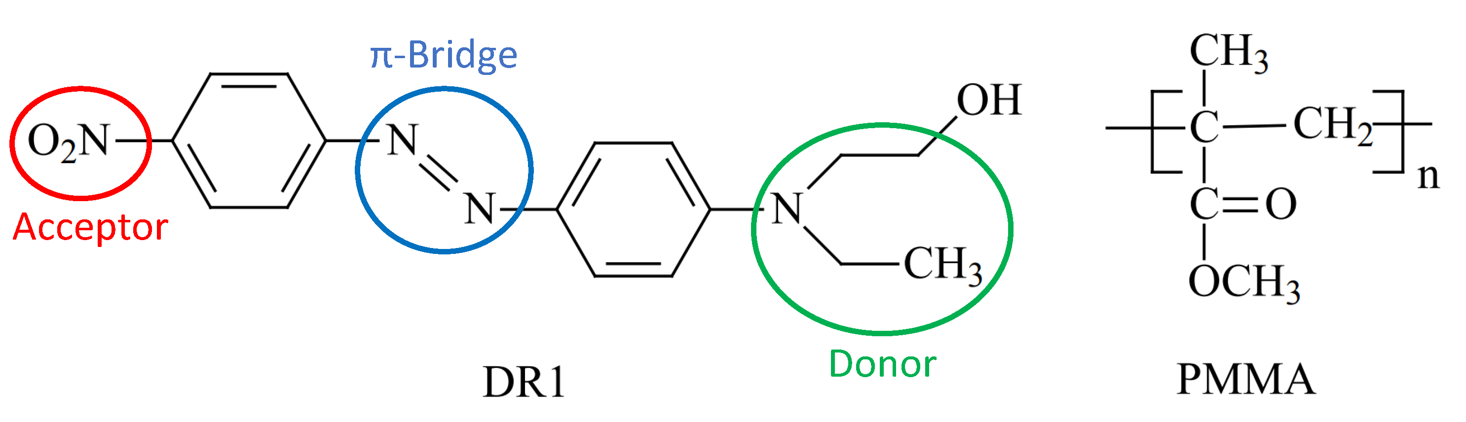
A guest-host polymer system consisting of the azo benzene dye Disperse Red 1 (DR1) in a poly[methyl methacrylate] (PMMA) matrix is employed as the electro-optical medium in this work and is called PMMA+DR1 in the following. The chemical structure of both components is presented in Figure 1. DR1 is a non-centro-symmetric organic chromophore, where the donor and acceptor molecules are bonded through a conjugated -bridge. acts as an acceptor, while the conjugated -bridge allows the transport of charges, which are donated by the alkyl-amino-group. The weakly bound -electrons in this system already offer a charge displacement which leads to a high polarizability through applied electrical fields. Large dipole moments and therefor a high nonlinear optical efficiency are clear advantages of this medium, considering a photonic modulation purpose [12,13]. Additionally, the usage of EO polymers shows low free-carrier dispersion, which usually is the fundamental speed limitation in silicon photonics modulators [14]. Moreover, an intrinsic coupling of amplitude and phase of the EO material can be achieved, making advanced modulation formats such as 16-state quadrature amplitude modulation (16QAM) or quadrature phase-shift keying (QPSK) possible [3,15].
Figure 2 shows the dispersion curves for PMMA+DR1, measured by ellipsometry. The values are given for two different mass concentrations (weight percentages) C in wt% of the DR1 chromophore within the polymer matrix PMMA. The extinction coefficient is zero over the entire wavelength range for , while it has an absorption peak of at for . However, for applications in silicon photonics, the to range (red-striped box) is from great importance, due to the transmission window of silicon [16]. At the optical telecommunication C-band wavelength , the measured refractive indices are and , respectively, showing a normal dispersion behavior.
2.2. Silicon-on-Insulator Slot-Waveguides
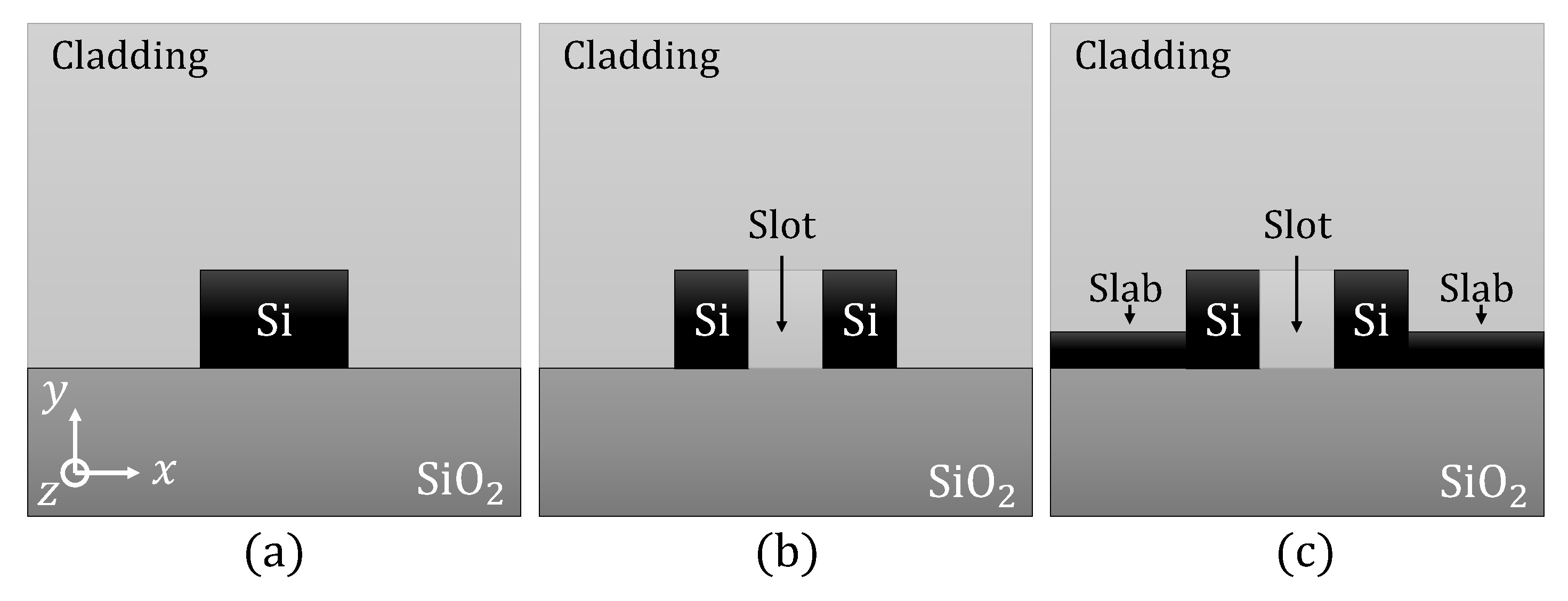
Silicon-on-insulator (SOI) wafers consist of a stack of crystalline silicon-substrate, a buried oxide (BOX) layer, a second silicon layer and a cladding top-layer. The cladding material can be air (), silicon dioxide () or an organic polymer (). In any case, the cladding material must have a lower refractive index than the silicon waveguide to ensure total internal reflection and thereby a guidance of the light wave. The purpose of the BOX-layer is to act as the lower cladding material. Furthermore, the BOX-layer has the advantage of less parasitic capacitance, which is crucial in high-speed modulator applications [17]. Figure 3 illustrates different kinds of integrated SOI waveguides, formed by etching of the silicon layer and enclosed by the deposition of a cladding material. While Figure 3a shows a conventional strip-waveguide, Figure 3b,c show two types of slot-waveguides, where the two silicon wires are separated by a slot (gap). The latter is responsible for a high optical field confinement and a high interaction with the EO slot material by the evanescent electric field of the propagating light. The slab in Figure 3c, also called strip-load, is used to contact the slot-waveguide to the electrodes of an EO-modulator device. With this application in mind, it is the configuration studied in this work. Furthermore, in case of SOH technology, PMMA+DR1 is deposited as the cladding material by spincoating into the slot region and covers the silicon wires and slabs [18].
2.3. Field Confinement Factor
To describe the interaction of light with the surrounding material, the field confinement factor is used as a figure of merit to characterize devices like slot-waveguides and their ability to confine an optical mode within a certain region [19]. The field confinement factor is defined as the ratio of the time averaged energy flow through the area of interest to the time averaged energy flow through the total area [20]
where and are the electric and magnetic field vectors, respectively, and is the unit vector in z (propagation) direction. Depending on the application, the area of interest is regarded differently. In EO modulators, it is the area of the slot region , where is most significant. Among others, the Pockels-effect enables the operation of EO modulators by inducing a refractive index change trough an applied electric field E:
where is the initial refractive index and the coefficient of the electro-optical tensor in the organic material. It becomes evident, that the factor , which ranges from , largely influences the strength of the Pockels-effect and thereby the modulation. In this work, the unperturbed refractive index is the refractive index of the polymer (Figure 2).
3. Simulation of Slot-Waveguides
To investigate the modal and confinement properties of a slot-waveguide we built a 2D finite element method (FEM)-based model in COMSOL Multiphysics®. The electromagnetic wave frequency domain (ewfd) has been chosen as the physics interface and the modal analysis was added to the study. For meshing the profile we used well over 3000 triangular vector-elements in a total area of = 5.0 µm × 2.5 µm, which was proven to give reliable and reproducible results. By calculating the eigenvalues and eigenfunctions of the Helmholtz equation
where is the wave number in free space and n is the refractive index of each material. Solving this equation gives the effective refractive index of the waveguide structure. The effective refractive index is an important property in modal analysis, because it describes impact of the waveguide on the optical mode in a single figure, without the need to resort to the electric fields, which cannot be measured directly anyway [21].
The slot-waveguide design and the denotation of its parameters is presented in Figure 4. Table 1 lists the parameters and their standard values, which are then consecutively varied to investigate the change in the effective refractive index and the field confinement factor. These values are widely used in literature due to their compatibility to typical SOI fabrication processes. The slot width s usually is the independent variable in this study.
During the design of the structure, only one half of the model has been drawn and afterwards mirrored on its vertical axis in a post-process. The waveguide wires are fully parameterized pentagonal Bézier-polygons, enabling a quick and flexible manipulation of the geometry. For the cladding material beneath, was used, while the wire waveguides and slabs consist of Si. For the cladding and slot material the dispersion curves of PMMA+DR1 were important into the program. All materials chosen from the database were measured at 293 K. The telecommunication wavelength was always fixed during the simulation.
4. Results
In this section the relative changes and absolute differences in the effective refractive index and the field confinement factor are presented for each mass concentration of the organic polymer. For each investigated parameter, the modal-field distribution from within COMSOL Multiphysics® are shown as an example. The term modal-field distribution is the visualization of the modal fields, i.e., the normalized electric field component of the electromagnetic wave for each waveguide mode. This is important for identifying regions with high and low field strength.
4.1. Non-Vertical Sidewalls
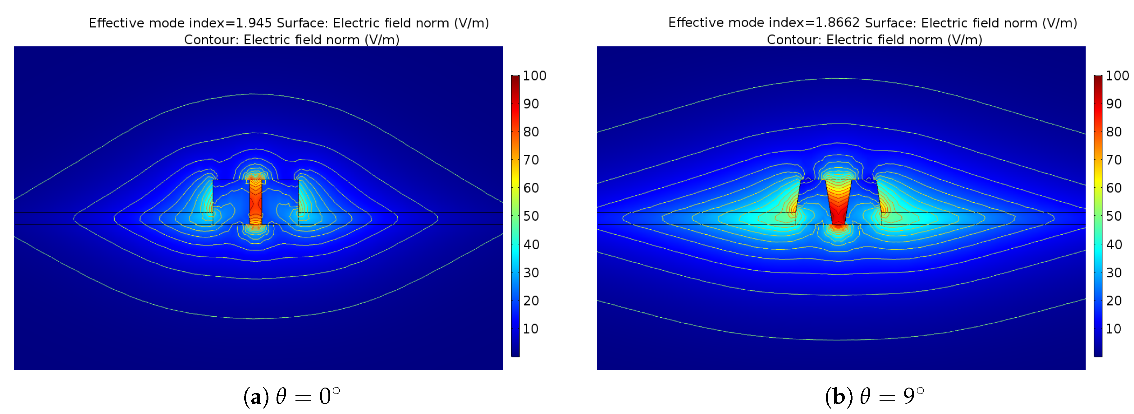
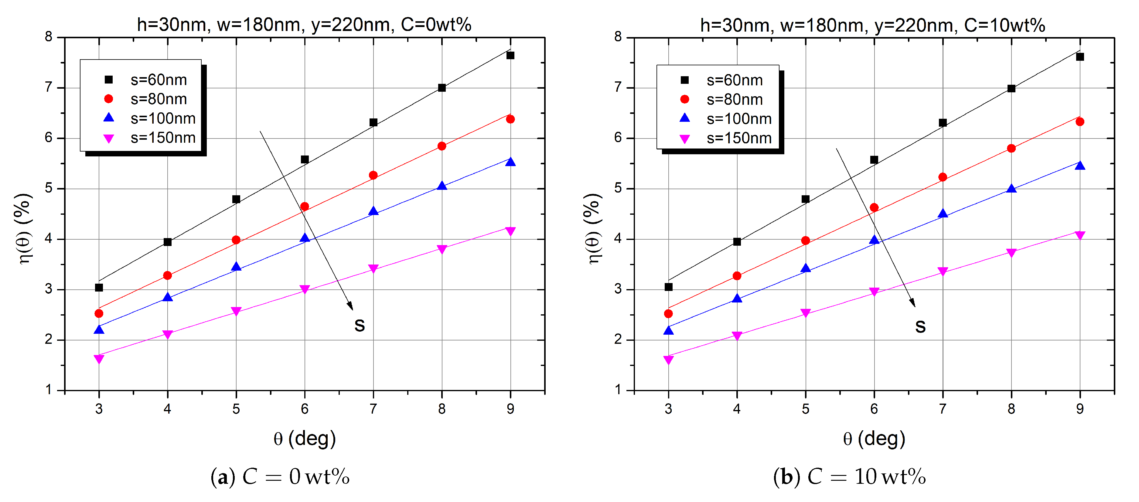
During the fabrication of slot-waveguides, silicon deep etching is applied in order to form the slot region. While doing so, it is often not possible to obtain perfectly vertical sidewalls. Therefore, the sidewalls will be tilted by an angle after etching. This obviously affects the modal-field distribution of the structure, visible in Figure 5. To take these manufacturing tolerances into account, we calculated the impact on the effective refractive index . A linear shift can be observed, increasing with the tilt angle . We defined the percentage of effective refractive index shift at a given tilt angle with respect to perfectly straight sidewalls by
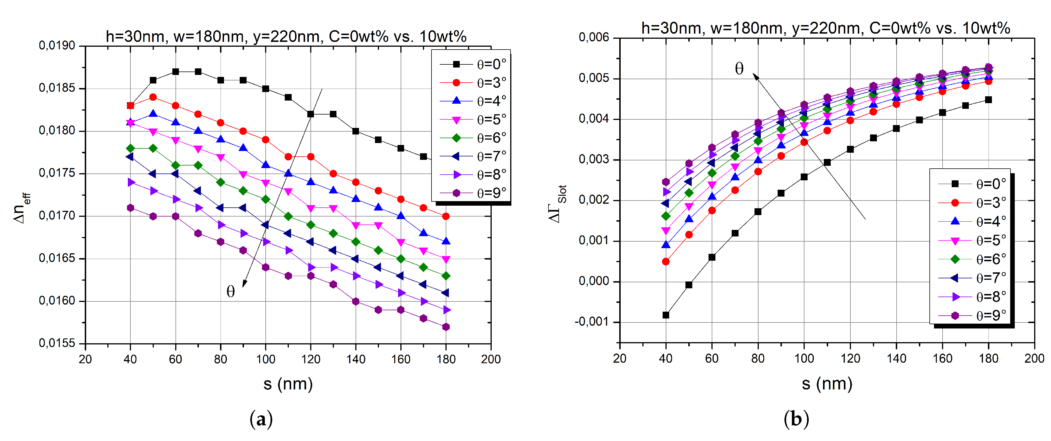
The change ranges from 1.6% to 7.9%, as shown in Figure 6. With increasing slot width s, the influence of the tilt angle becomes less pronounced, due to the relative large distance between the two silicon wires. Comparing Figure 6a,b shows that the difference between both concentration is negligible and, hence, the tilt angle has a more dominant effect on the effective refractive index.
The difference in the effective refractive index between the two concentrations and is given by
The results of our simulation study is shown in Figure 7a. There is a clear maximum at and = 0° of , while at an increasing tilt angle the behavior follows a linearly decreasing trend down to . For the confinement factor within the slot region , we find that it has a maximum of at and = 0°, from where it linearly decreases with s. However, considering the very low change of at its maximum and even negative values below , the influence of the tilt angle on the confinement factor appears negligible in Figure 7b.
4.2. Variation of the Waveguide Width
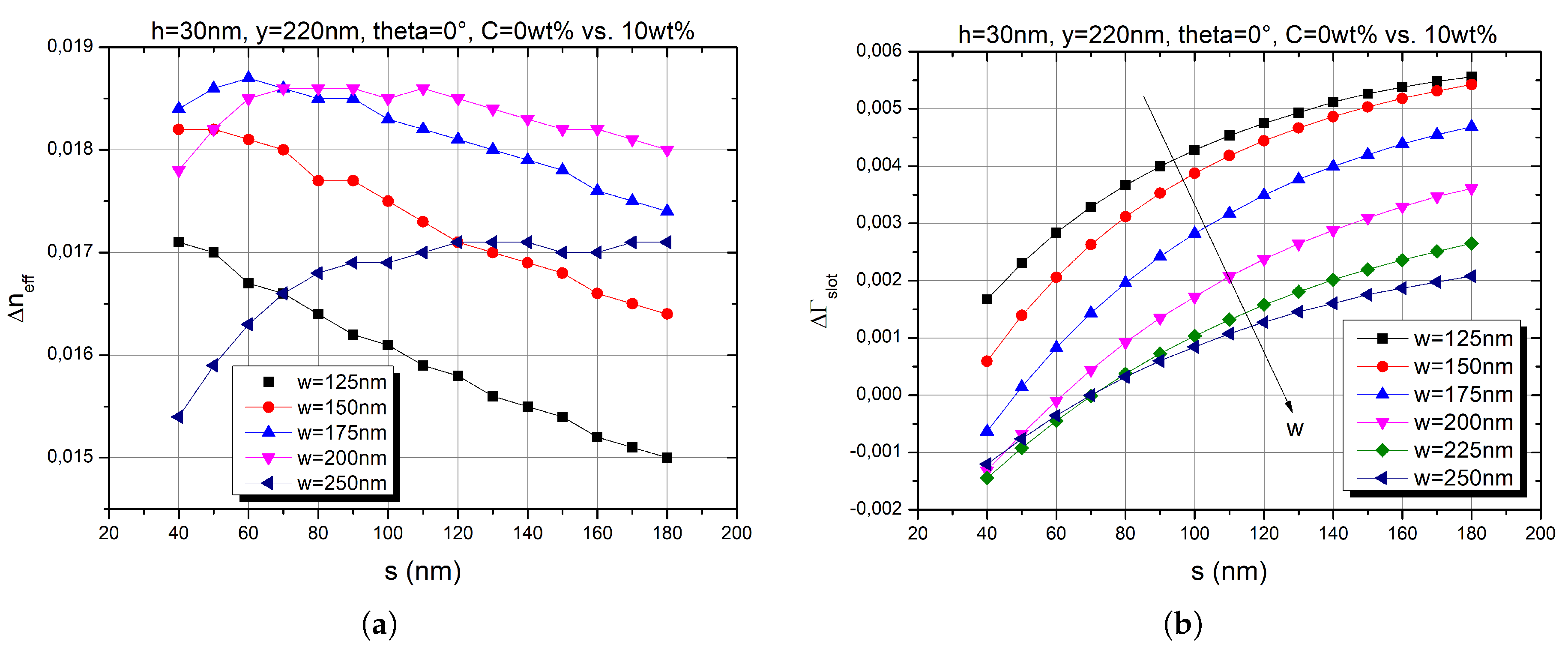
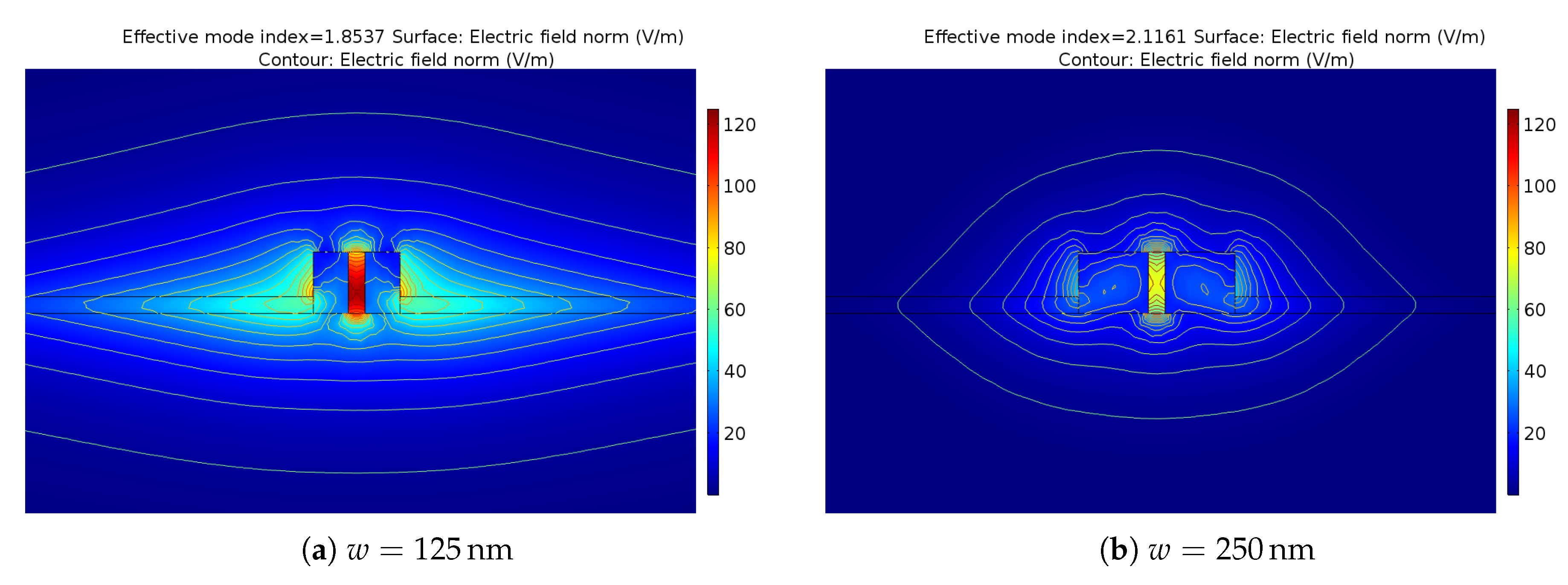
To find the optimal waveguide width w, we studied the changes in a range of to . An increase of w leads to higher values for , decreasing with the slot width s. However, regarding the difference in the effective index between the two concentrations, as shown in Figure 8a, we find a more complex relationship. While shows a maximum for at , it barely changes for over the entire range of s. A greater linear decrease becomes evident for and . In case of even an increase with s up to can be observed. The latter is due to the very wide waveguide wires, where the optical mode less likely enters the slot region, until a certain ratio of is overcome (Figure 9). For the entire range of w no higher modes were observed. A distinct maximum for has been found for and , up to . The difference is very small, though, and even becomes negative below , as shown in Figure 8b.
4.3. Influence of the Slab Height
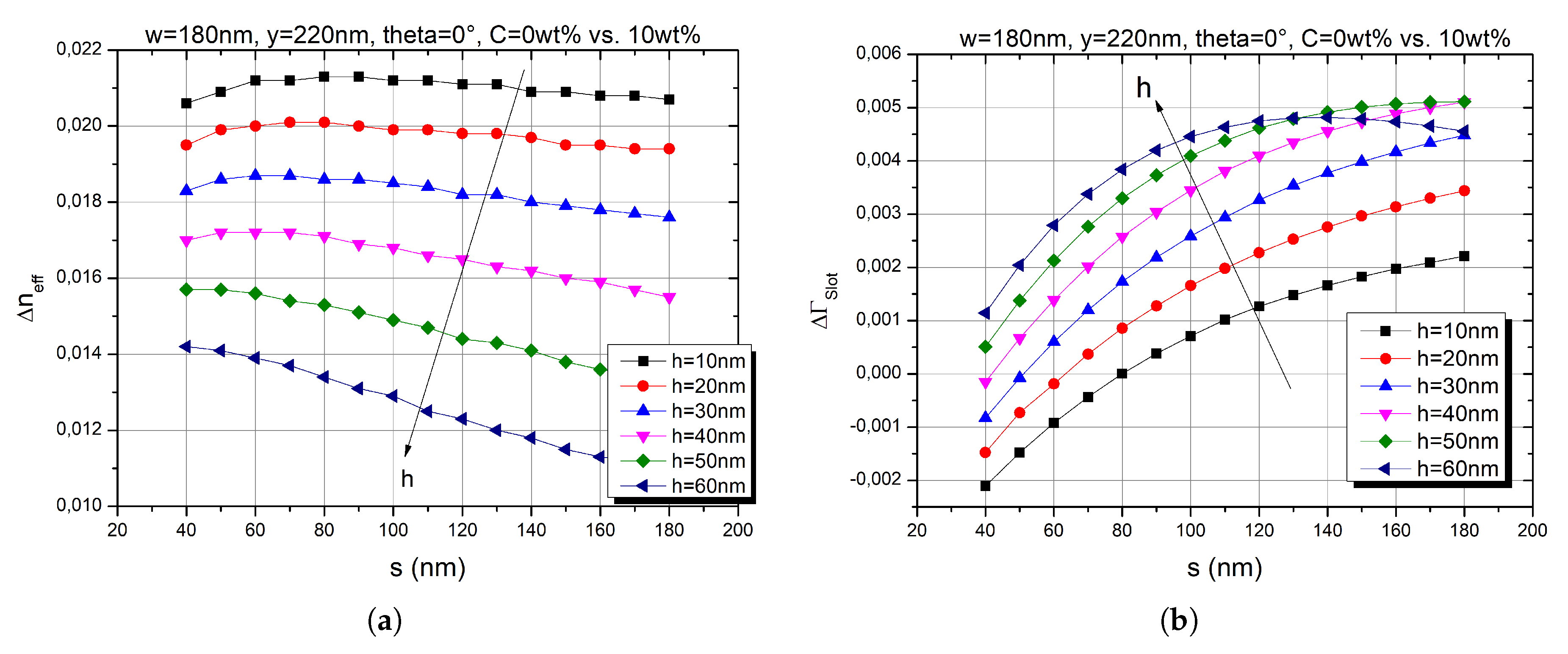
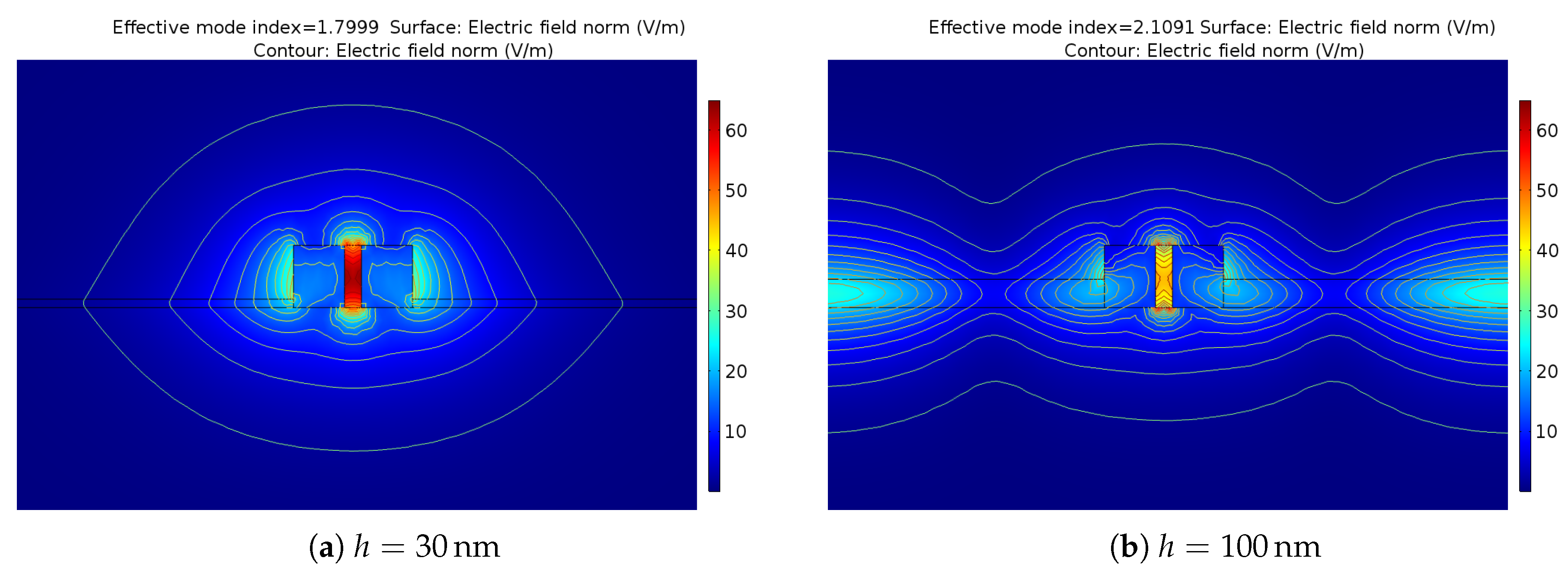
In EO modulators the slab is responsible for contacting the waveguide to the device, in order to apply an electric field to the slot and thereby changing the EO properties of the organic material. A greater slab height h leads to higher values for , while decreases and is more affected by s, presented in Figure 10a. During the simulation study we observed the propagation of higher modes starting from and shown as an extreme example for in Figure 11. This effect was already visible in Figure 10b at , where starts to drop. However, the manufacturing resolution and the electrical properties of the slab have to be taken into account for such small slab heights, which is why larger h become necessary.
In Appendix A we provide the raw data of our results; i.e., the effective refractive index and field confinement factor are plotted for each concentration. From these figures, optimized geometrical parameters for each concentration can be deduced, which are are summarized in Table 2. Please note that the general dependency on each parameter is the same for and and therefore the optimized values regarding field confinement factor are valid for both concentrations. It is also noticeable that field confinement factor is continuously increasing by decreasing the slab height. As a consequence, the slab height of is only the optimized value in our simulation but in general it holds that the smaller the slab height the higher the field confinement factor.
In summary, a thorough investigation on modal and confinement of silicon slot-waveguides covered by a nonlinear optical polymer has been performed. We calculated the effective refractive index and the field confinement factor for numerous geometry parameters of the slot-waveguide using a FEM-based 2D-model. As the cladding and slot material, the EO organic co-polymer PMMA+DR1 has been employed, which was taken from experimental data. Additionally, the resulting differences in the effective refractive index and field confinement factor between the two mass concentrations and of the DR1 chromophore in the PMMA matrix have been studied. In the first step we investigated the influence of non-vertical waveguide sidewalls, due to possible manufacturing tolerances during silicon etching. At = 0° and the highest confinement has been found. A linear percentual shift of from 1.6% to 7.9% has been observed with increasing tilt angle in a range of = 3°–9°. The influence was less pronounced for larger slot widths s. The difference between the two concentrations and ranged from 0.0157 up to 0.0187, while for the difference was negligible. Afterwards we varied the waveguide width w from to . A distinct maximum became visible at and . The difference stayed almost constant over the entire range of s for . No higher modes were observed. Finally, the influence of the slab height h was investigated. We found a maximum of at and . drops from onward, because the optical mode starts leaking into the silicon strip-load.
5. Conclusions
In this work, the influence of the dye concentration in a guest-host polymer system on the effective refractive index and field confinement of SOI slot-waveguides at various geometric parameters are investigated. It is shown that the dye concentration has a much weaker influence on both, the effective refractive index and the field confinement factor compared to the influence of the geometrical waveguide structure. As a consequence, the refractive index change due to different dye concentrations is negligible compared to the influence of geometrical parameters such as tilt angle, slot width and slab height. Our results can also be used as guideline for designing optimized silicon-organic hybrid slot-waveguides for electro-optical switches, modulators and tunable filter.
Author Contributions
P.S. and S.B. conceived and designed the simulation study; C.V. performed the material characterization; all authors analyzed the data.
Funding
This work is funded by European Regional Development Fund (10.13039/501100008530).
Acknowledgments
We acknowledge support by the German Research Foundation and the Open Access Publication Funds of the TH Wildau.
Conflicts of Interest
The authors declare no conflict of interest.
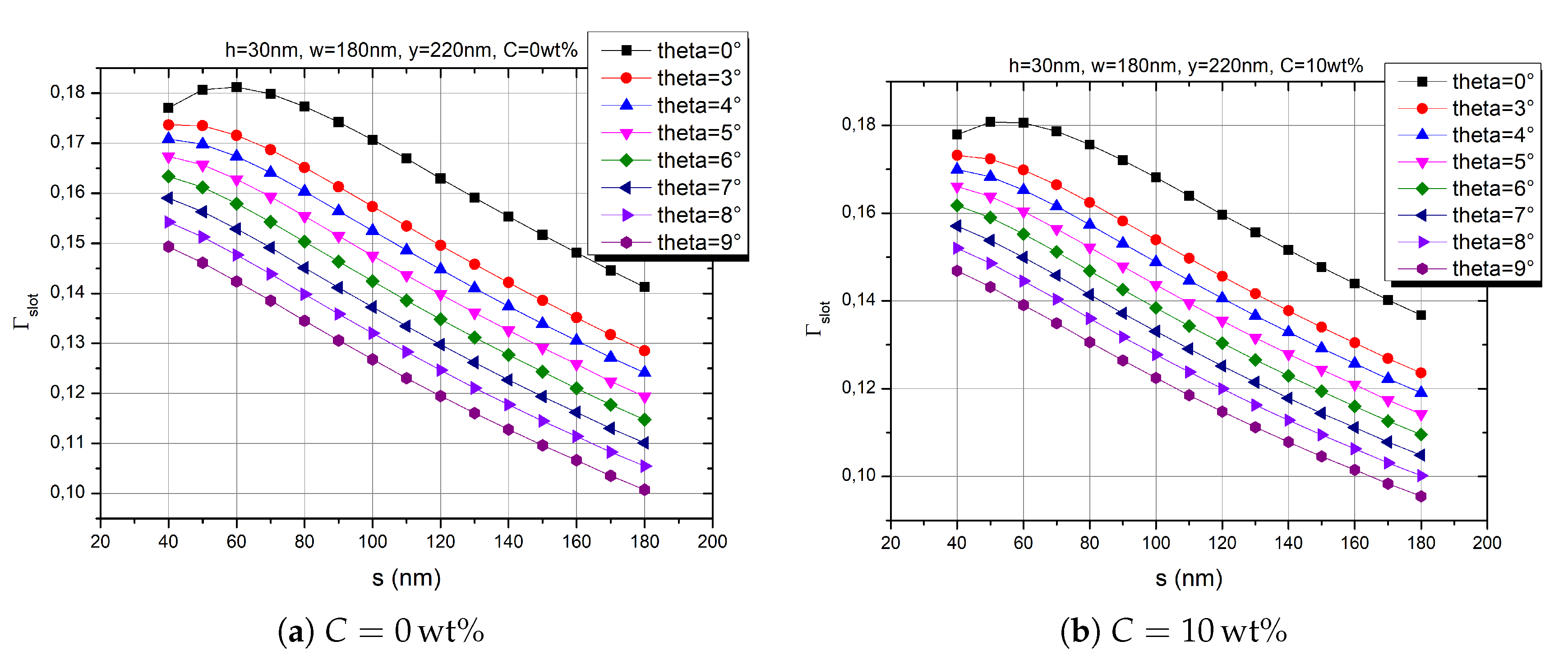
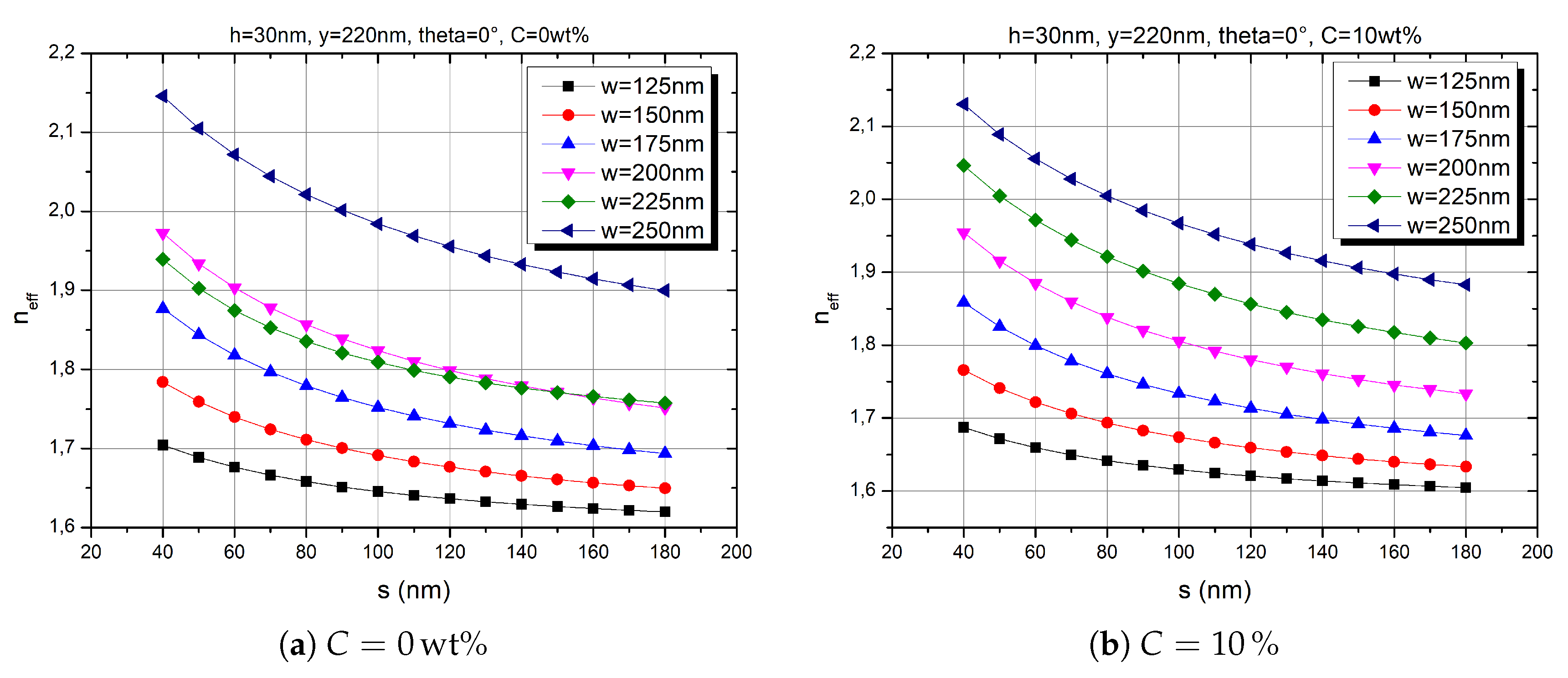
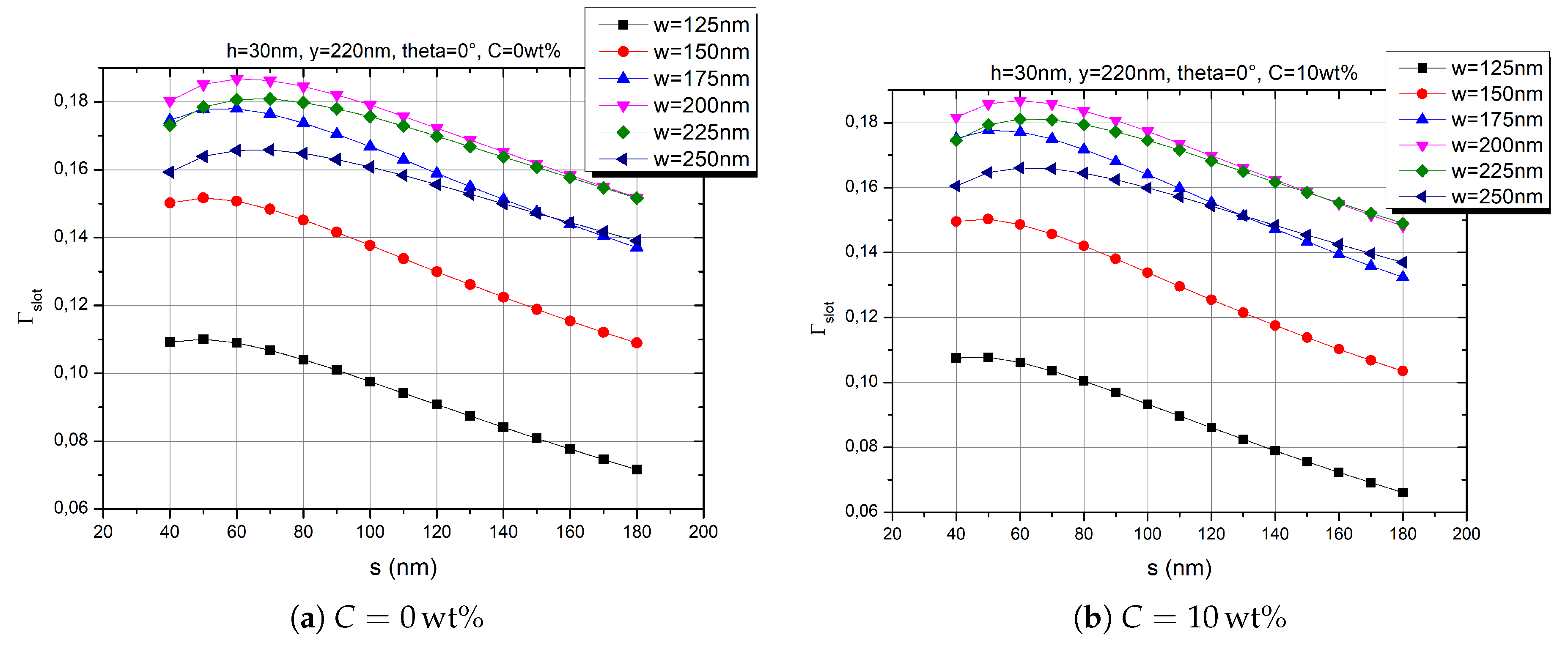
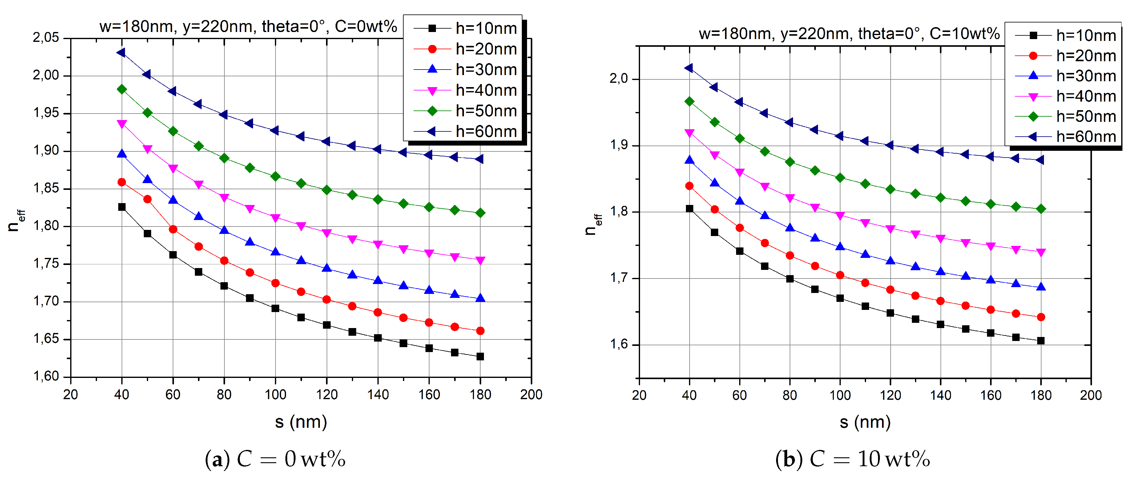
Appendix A. Raw Data
Figure A1.
Effective refractive index for both concentrations as a function of s and with as parameter.
Figure A1.
Effective refractive index for both concentrations as a function of s and with as parameter.

Figure A2.
Field confinement factor for both concentrations as a function of s and with as parameter.
Figure A2.
Field confinement factor for both concentrations as a function of s and with as parameter.

Figure A3.
Effective refractive index for both concentrations as a function of s and with w as parameter.
Figure A3.
Effective refractive index for both concentrations as a function of s and with w as parameter.

Figure A4.
Field confinement factor for both concentrations as a function of s and with w as parameter.
Figure A4.
Field confinement factor for both concentrations as a function of s and with w as parameter.

Figure A5.
Effective refractive index for both concentrations as a function of s and with h as parameter.
Figure A5.
Effective refractive index for both concentrations as a function of s and with h as parameter.

Figure A6.
Field confinement factor for both concentrations as a function of s and with h as parameter.
Figure A6.
Field confinement factor for both concentrations as a function of s and with h as parameter.

References
- Leuthold, J.; Koos, C.; Freude, W.; Alloatti, L.; Palmer, R.; Korn, D.; Pfeifle, J.; Lauermann, M.; Dinu, R.; Wehrli, S.; et al. Silicon-Organic Hybrid Electro-Optical Devices. IEEE J. Sel. Top. Quantum Electron. 2013, 19, 114–126. [Google Scholar] [CrossRef] [Green Version]
- Heni, W.; Kutuvantavida, Y.; Haffner, C.; Zwickel, H.; Kieninger, C.; Wolf, S.; Lauermann, M.; Fedoryshyn, Y.; Tillack, A.F.; Johnson, L.E.; et al. Silicon-Organic and Plasmonic-Organic Hybrid Photonics. ACS Photonics 2017, 4, 1576–1590. [Google Scholar] [CrossRef]
- Korn, D.; Palmer, R.; Yu, H.; Schindler, P.C.; Alloatti, L.; Baier, M.; Schmogrow, R.; Bogaerts, W.; Selvaraja, S.K.; Lepage, G.; et al. Silicon-organic hybrid (SOH) IQ modulator using the linear electro-optic effect for transmitting 16QAM at 112 Gbit/s. Opt. Express 2013, 21, 13219–13227. [Google Scholar] [CrossRef] [PubMed] [Green Version]
- Steglich, P.; Mai, C.; Villringer, C.; Pulwer, S.; Casalboni, M.; Schrader, S.; Mai, A. Quadratic electro-optic effect in silicon-organic hybrid slot-waveguides. Opt. Lett. 2018, 43, 3598–3601. [Google Scholar] [CrossRef] [PubMed]
- Kieninger, C.; Kutuvantavida, Y.; Elder, D.L.; Wolf, S.; Zwickel, H.; Blaicher, M.; Kemal, J.N.; Lauermann, M.; Randel, S.; Freude, W.; et al. Ultra-high electro-optic activity demonstrated in a silicon-organic hybrid modulator. Optica 2018, 5, 739–748. [Google Scholar] [CrossRef]
- Wolf, S.; Zwickel, H.; Hartmann, W.; Lauermann, M.; Kutuvantavida, Y.; Kieninger, C.; Altenhain, L.; Schmid, R.; Luo, J.; Jen, A.K.Y.; et al. Silicon-Organic Hybrid (SOH) Mach-Zehnder Modulators for 100 Gbit/s On-Off Keying. Sci. Rep. 2018, 8, 2598. [Google Scholar] [CrossRef] [PubMed]
- Steglich, P. Silicon-on-Insulator Slot Waveguides: Theory and Applications in Electro-Optics and Optical Sensing. In Emerging Waveguide Technology; You, K.Y., Ed.; IntechOpen: Rijeka, Croatia, 2018; Chapter 10. [Google Scholar] [CrossRef]
- Steglich, P.; Mai, C.; Stolarek, D.; Lischke, S.; Kupijai, S.; Villringer, C.; Pulwer, S.; Heinrich, F.; Bauer, J.; Meister, S.; et al. Novel ring resonator combining strong field confinement with high optical quality factor. IEEE Photonics Technol. Lett. 2015, 27, 2197–2200. [Google Scholar] [CrossRef]
- Steglich, P.; Mai, C.; Stolarek, D.; Lischke, S.; Kupijai, S.; Villringer, C.; Pulwer, S.; Heinrich, F.; Bauer, J.; Meister, S.; et al. Partially slotted silicon ring resonator covered with electro-optical polymer. Proc. SPIE 2016, 9891, 98910R. [Google Scholar] [CrossRef]
- Zhang, J.; Cassan, E.; Gao, D.; Zhang, X. Highly efficient phase-matched second harmonic generation using an asymmetric plasmonic slot waveguide configuration in hybrid polymer-silicon photonics. Opt. Express 2013, 21, 14876–14887. [Google Scholar] [CrossRef] [PubMed]
- Falco, A.D.; Conti, C.; Assanto, G. Quadratic phase matching in slot waveguides. Opt. Lett. 2006, 31, 3146–3148. [Google Scholar] [CrossRef] [PubMed] [Green Version]
- Wrana, C. Polymerphysik: Eine Physikalische Beschreibung von Elastomeren und Ihren Anwendungsrelevanten Eigenschaften; Springer: Berlin/Heidelberg, Germany, 2014. [Google Scholar]
- Dalton, L.R.; Günter, P.; Jazbinsek, M.; Sullivan, P.A.; Kwon, O.P. Organic Electro-Optics and Photonics: Molecules, Polymers and Crystals; Cambridge University Press: Cambridge, UK, 2015. [Google Scholar]
- Vivien, L.; Pavesi, L. Handbook of Silicon Photonics; Taylor & Francis: Abingdon, UK, 2016. [Google Scholar]
- Palmer, R.; Koeber, S.; Elder, D.; Woessner, M.; Heni, W.; Korn, D.; Lauermann, M.; Bogaerts, W.; Dalton, L.; Freude, W.; et al. High-Speed, Low Drive-Voltage Silicon-Organic Hybrid Modulator Based on a Binary-Chromophore Electro-Optic Material. Lightwave Technol. J. 2014, 32, 2726–2734. [Google Scholar] [CrossRef] [Green Version]
- Weber, M. Handbook of Optical Materials; Laser & Optical Science & Technology; Taylor & Francis: Abingdon, UK, 2002. [Google Scholar]
- Celler, G.; Cristoloveanu, S. Frontiers of silicon-on-insulator. J. Appl. Phys. 2003, 93, 4955–4978. [Google Scholar] [CrossRef]
- Palmer, R.; Koeber, S.; Woessner, M.; Elder, D.L.; Heni, W.; Korn, D.; Yu, H.; Lauermann, M.; Bogaerts, W.; Dalton, L.R.; et al. High-speed silicon-organic hybrid (soh) modulators with 230 pm/v electro-optic coefficient using advanced materials. In Optical Fiber Communication Conference; Optical Society of America: Washington, DC, USA, 2014; Paper M3G.4. [Google Scholar]
- Steglich, P.; Villringer, C.; Pulwer, S.; Casalboni, M.; Schrader, S. Design Optimization of Silicon-on-Insulator Slot-Waveguides for Electro-optical Modulators and Biosensors. In Photoptics 2015; Ribeiro, P., Raposo, M., Eds.; Springer Proceedings in Physics; Springer International Publishing: Cham, Switzerland, 2016; Chapter 11; pp. 173–187. [Google Scholar]
- Steglich, P.; Villringer, C.; Dümecke, S.; Michel, Y.P.; Casalboni, M.; Schrader, S. Silicon-on-Insulator Slot-waveguide Design Trade-offs. In Proceedings of the International Conference on Photonics, Optics and Laser Technology (PHOTOPTICS), Berlin, Germany, 13–15 March 2015; Volume 2, pp. 47–52. [Google Scholar] [CrossRef]
- Reed, G.; Knights, A. Silicon Photonics: An Introduction; Wiley: Hoboken, NJ, USA, 2004. [Google Scholar]
Figure 1.
Chemical structure of the organic chromophore DR1 (left) and the polymer PMMA (right) employed as the EO medium.
Figure 1.
Chemical structure of the organic chromophore DR1 (left) and the polymer PMMA (right) employed as the EO medium.

Figure 2.
Dispersion curves of PMMA+DR1 for different mass concentrations C of the contained DR1 chromophore, where n is the refractive index and the extinction coefficient.
Figure 2.
Dispersion curves of PMMA+DR1 for different mass concentrations C of the contained DR1 chromophore, where n is the refractive index and the extinction coefficient.

Figure 3.
Cross sections of (a) conventional strip-waveguides, (b) slot-waveguides and (c) a slot-waveguide with slabs. The latter is the configuration studied in this work.
Figure 3.
Cross sections of (a) conventional strip-waveguides, (b) slot-waveguides and (c) a slot-waveguide with slabs. The latter is the configuration studied in this work.

Figure 4.
Enlarged section of the slot-waveguide’s design and denotation of its parameters. A large tilt angle = 9° has been used for better visibility.
Figure 4.
Enlarged section of the slot-waveguide’s design and denotation of its parameters. A large tilt angle = 9° has been used for better visibility.

Figure 5.
Influence of sidewall tilt angle on the modal properties. It becomes visible that confinement of the optical mode decreases with larger angle.
Figure 5.
Influence of sidewall tilt angle on the modal properties. It becomes visible that confinement of the optical mode decreases with larger angle.

Figure 6.
Percentual shift in effective refractive index over the tilt angle of both concentrations, with slot width s as parameter.
Figure 6.
Percentual shift in effective refractive index over the tilt angle of both concentrations, with slot width s as parameter.

Figure 7.
Difference in the effective refractive index (a) and the field confinement factor (b) of both concentrations as a function of s, with as parameter.
Figure 7.
Difference in the effective refractive index (a) and the field confinement factor (b) of both concentrations as a function of s, with as parameter.

Figure 8.
Difference in the effective refractive index (a) and the field confinement factor (b) of both concentrations as a function of s, with w as parameter.
Figure 8.
Difference in the effective refractive index (a) and the field confinement factor (b) of both concentrations as a function of s, with w as parameter.

Figure 9.
Effect of the waveguide width w on the modal properties. A higher confinement can be found for larger w.
Figure 9.
Effect of the waveguide width w on the modal properties. A higher confinement can be found for larger w.

Figure 10.
Difference in the effective refractive index (a) and the field confinement factor (b) of both concentrations as a function of s, with h as parameter.
Figure 10.
Difference in the effective refractive index (a) and the field confinement factor (b) of both concentrations as a function of s, with h as parameter.

Figure 11.
Influence of the slab height h on the modal properties. Higher modes propagating into the slab can be found for .
Figure 11.
Influence of the slab height h on the modal properties. Higher modes propagating into the slab can be found for .


Table 1.
Slot-waveguide parameters and their standard values.
| Symbol | Parameter | Standard Value |
|---|---|---|
| tilt angle | 0° | |
| w | waveguide width | |
| y | waveguide height | |
| h | slab height | |
| s | slot width | variable |
| wavelength |
Table 2.
Optimized slot-waveguide parameters in terms of field confinement factor.
| Symbol | Parameter | Optimized Value |
|---|---|---|
| tilt angle | 0° | |
| w | waveguide width | |
| h | slab height | |
| s | slot width |
© 2018 by the authors. Licensee MDPI, Basel, Switzerland. This article is an open access article distributed under the terms and conditions of the Creative Commons Attribution (CC BY) license (http://creativecommons.org/licenses/by/4.0/).
Share and Cite
MDPI and ACS Style
Bondarenko, S.; Villringer, C.; Steglich, P. Comparative Study of Nano-Slot Silicon Waveguides Covered by Dye Doped and Undoped Polymer Cladding. Appl. Sci. 2019, 9, 89. https://doi.org/10.3390/app9010089
AMA Style
Bondarenko S, Villringer C, Steglich P. Comparative Study of Nano-Slot Silicon Waveguides Covered by Dye Doped and Undoped Polymer Cladding. Applied Sciences. 2019; 9(1):89. https://doi.org/10.3390/app9010089
Chicago/Turabian StyleBondarenko, Siegfried, Claus Villringer, and Patrick Steglich. 2019. "Comparative Study of Nano-Slot Silicon Waveguides Covered by Dye Doped and Undoped Polymer Cladding" Applied Sciences 9, no. 1: 89. https://doi.org/10.3390/app9010089
Note that from the first issue of 2016, this journal uses article numbers instead of page numbers. See further details here.