Stochastic Effects on the Dynamics of the Resonant Structure of a Lorentz Force MEMS Magnetometer


1
College of Engineering, School of Mechanical Engineering, University of Tehran, North Kargar St., Tehran, P.O. Box 14399-55961, Iran
2
Dipartimento di Ingegneria Civile e Ambientale, Politecnico di Milano, Piazza L. da Vinci 32, 20133 Milano, Italy
*
Author to whom correspondence should be addressed.
Actuators 2019, 8(2), 36; https://doi.org/10.3390/act8020036
Submission received: 15 March 2019
/
Revised: 17 April 2019
/
Accepted: 25 April 2019
/
Published: 30 April 2019
(This article belongs to the Special Issue Instability Phenomena and Complex Responses in Electrically-Actuated Microbeam-Based MEMS)
Abstract
:Resonance features of slender mechanical parts of Lorentz force MEMS magnetometers are affected by the (weakly) coupled thermo-electro-magneto-mechanical multi-physics governing their dynamics. We recently showed that reduced-order models for such parts can be written in the form of the Duffing equation, whose nonlinear term stems from the mechanical constraint on the vibrations and is affected by the driving voltage. As some device performance indices vary proportionally to the amplitude of oscillations at resonance, an optimization of the operational conditions may lead to extremely slender, imperfection-sensitive movable structures. In this work, we investigate the effects of imperfections on the mechanical response of a single-axis magnetometer. At the microscopic length-scale, imperfections are given in terms of uncertainties in the values of the over-etch depth and of the Young’s modulus of the vibrating polycrystalline silicon film. Their effects on the nonlinear structural dynamics are investigated through a Monte Carlo analysis, to show how the output of real devices can be scattered around the reference response trend.
1. Introduction
The rapid development of semiconductor technologies has enabled the mass production of plenty of micro electrical-mechanical system (MEMS) devices [1,2,3], among which the magnetometers considered in this study are relevant for compass applications. To design and predict the performance of these micro-devices, accurate models are required to account for the interaction among various physical fields, primarily the thermal, electric, magnetic, and mechanical ones. Numerical and analytical methods have been recently proposed to understand the underlying working principles, and increase the capability to match experimental evidences [4,5,6,7].
Standard approaches typically assume that the geometrical and physical properties of the device are known in a deterministic sense. In reality, especially with a view towards the goal of progressively reducing the device footprint, uncertainties look unavoidable and may become dominant due to a variety of factors linked to the micro-fabrication process [8]. For polysilicon MEMS, in [9,10,11,12,13,14] the effects of the crystalline morphology on the reliability of inertial devices subjected to impacts were studied. At the scale of the full device, it turned out that marginal effects can be actually reported regarding the failure mode, if any, as induced by micro-cracking of silicon. Looking instead more closely to the details of crack initiation and final percolation throughout the structural parts, small deviations may discriminate between failure and no-failure outcomes in different devices, which may differ only in terms of the film morphology in the failing region. Such result was validated against real experimental data [10].
Focusing on the operational conditions of micro-devices, an on-chip test procedure was proposed in [15,16]. To avoid accounting for the additional effects of residual stresses possibly induced by micro-fabrication, the movable structure was purposely designed as statically determinate. By slightly varying the geometry of the tested polysilicon samples and the actuation/sensing setup, the superposed effects of the polycrystalline elastic and geometric properties on the structural stiffness and, therefore, on the device response to actuation were assessed. Data reduction also provided a quantitative measure of the stochastic variability of Young’s modulus of the polysilicon film, and of the over-etch depth [17,18].
Along the same line and with the aim to extend the preliminary results reported in [19], we deal here with the operational conditions of a single-axis (z-axis) Lorentz force MEMS magnetometer. As anticipated, this type of magnetometer has been developed for low-power electronic compass applications in handheld devices (see, e.g., [4,20,21,22]). For this purposes, the MEMS must be able to sense the Earth’s magnetic field, which amounts at most to about 100 μT. Indeed, sensitivity is not the only performance index to account for in the design, since power consumption is of paramount importance for mobile applications. In this regard, a so-called balanced optimization scheme was proposed in [6,7] to allow also for bandwidth and resolution of a capacitive, single-axis Lorentz force magnetometer similar to that here considered, see also [23,24,25].
To model the dynamics of the magnetometer resonant structure, which consists of a slender beam in a clamped-clamped configuration, the weak interaction among the thermal, electric, magnetic, and mechanical fields must be accounted for. The electric and magnetic fields interact to provide the Lorentz force inducing in-plane beam deformations, or vibrations in the case of a time-varying electric field flowing longitudinally in the beam. The Joule effect leads to a temperature rise in the beam that, being constrained at both ends, has a tendency to buckle if a critical threshold is attained. Though this instability has to be avoided, like pull-in under operational conditions, its proximity can be exploited to enhance the amplitude of oscillations, until a safe limit, and to simultaneously tune the working frequency of the device. A simplified model of this multi-physics frame has been developed by assuming a specific deformation mode for the beam, driven by its geometry and constraints. The differential equation governing the motion of the beam finally results to be of a Duffing type, where both the linear and nonlinear (cubic) stiffness terms embed the effects of the multi-physics, showing softening effects linked to the thermal load and to the electrostatic forces due to sensing. Uncertainties have been embedded by allowing for the scattered values of the Young’s modulus and over-etch depth (see [15]) in a batch of statistically representative samples. To assess the effects of those uncertainty sources on the overall performance of the device, a series of Monte Carlo simulations has been run. Granted that the outcomes of this stochastic analysis cannot be automatically extended to any geometry, it is shown that over-etch has a greater impact on the solution, since it affects all the structural characteristics of the vibrating beam. In some cases, it may provide a geometry more prone to buckling, thus approaching the upper bounds on performance indicators whenever they are proportional to the compliance of the structure. Overall, if the compliance is maximized along with its effects on the (capacitive) sensing, the repeatability from part to part can be adversely affected and calibration becomes necessary to avoid drifts and biases [26,27]. Very recently, the proposal to embed machine learning capabilities into real-world devices has emerged as a disrupting trend (see, e.g., [28]); to train the neural network possibly driving a classifier, an approach can rely upon a simple stochastic model, like the one here proposed. Therefore, handling geometrical and mechanical parameters at the micro-scale in a statistical fashion looks necessary, as well as to develop a kind of embedded artificial intelligence for next generation devices.
The remainder of the paper is organized as follows: In Section 2, the multi-physics governing the problem is discussed in details and, moving from a weak form of energy conservation, the reduced-order model is obtained. To feed the stochastic analyses with data relevant to the scattering in the effective Young’s modulus of the beam, a numerical homogenization procedure is discussed in Section 3. The results of Monte Carlo simulations, preceded by a sensitivity analysis, are collected in Section 4. Finally, Section 5 is aimed at highlighting the main achievements of the current work, and foreseeing future developments to avoid the approximations introduced here to simplify the analysis.
2. A Reduced-Order Model of the Resonating Structure
Different geometries were proposed for the resonating structures of Lorentz force MEMS magnetometers, each one specifically tailored for one-, two-, or three-axis compass applications (see, e.g., [4,29]). In this work, we focus on the configuration depicted in Figure 1: the movable parts of this MEMS are represented by a series of mechanically independent slender beams, connected to the substrate at their end cross-sections. Each beam carries a couple of plates for sensing purposes; to prevent as much as possible any global (rigid body-like) tilting mode due to asymmetric imperfections, such plates are connected to the mid-span cross-section of the beam. The considered device is able to sense a magnetic field aligned with the out-of-plane direction (, according to the adopted reference frame), by exploiting the in-plane motion of the beam and, therefore, of the sensing plates.
The analysis to follow refers to a single beam, featuring length and a rectangular cross-section of area , being the in-plane width and the out-of-plane thickness. Due to the end constraints, the beam vibrates in a clamped-clamped configuration.
In accordance with the micro-fabrication process, see e.g., [8], the beam is assumed to be made of a polycrystalline silicon film with a columnar structure. For the present analysis the length is assumed to be large enough, in comparison with a characteristic size of the polycrystalline morphology, to avoid considering local or higher-order effects on the dynamic properties of the beam. The beam is, therefore, assumed to be homogeneous, and the elastic properties governing its in-plane vibrations can be obtained through homogenization over a statistical volume element (SVE) of the polysilicon film; additional details are provided in Section 3.
As the beam is constrained at both ends, softening induced by thermal effects and driving voltage modifies the frequency at which the maximum amplitude of the vibrations is sensed. Out of the operational conditions, by increasing, e.g., the current density flowing in the flexure (see below), vibrations can be further amplified and buckling might get incepted; if the device is appropriately designed to enforce a small amplitude of the oscillations, pull-in instability [30] could be instead easily avoided. The elastic response of the beam is thus modeled accounting for second-order effects, see [31,32,33], so that the lateral deflection does affect the equilibrium state. Due to the beam slenderness, as measured by the ratio , energy conservation is enforced in weak form through:
where the integrals respectively denote the first-order and second-order terms of the internal energy, the kinetic energy and the work of external forces. In Equation (1), that must hold for any variation of the beam deflection and of the relevant space and time derivatives, an Euler-Bernoulli kinematics has been enforced, so that beam cross-sections are always assumed to maintain their planar geometry and their orthogonality with the deflected longitudinal axis. Terms appearing in the conservation law are: , being time, is the beam deflection; space derivatives and represent the rotation and the curvature of the beam axis; time derivative represents the lateral acceleration; is the flexural rigidity of the beam, being the effective in-plane polysilicon Young’s modulus and the moment of inertia of the beam cross-section; is the mass per unit length, being the mass density; is the axial load, positive if tensile, caused by thermal effects; and is the magnitude of the lateral load per unit length, due to the external actions.
The energy conservation equation is solved by imposing that the beam deflection can be written as:
thereby assuming in the solution a multiplicative decomposition into space and time functions. The resulting single degree of freedom represents the time evolution of the amplitude of oscillations at the mid-span cross-section. The differential equation governing the time evolution of can then be recast in the form of Duffing equation, as follows:
where:
Terms in Equation (4) respectively represent the effective mass, damping, linear, and cubic stiffness, and external load (Lorentz force) ones, see also [34]. In these equations: is the mass per unit length of the attached sensing plates, which might be different from if beam and plates are designed to have different in-plane widths; is the effective viscosity coefficient of the surrounding air; is the gap between the two surfaces of each parallel-plate capacitor; is the coefficient of (longitudinal) thermal expansion; is the density of the current, flowing longitudinally in the beam; is the mid-span temperature raise due to Joule effect; is the driving voltage; is the permittivity of vacuum; and is the magnitude of the out-of-plane magnetic field to be sensed.
In this formulation, as proposed in [5], the mass term accounts for the contribution of the two sensing plates too, as they move together with the beam and behave like rigid bodies to interact with the massive stators at top and bottom sides, see Figure 1. The damping term is given by the squeeze of the fluid at the sensing electrodes, see [3,35]. As for the stiffness terms and , the aforementioned softening effects are measured by the temperature raise caused by the Joule effect, and by the electrostatic forces at the parallel plate capacitors. An increase of the current density or of the driving voltage may, thus, increase the amplitude of oscillations, and also the sensitivity to imperfections in the response of the device. Instability phenomena, like mechanical buckling or pull-in, must be avoided under operational conditions: in [5], a trade-off was automatically set in between increasing the magnetometer performances and decreasing the risk of instabilities, by constraining the resonance frequency of the movable structure within a standard range for this type of applications.
In the Duffing equation (Equation (3)), the term quantifies the deviation from linearity in the system dynamics. As it is affected by (see Equation (4)), the relevant dependency on the driving mechanism needs to be accurately assessed in the solution. We then assume that the forcing term varies according to , where is the corresponding frequency; the maximum amplitude of the oscillations is then provided as the solution of the following equation [32]:
where is the natural frequency relevant to the linearized beam response.
The analytical solution of Equation (5) for was already discussed in [5]. The main point to stress here is that such solution obviously depends on and which, in turn, depend on the flexural and axial rigidities of the beam. Hence, uncertainties in the values of the polysilicon Young’s modulus and of the beam width induce a scattering in the value of , that has to be properly quantified at the design stage. For this purpose, in what follows, we provide a model to account for the aforementioned uncertainties at the polycrystalline level. For what concerns the Young’s modulus of the micro-structured silicon film, results of stochastic homogenization are discussed in Section 3. As the width of the film depends on the over-etch depth induced by the micro-fabrication process (see [15,16,17]) a discussion pertinent to this effect is provided in Section 4.
3. Effective Elastic Properties of the Polysilicon Film
In the formulation provided in Section 2, the elastic properties of the polysilicon film come explicitly into play through the Young’s modulus in the longitudinal direction . Though not accounted for here, the out-of-plane beam thickness or, effectively, the ratio between this thickness and the in-plane beam width , may lead to plain strain conditions to hold in the micro-structured film; the bending stiffness should be therefore appropriately modified, to account for the additional effect of the Poisson’s ratio on the deformation field.
As the stochastic effects of the polycrystalline morphology on the elastic moduli of the film have to be evaluated, we propose two different strategies to obtain quantitative estimations. A former one is aimed at bilaterally bounding the asymptotic solution for samples of the film featuring a size growing to infinity; this is obtained through an analytical homogenization procedure. A latter one is instead aimed at assessing the morphology-induced scattering in the solution for the finite size beam geometry under consideration, and is obtained via a Monte Carlo-driven, numerical homogenization procedure. The two approaches were already adopted in [36] (see also [14]), and they are briefly discussed in what follows to assure a self-consistent description of the whole method.
In both procedures, we account for the columnar micro-structure of the epitaxially grown polycrystalline silicon film. To simplify the analysis, we assume that a texture is aligned with the out-of-plane direction, namely is perpendicular to the substrate: therefore, homogenization is carried out in the plane only (see Figure 1) and two-dimensional digital representations of the film morphology are adopted in the analysis. As detailed in several studies (see e.g., [8,9]) this assumption looks appropriate for the considered micro-fabrication process, leading to a sub-vertical growth of all the silicon grains.
3.1. Analytical, Deterministic Homogenization
As anticipated, bounds obtained with this approach are valid asymptotically, for a ratio between the in-plane dimensions of the polysilicon sample and the characteristic grain size (or radius) tending to infinity. The procedure is therefore intended to provide bilateral bounds on the mean values of the Young’s modulus of polysilicon, since bounds result to be too tight if the ratio between a characteristic size of the beam, like its width , and does not take large values.
Bounds on the elastic moduli are based on the Voigt and Reuss approaches, which assume that either the strain or stress state is uniform throughout the polycrystalline sample [37]. Moving from the Hill-Mandel macro-homogeneity condition, under the Voigt assumption of a uniform strain field, the effective stiffness matrix is bounded by:
Under the Reuss assumption of a uniform stress field, the following bound on the effective compliance matrix is instead obtained:
In these equations: is (the measure of) the polysilicon sample volume that is, in the present two-dimensional case, the in-plane area; is the in-plane single-crystalline silicon stiffness matrix in a local reference frame aligned with the axes of elastic symmetry, which reads:
where GPa, GPa and GPa (see, e.g., [9]); and are the orthogonal transformation matrices, that allow to respectively transform the stress and strain vectors from the global reference frame of Figure 1 to the local one aligned with the aforementioned axes of elastic symmetry. According to a standard notation, superscripts and respectively refer to the transpose and to the inverse of the relevant matrices.
To compute the bounds, we assume that the in-plane lattice orientation of each grain is a fluctuating field with a uniform statistical distribution. The integral over in Equations (6) and (7) can, therefore, be transformed into an integral over such random orientation. The resulting overall behavior of the polysilicon film turns out to be in-plane isotropic, with bounds on the Young’s modulus given by: GPa, as furnished by the Voigt method; GPa, as furnished by the Reuss method.
The assumption of a uniform distribution for the lattice orientation was already proved to fail in case of real film geometries, like those here considered, since the number of grains in the film sample is not large enough [38]. Therefore, the study to follow is aimed at providing a stochastic description of the scattering in the beam stiffness.
3.2. Numerical, Stochastic Homogenization
In the current work, the length-scale separation principle [39] adopted to define the properties of a representative volume element of the polycrystalline film does not hold true, due to the small values of the ratio. Because of the expected growth of the effects on the results of micro-structural features of the polycrystalline morphology, an SVE is adopted to feed a Monte Carlo procedure aiming to estimate the scattering in the Young’s modulus of the film, see Figure 2. Perturbations on the SVE geometry are provided in terms of topology of the grain boundary network, and in terms of in-plane orientation of the symmetry axes of each silicon grain.
Each micro-structured sample is numerically generated using a (regularized) Voronoi tessellation, see [9,14,36], wherein a target grain size is assumed. To bound the elastic response of each SVE, either uniform strain of uniform stress boundary conditions (BCs) are adopted. The mentioned BCs are aimed to define the displacement or the traction field along the lateral boundary of the SVE, and do not provide any additional constraint on the local stress and strain fields inside. The overall SVE response is computed by defining the macroscopic stress and strain vectors as the volume integrals of the relevant microscopic, fluctuating fields, and by linking them linearly through , where is the same stiffness matrix considered before and in need of an estimation. To compute the entries of , a procedure was proposed in [36] on the basis of a set of finite element simulations, each one featuring only one component of either or different from zero, depending on the type of BCs handled. Procedural details are omitted here, and interested readers can find them in [36].
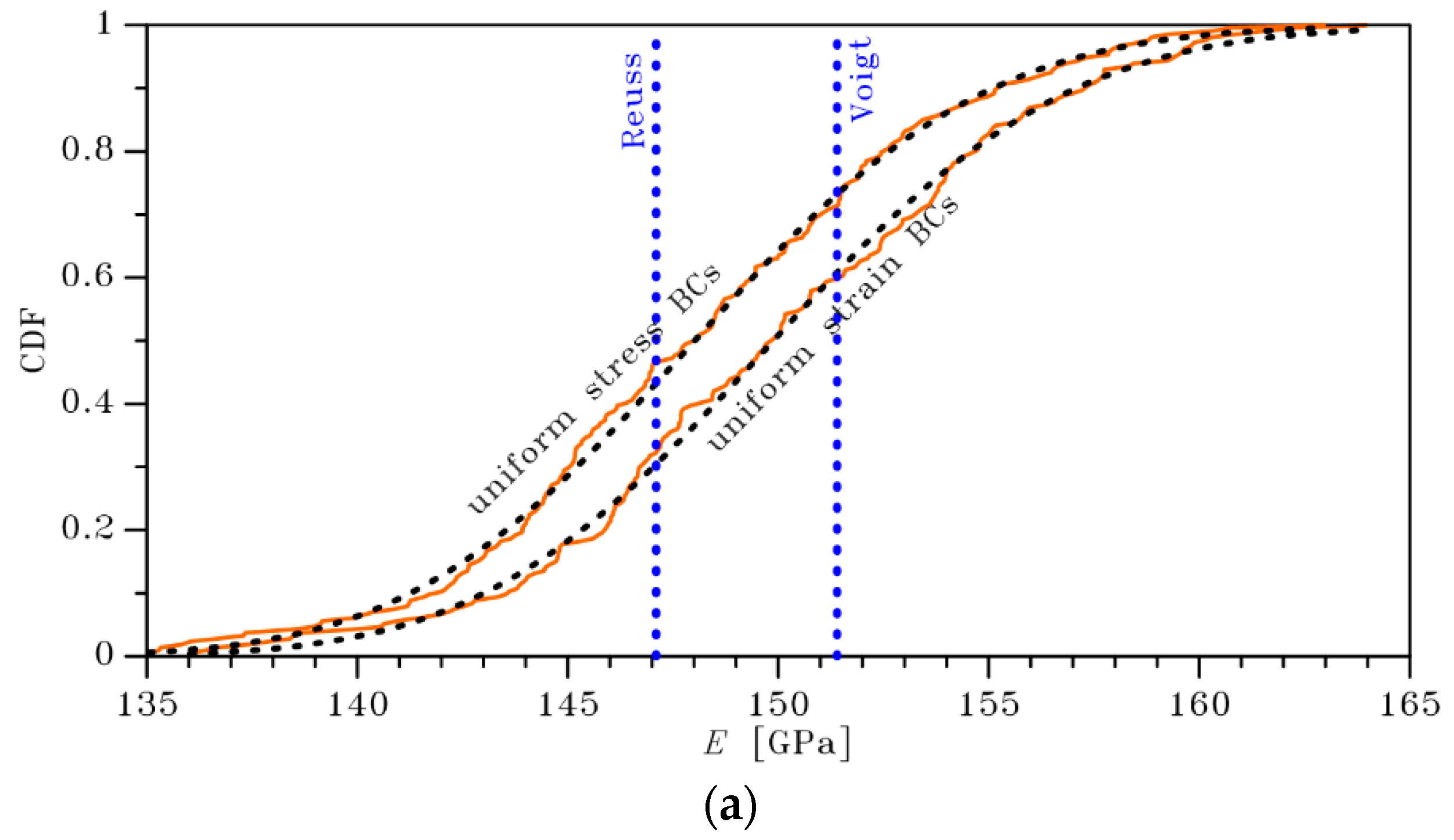
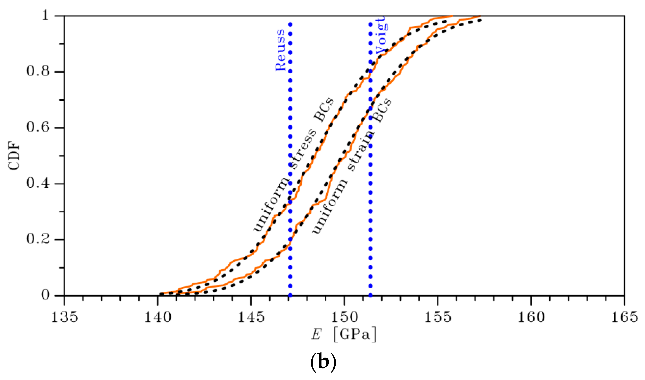
The cumulative distribution functions bounding , as obtained with the two types of BCs and for μm and μm, are shown in Figure 3 together with the relevant analytical lognormal interpolations. The lognormal distribution, whose details in the cases under consideration are reported in Table 1, has been selected in place of, e.g., a Gaussian or normal one, since it automatically satisfies the thermodynamic constraint for which must be positive. Accordingly, it is deterministically set that unphysical, negative values of the Young’s modulus of the film cannot be sampled from the distributions obtained. To provide a comparative assessment between the current bounds and the former deterministic ones given in Section 3.1, the vertical lines in Figure 3 provide such latter tight ones.
An interesting feature of the results is that the mean values of the computed distributions are very close to the average between the Reuss and Voigt bounds. What is instead majorly affected in the solution is the scattering of the values around the mean, and the dependence of the standard deviation on (see also [36]).
4. Monte Carlo Analysis: Sensitivity to Imperfections
Stochastic effects on the device sensitivity, which results to be proportional to the amplitude of the oscillations of the resonant structure, are now assessed. These effects play a role in defining confidence intervals for additional performance indices like, e.g., power consumption, bandwidth, and resolution, see [5,6,7]. The focus of this study is anyway on micro-scale imperfections, as measured by the scattering in the beam width and in the effective Young’s modulus of the polysilicon film around the target values.
Micro-structural effects on the value of have been already investigated in Section 3; micro-fabrication effects on are instead handled in terms of an over-etch depth . By means of purposely designed on-chip testing devices featuring very slender movable structures, we already quantified the impact of on the aforementioned scattering. In fact, changes the in-plane film width, whose value turns out to be while represents only a target size; accordingly, the cross-sectional area of the beam is affected linearly by , whereas the moment of inertia is affected cubically. The over-etch depth also has primary indirect effects on : the gap at the capacitors, if the depth is assumed to be isotropically distributed within the wafer plane, is given by , where again represents only a target value. The temperature raise at mid-span, given by:
where, besides the variables already introduced in Section 2, and respectively represent the polysilicon resistivity and thermal conductivity, is affected as well due to its dependence on the cross-sectional area .
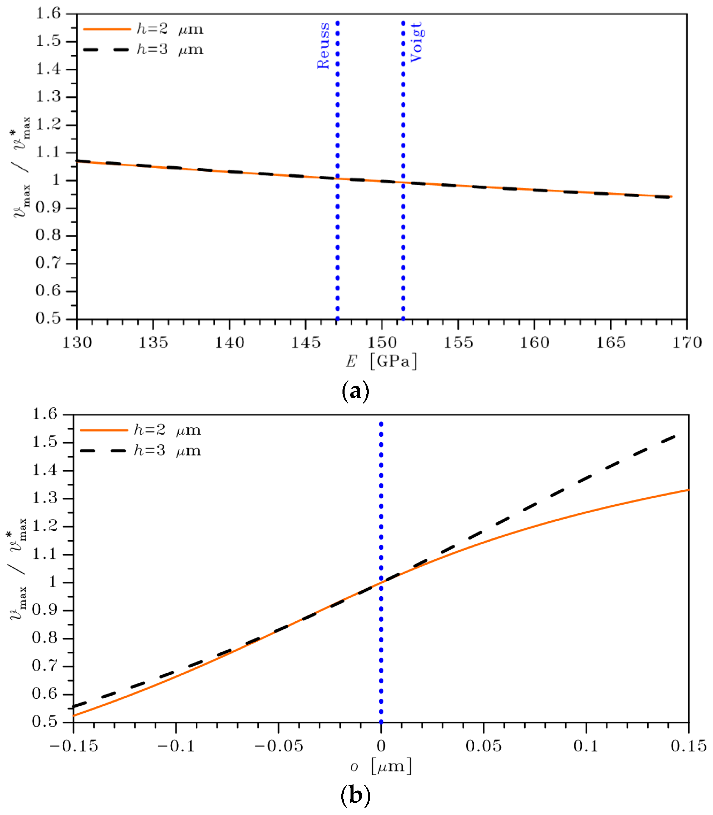
Before moving to the results of the Monte Carlo simulation, a sensitivity analysis is provided to assess the dependence of the dynamic response of the beam on and . In this analysis, the values of all the parameters have been set as gathered in Table 2, see also [5]. The value of the magnetic field intensity, with the aim discussed in [29] of developing devices for compass applications, has been assumed to be μT.
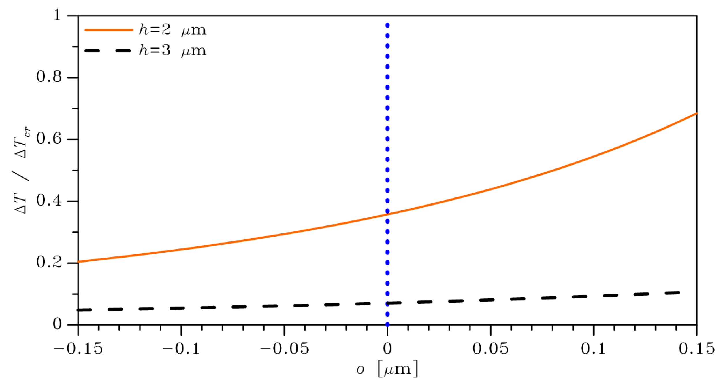
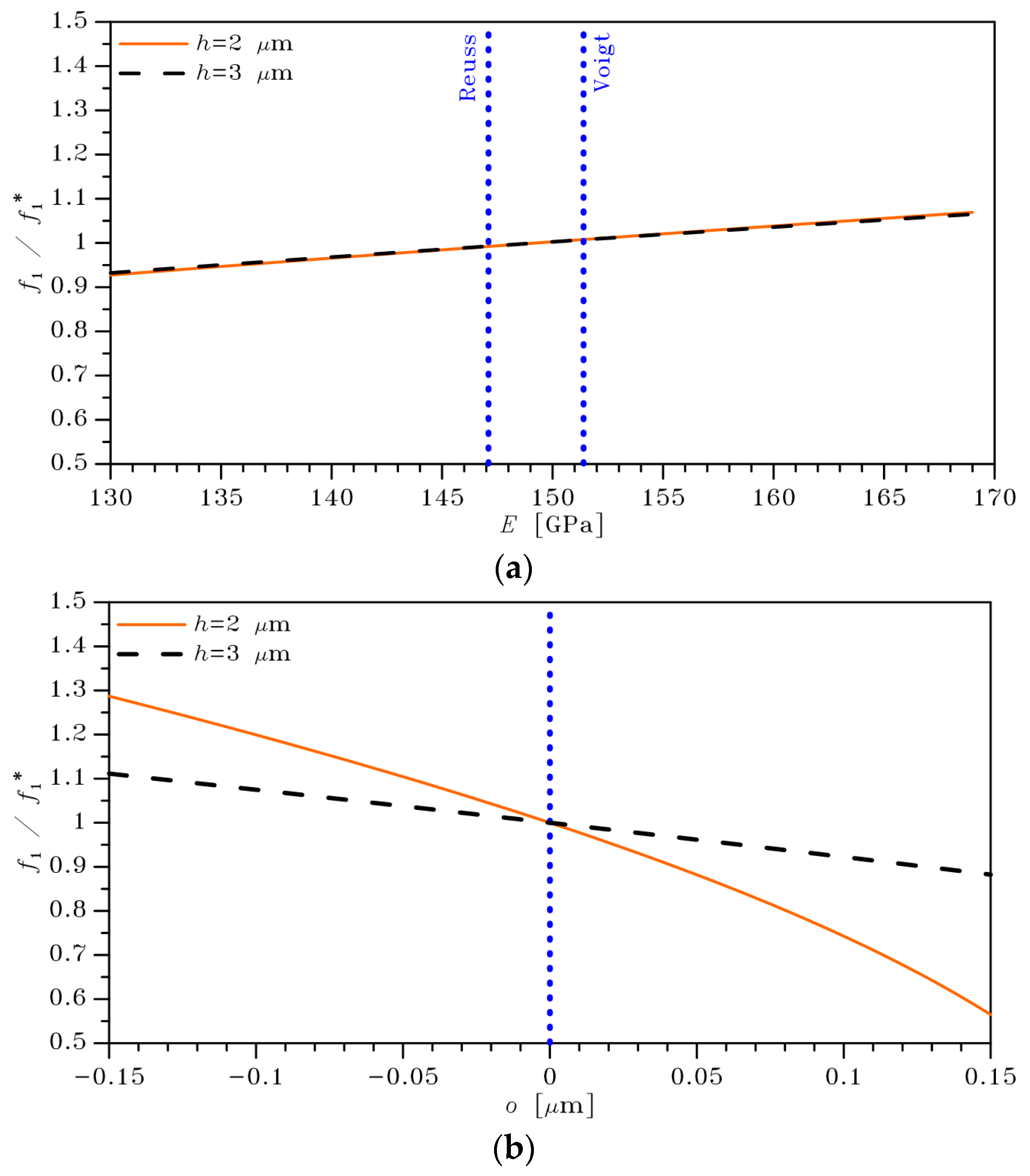
The impact of and on the response of the movable structure is shown in Figure 4, in terms of for both the target values of the beam thickness considered in the stochastic homogenization procedure of Section 3. In the plots, results are reported in a dimensionless form, to focus more on the trends at varying parameter values, rather than on the amplitude itself; for both the considered geometries, the amplitude of oscillations is therefore divided by a reference value linked to 149.25 GPa and . In the considered cases, this reference amplitude amounts to: 0.028 μm; 0.016 μm. The effect of the increased beam stiffness for is clear in these values; keeping aside such difference between the reference values, the dimensionless plots of Figure 4 allow to catch the trends in the system response. affects the linear stiffness and, therefore, the natural frequency at which is computed; the solution in terms of the oscillations amplitude accordingly turns out to be a weakly nonlinear function of the beam elastic properties, as shown in Figure 4a. The impact of on the solution is rather small; in order to report a variation still below 10% around the reference one, the range of values of the Young’s modulus has been extended to include all those possible for an ideal single-crystalline silicon sample, that is 130 GPa 169 GPa [40]. To better assess the smaller variability for a polycrystalline aggregate, independently of the target value of the film width, the analytical bounds and are also displayed with the vertical blue dotted lines. A much larger effect is due to the depth of the over-etch: Figure 4b shows that a variation of up to about 50% around can be attained in the range –0.15 μm 0.15 μm, as selected for the considered micro-fabrication process. Terms , , and are all affected by , and the solution thus shows the nonlinear dependence depicted in the graph, where the vertical blue dotted line is reported just to identify the condition of null leading to the reference value . In the adopted nondimensional format, the solution relevant to , though characterized by a smaller amplification for positive values, shows a remarkable nonlinearity induced by the Joule effect. This is reported also in Figure 5, where the mid-span temperature raise is plotted against the over-etch depth; once again, results are provided in a dimensionless form to better assess how close the actuation parameters and in Table 2 are to those leading to buckling. For this configuration, the critical value of the temperature raise is given by:
and, due to its dependence on and , it is affected by as well. A reduction of the film width, given by positive values of , leads to an increase of and a simultaneous decrease of , overall causing the nonlinear variation of shown in Figure 5 for both the target beam widths. The dependence is obviously more pronounced for , so that an increase of the excitation current might induce buckling by exceeding the threshold , especially in the stochastic environment to be considered next.
Additional results of the parametric analysis are reported in Figure 6, in terms of the variation of the fundamental resonance frequency of the beam due to and o. Results are obtained by dividing the frequency by the reference one linked to and , which amounts to: 15.5 kHz; 28.9 kHz. Alike the results of Figure 4, the solution is slightly affected by and varies in a highly nonlinear manner due to for . In this case, the reduction of for values approaching is another indicator of the frequency tuning provided by system nonlinearities, with a larger reduction being an indicator of the proximity to buckling instability. This condition has been purposely selected, to show next how all the nonlinear effects have a role in setting the scattering of in a stochastic environment.
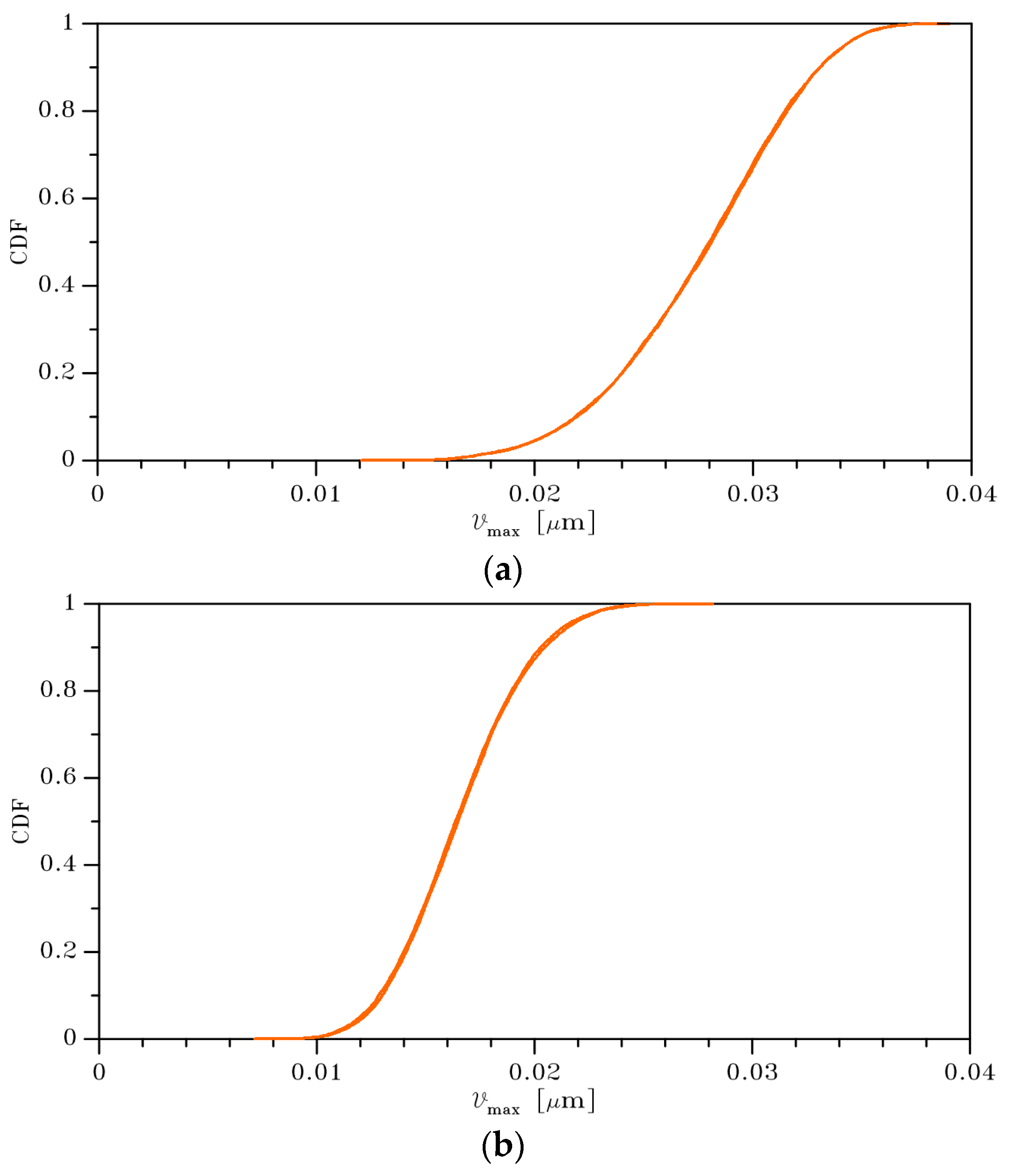
Results of the Monte Carlo analysis are now discussed. As far as is concerned, for each value of the lognormal distribution best fitting the results of the numerical homogenization of Section 3 has been adopted; we recall that, depending on the type of BCs, relevant values of mean and standard deviation are reported in Table 1. As for the over-etch, in accordance with former studies [15,16] its distribution has been assumed to be Gaussian, centered around the reference condition ; the corresponding standard deviation has been set to , so that the range −0.15 μm 0.15 μm inspected in the previous parametric analysis represents the 99.7% confidence interval.
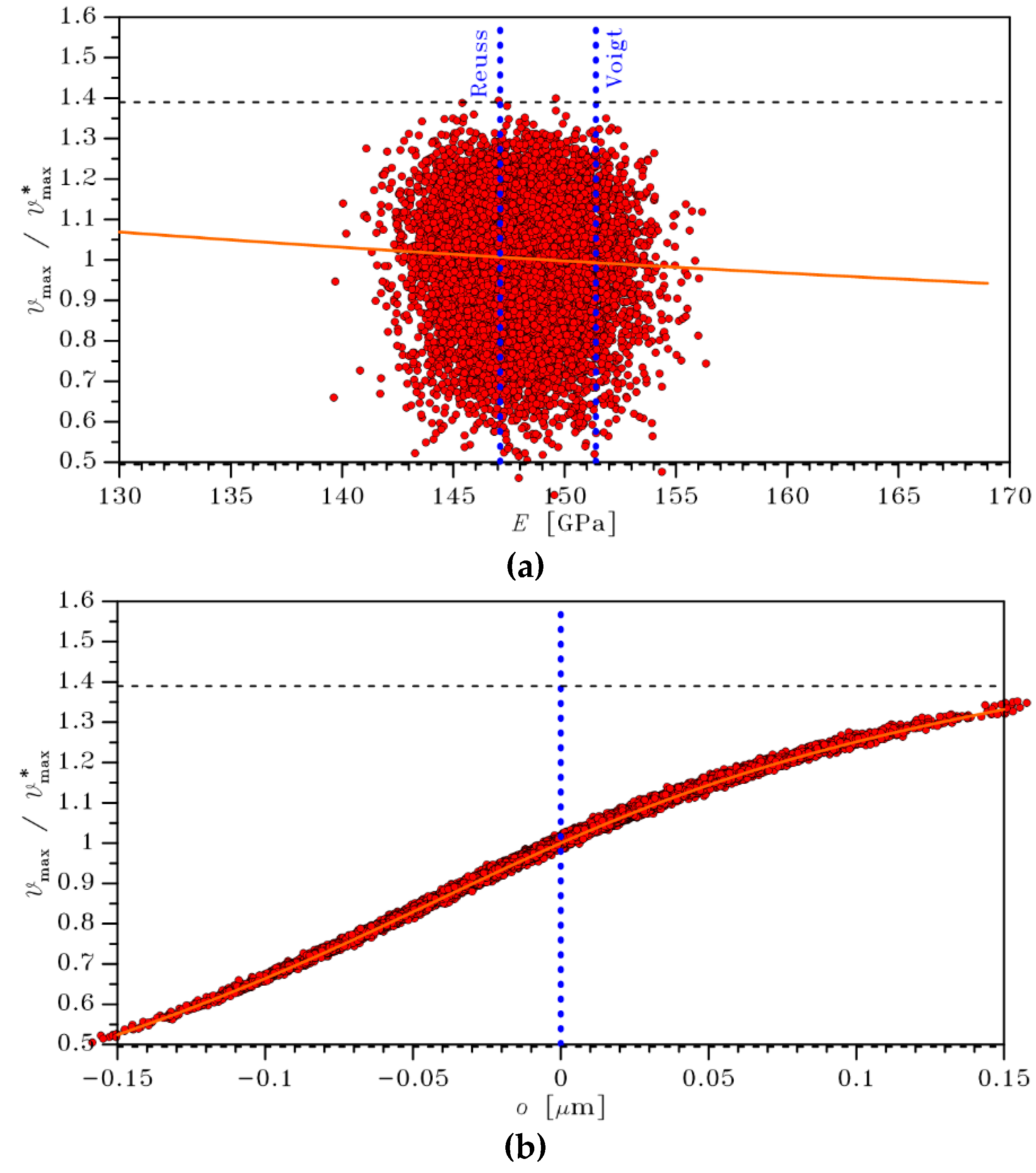
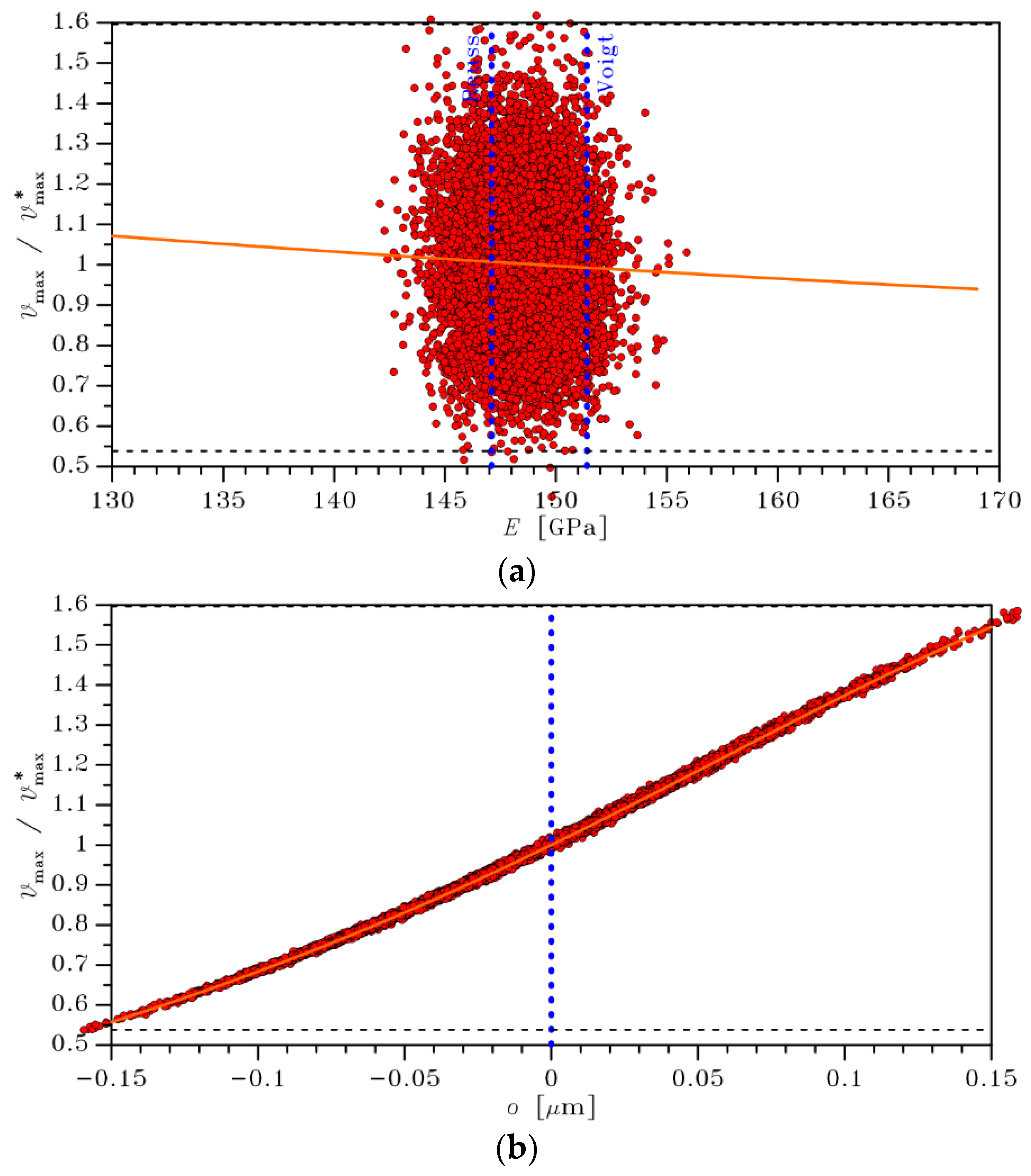
The output of the stochastic analysis is shown in Figure 7 and Figure 8 for and , respectively, in terms of the nondimensional values of . In these graphs, each dot represents a solution of the Monte Carlo simulation handling 10,000 samples. In the charts, the horizontal black dashed lines stand for the limits of the aforementioned confidence interval; the outliers falling outside such interval are clearly reported in the graphs versus , while they are partially dropped in the graphs versus to avoid widening too much the displayed interval beyond the previously discussed limits. The vertical blue dotted lines still represent the size-independent bounds and on the polysilicon Young’s modulus, and the reference no-over-etch case. The orange lines are, as in Figure 4, the trends provided by a varying at , and by a varying at . They are depicted to catch the relative importance of and on the scattering in the solution: while all the sampled outcome values lie close to the trend given by alone, they are much spread around the trend induced by . This is a clear qualitative measure of the higher importance of the role played by , as compared to that of .
To focus more on the quantitative analysis of the results, Figure 9 provides the cumulative distribution functions of for the two film widths considered. The relevant values of mean and standard deviation of , as affected by film width and type of BCs, are all collected in Table 3. As shown also by the graphs, the effect of the type of BCs is marginal: the curves relevant to uniform stress and uniform strain BCs can be hardly distinguished at the reported global scale. Once more, this is a proof of the much smaller impact of on the solution and, therefore, on the device performance, in comparison to that of .
To quantify next the sensitivity of the magnetometer, we refer to the differential sensing scheme provided by the two parallel plate capacitors depicted in Figure 1, see [4,7]. The magnitude of the capacitance change due to the deformation of the beam, or flexure is given by:
where represents variation of the gap at the capacitors, or the amplitude of the lateral oscillations of the beam. By driving the device at frequency , at which represents the said variation of the gap, and by normalizing the results with respect to the intensity of the external magnetic field to sense, the following measure of the mechanical sensitivity is arrived at:
In accordance with the model discussed in Section 2, in Equation (12) it has been assumed that the gap at capacitors is homogeneously varied all over their surfaces. Hence, the plates attached to the beam get displaced as rigid bodies and, due to the geometrical symmetry, tilting of the plates is disregarded. Moreover, even though Figure 1 shows that the in-plane length of the stators is smaller than the length of the beam, the two measures have been assumed the same; results can be anyway generalized since, according to Equation (12), is proportional to .
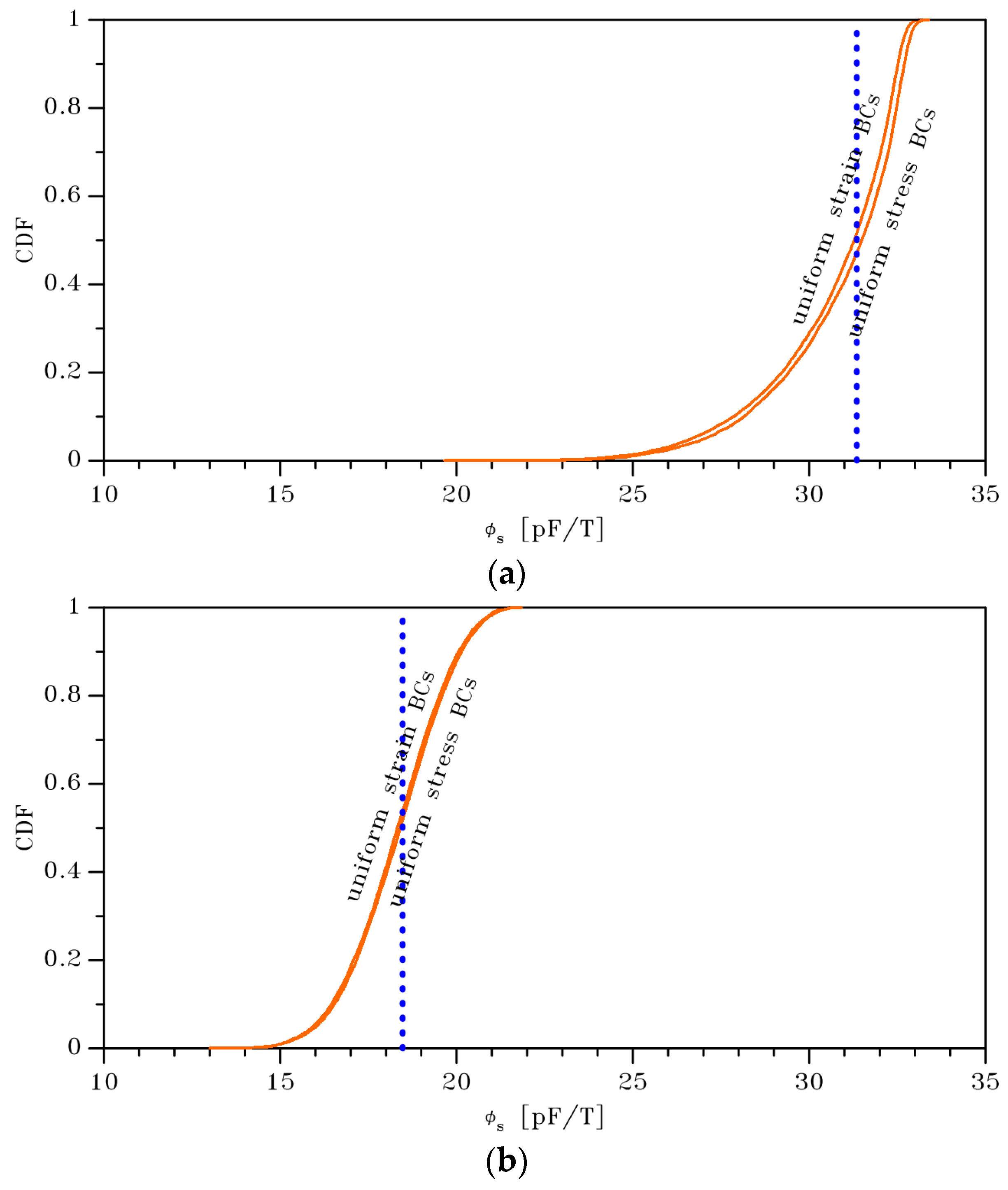
For the two target values of the beam width , reference values of turn out to be: 31.35 pF/T; 18.47 pF/T. The scattering in the sensitivity provided by the Monte Carlo analysis is shown in Figure 10, in terms of the cumulative distribution functions of . In these graphs, the vertical blue dotted lines represent the above mentioned -dependent reference values of the sensitivity. Statistics are also collected in Table 4, in terms of the values of mean and standard deviation of , depending on film width and type of BCs. The results testify that, due to the nonlinearities in the definition of the sensitivity and in the system response to the magnetic field, and to the scattering in the values of and , the cumulative distribution functions of the output result to be distorted in comparison with those relevant to the input parameters. Due to the compliance of the beam in the case, the curves relevant to the two types of BCs are not superposed, and can be distinguished at the scale of graph. At any rate, the plot clearly shows that, also for this performance index, the variation in the statistics linked to the BCs plays a marginal role, being largely superseded by the scattering induced by the two main parameters and handled in the Monte Carlo analysis.
5. Conclusions
In this work, we have discussed a single degree of freedom reduced-order model for the dynamics of the resonant structure of a single-axis Lorentz force MEMS magnetometer. By accounting for the (weakly) coupled thermo-electro-magneto-mechanical multi-physics governing the vibrations of the slender clamped-clamped resonant beam, its motion turned out to be described by the Duffing equation, where nonlinearities are enhanced by the end constraints on the motion itself.
Since the Joule effect, caused by the current flowing along the longitudinal axis of the beam, induces a temperature rise that may get close to values leading to buckling instability (while pull-in is avoided due to the small amplitude of the vibrations of the flexure), the characteristics of the structural vibrations turn out to be highly affected by micromechanical imperfection-like fluctuations of stiffness and geometry of the moving polysilicon film.
A statistical analysis has been developed, in order to assess the sensitivity of the sensor response to uncertainties in the values of the over-etch depth and of the morphology-driven overall Young’s modulus of the polycrystalline silicon. A Monte Carlo investigation has been carried out, wherein the over-etch depth has been sampled out of a micro-fabrication tailored normal distribution, and the Young’s modulus has been sampled out of a size-dependent lognormal distribution obtained by best fitting the outcomes of a stochastic homogenization on samples (or statistical volume elements) of the polycrystalline film.
A sensitivity analysis has shown that the amplitude of oscillations of the resonant beam of this Lorentz force MEMS magnetometer is marginally affected by the elasticity of polysilicon, while it strongly depends on the over-etch depth. Similar results have been arrived at with the Monte Carlo simulations, which have highlighted that the scattering in the beam response and in the mechanical sensitivity of the device basically follow the trend induced by the over-etch and, therefore, by its geometry rather than by its elastic properties.
In the present analysis some simplifying assumptions have been introduced, in order to obtain the handled single degree of freedom reduced-order model. First, as motivated in the end by the far different effects of elastic and geometrical features on the vibrations amplitude, the statistical distributions of Young’s modulus and over-etch depth have been assumed independent. This is clearly an approximation, as it has been remarked here above that the lognormal function describing the statistics of the polysilicon Young’s modulus is size-dependent and, therefore, etch-dependent. Second, it has been assumed that the polysilicon Young’s modulus and the over-etch depth do not vary along the beam axis, hence they are homogeneous in space. This is a further approximation since, in reality, the morphology of the film stochastically varies from point to point, and the over-etch depth is not uniform, even inside a single die. Third, the purposely developed reduced-order model has been based on one deformation mode for the structure, so that internal resonances and additional higher-order effects turned out to be all disregarded. Fourth, the values of the silicon parameters handled in the analysis have been assumed constant, though they can depend on the concentration of dopants like phosphorous and boron. All these effects are going to be taken into account in future developments of the present work.
Author Contributions
The authors contributed equally to this work.
Funding
Financial support provided by STMicroelectronics through project MaRe (Material Reliability) is gratefully acknowledged.
Acknowledgments
Authors are indebted to Roberto Martini, Aldo Ghisi, Ramin Mirzazadeh and Marco Geninazzi for the support in developing the codes and collecting the results related to stochastic homogenization.
Conflicts of Interest
The authors declare no conflict of interest.
References
- Gad-el-Hak, M. (Ed.) The MEMS Handbook; CRC Press: Boca Raton, FL, USA, 2002. [Google Scholar]
- Ko, W. Trends and frontiers of MEMS. Sens. Actuators A-Phys. 2007, 136, 62–67. [Google Scholar] [CrossRef]
- Corigliano, A.; Ardito, R.; Comi, C.; Frangi, A.; Ghisi, A.; Mariani, S. Mechanics of Microsystems; John Wiley and Sons: Hoboken, NJ, USA, 2018. [Google Scholar]
- Li, M.; Rouf, V.T.; Thompson, M.J.; Horsley, D.A. Three-axis Lorentz-force magnetic sensor for electronic compass applications. J. Microelectromech. Syst. 2012, 21, 1002–1010. [Google Scholar] [CrossRef]
- Bagherinia, M.; Bruggi, M.; Corigliano, A.; Mariani, S.; Lasalandra, E. Geometry optimization of a Lorentz force, resonating MEMS magnetometer. Microelectron. Reliabil. 2014, 54, 1192–1199. [Google Scholar] [CrossRef]
- Bagherinia, M.; Corigliano, A.; Mariani, S.; Horsley, D.A.; Li, M.; Lasalandra, E. An efficient earth magnetic field MEMS sensor: Modelling and experimental results. In Proceedings of the MEMS IEEE, San Francisco, CA, USA, 26–30 January 2014; pp. 700–703. [Google Scholar]
- Bagherinia, M.; Bruggi, M.; Corigliano, A.; Mariani, S.; Horsley, D.A.; Li, M.; Lasalandra, E. An efficient earth magnetic field MEMS sensor: Modeling, experimental results and optimization. J. Microelectromech. Syst. 2015, 24, 887–895. [Google Scholar] [CrossRef]
- Corigliano, A.; De Masi, B.; Frangi, A.; Comi, C.; Villa, A.; Marchi, M. Mechanical characterization of polysilicon through on-chip tensile tests. J. Microelectromech. Syst. 2004, 13, 200–219. [Google Scholar] [CrossRef]
- Mariani, S.; Ghisi, A.; Corigliano, A.; Zerbini, S. Multi-scale analysis of MEMS sensors subject to drop impacts. Sensors 2007, 7, 1817–1833. [Google Scholar] [CrossRef] [PubMed]
- Ghisi, A.; Fachin, F.; Mariani, S.; Zerbini, S. Multi-scale analysis of polysilicon MEMS sensors subject to accidental drops: Effect of packaging. Microelectron. Reliabil. 2009, 49, 340–349. [Google Scholar] [CrossRef]
- Ghisi, A.; Kalicinski, S.; Mariani, S.; De Wolf, I.; Corigliano, A. Polysilicon MEMS accelerometers exposed to shocks: Numerical-experimental investigation. J. Micromech. Microeng. 2009, 19, 035023. [Google Scholar] [CrossRef]
- Mariani, S.; Ghisi, A.; Corigliano, A.; Zerbini, S. Modeling impact-induced failure of polysilicon MEMS: A multi-scale approach. Sensors 2009, 9, 556–567. [Google Scholar] [CrossRef]
- Mariani, S.; Martini, R.; Ghisi, A.; Corigliano, A.; Simoni, B. Monte Carlo simulation of micro-cracking in polysilicon MEMS exposed to shocks. Int. J. Fract. 2011, 167, 83–101. [Google Scholar] [CrossRef]
- Mariani, S.; Martini, R.; Corigliano, A.; Beghi, M. Overall elastic domain of thin polysilicon films. Comput. Mater. Sci. 2011, 50, 2993–3004. [Google Scholar] [CrossRef]
- Mirzazadeh, R.; Eftekhar Azam, S.; Mariani, S. Micromechanical characterization of polysilicon films through on-chip tests. Sensors 2016, 16, 1191. [Google Scholar] [CrossRef] [PubMed]
- Mirzazadeh, R.; Mariani, S. Uncertainty quantification of microstructure-governed properties of polysilicon MEMS. Micromachines 2017, 8, 248. [Google Scholar] [CrossRef]
- Mirzazadeh, R.; Eftekhar Azam, S.; Mariani, S. Mechanical characterization of polysilicon MEMS: A hybrid TMCMC/POD-kriging approach. Sensors 2018, 18, 1243. [Google Scholar] [CrossRef]
- Mariani, S.; Ghisi, A.; Mirzazadeh, R.; Eftekhar Azam, S. On-Chip testing: A miniaturized lab to assess sub-micron uncertainties in polysilicon MEMS. Micro Nanosyst. 2018, 10, 84–93. [Google Scholar] [CrossRef]
- Bagherinia, M.; Mariani, S.; Corigliano, A.; Lasalandra, E. Stochastic effects on the dynamics of a resonant MEMS magnetometer: A Monte Carlo investigation. In Proceedings of the 1st International Electronic Conference on Sensors and Applications, Basel, Switzerland, 1–16 June 2014. [Google Scholar]
- Bahreyni, B.; Shafai, C. A micromachined magnetometer with frequency modulation at the output. In Proceedings of the MEMS IEEE 2005, Irvine, CA, USA, 30 October–3 November 2005; pp. 580–583. [Google Scholar]
- Bahreyni, B.; Shafai, C. A Resonant Micromachined Magnetic Field Sensor. IEEE Sens. J. 2007, 7, 1326–1334. [Google Scholar] [CrossRef]
- Ghosh, S.; Lee, J.E.-Y. A piezoelectric-on-silicon width-extensional mode Lorentz force resonant MEMS magnetometer. Sens. Actuators A Phys. 2017, 260, 169–177. [Google Scholar] [CrossRef]
- Ko, J.S.; Lee, M.L.; Lee, D.S.; Choi, C.A.; Kim, Y.T. Development and application of laterally driven electromagnetic microactuator. Appl. Phys. Lett. 2002, 81, 547–549. [Google Scholar]
- Kumar, V.; Mazrouei Sebdani, S.; Pourkamali, S. Sensitivity enhancement of a Lorentz force MEMS magnetometer with frequency modulated output. J. Microelectromech. Syst. 2017, 26, 870–878. [Google Scholar] [CrossRef]
- Wu, L.; Tian, Z.; Ren, D.; You, Z. A Miniature resonant and torsional magnetometer based on Lorentz force. Micromachines 2018, 9, 666. [Google Scholar] [CrossRef]
- Aydemir, G.A.; Saranlı, A. Characterization and calibration of MEMS inertial sensors for state and parameter estimation applications. Measurement 2012, 45, 1210–1225. [Google Scholar] [CrossRef]
- Camps, F.; Harasse, S.; Monin, A. Numerical calibration for 3-axis accelerometers and magnetometers. In Proceedings of the IEEE International Conference on Electro/Information Technology, Windsor, ON, Canada, 7–9 June 2009; pp. 217–221. [Google Scholar]
- LSM6DSOX Datasheet; Technical Report; STMicroelectronics: Geneva, Switzerland, 2019.
- Bagherinia, M. MEMS Sensors for Measuring the Earth Magnetic Field: Mechanical Aspects. Ph.D. Thesis, Politecnico di Milano, Milan, Italy, 2014. [Google Scholar]
- Younis, M.I. MEMS Linear and Nonlinear Statics and Dynamics; Springer: New York, NY, USA, 2011. [Google Scholar]
- Shih, Y.S.; Wu, G.Y.; Chen, E.J.S. Transient vibrations of a simply-supported beam with axial loads and transverse magnetic fields. Mech. Struct. Mech. 1998, 26, 115–130. [Google Scholar] [CrossRef]
- Xi, X.; Yang, Z.; Meng, L.; Zhu, C. Primary resonance of the current-carrying beam in thermal-magneto-elasticity field. Appl. Mech. Mater. 2010, 29–32, 16–21. [Google Scholar] [CrossRef]
- Comi, C.; Corigliano, A.; Langfelder, G.; Longoni, A.; Tocchio, A.; Simoni, B. A resonant microaccelerometer with high sensitivity operating in an oscillating circuit. J. Microelectromech. Syst. 2010, 19, 1140–1152. [Google Scholar] [CrossRef]
- Han, J.S.; Ko, J.S.; Korvink, J.G. Structural optimization of a large-displacement electromagnetic Lorentz force microactuator for optical switching applications. J. Micromech. Microeng. 2004, 14, 1585–1596. [Google Scholar] [CrossRef]
- Bao, M.; Yang, H. Squeeze film air damping in MEMS. Sens. Actuators A 2007, 136, 3–27. [Google Scholar] [CrossRef]
- Mariani, S.; Martini, R.; Ghisi, A.; Corigliano, A.; Beghi, M. Overall elastic properties of polysilicon films: A statistical investigation of the effects of polycrystal morphology. Int. J. Multiscale Comput. Eng. 2011, 9, 327–346. [Google Scholar] [CrossRef]
- Nemat-Nasser, S.; Hori, M. Micromechanics: Overall Properties of Heterogeneous Materials; Volume 37 of Applied Mathematics and Mechanics; North-Holland: Amsterdam, The Netherlands, 1993. [Google Scholar]
- Cho, S.; Chasiotis, I. Elastic properties and representative volume element of polycrystalline silicon for MEMS. Exp. Mech. 2007, 47, 37–49. [Google Scholar] [CrossRef]
- Sanchez-Palencia, E. Nonhomogeneous Media and Vibration Theory; Volume 127 of Lecture Notes in Physics; Springer: Berlin Heidelberg, Germany, 1980. [Google Scholar]
- Hopcroft, M.A.; Nix, W.D.; Kenny, T.W. What is the Young’s Modulus of Silicon? J. Microelectromech. Syst. 2010, 19, 229–238. [Google Scholar] [CrossRef]
- McConnell, A.D.; Uma, S. Thermal conductivity of doped polysilicon layers. J. Microelectromech. Syst. 2001, 10, 360–369. [Google Scholar] [CrossRef]
Figure 1.
(a) SEM picture of a movable structure of the resonant MEMS magnetometer [19], and (b) scheme of the structure with the notation adopted.
Figure 1.
(a) SEM picture of a movable structure of the resonant MEMS magnetometer [19], and (b) scheme of the structure with the notation adopted.

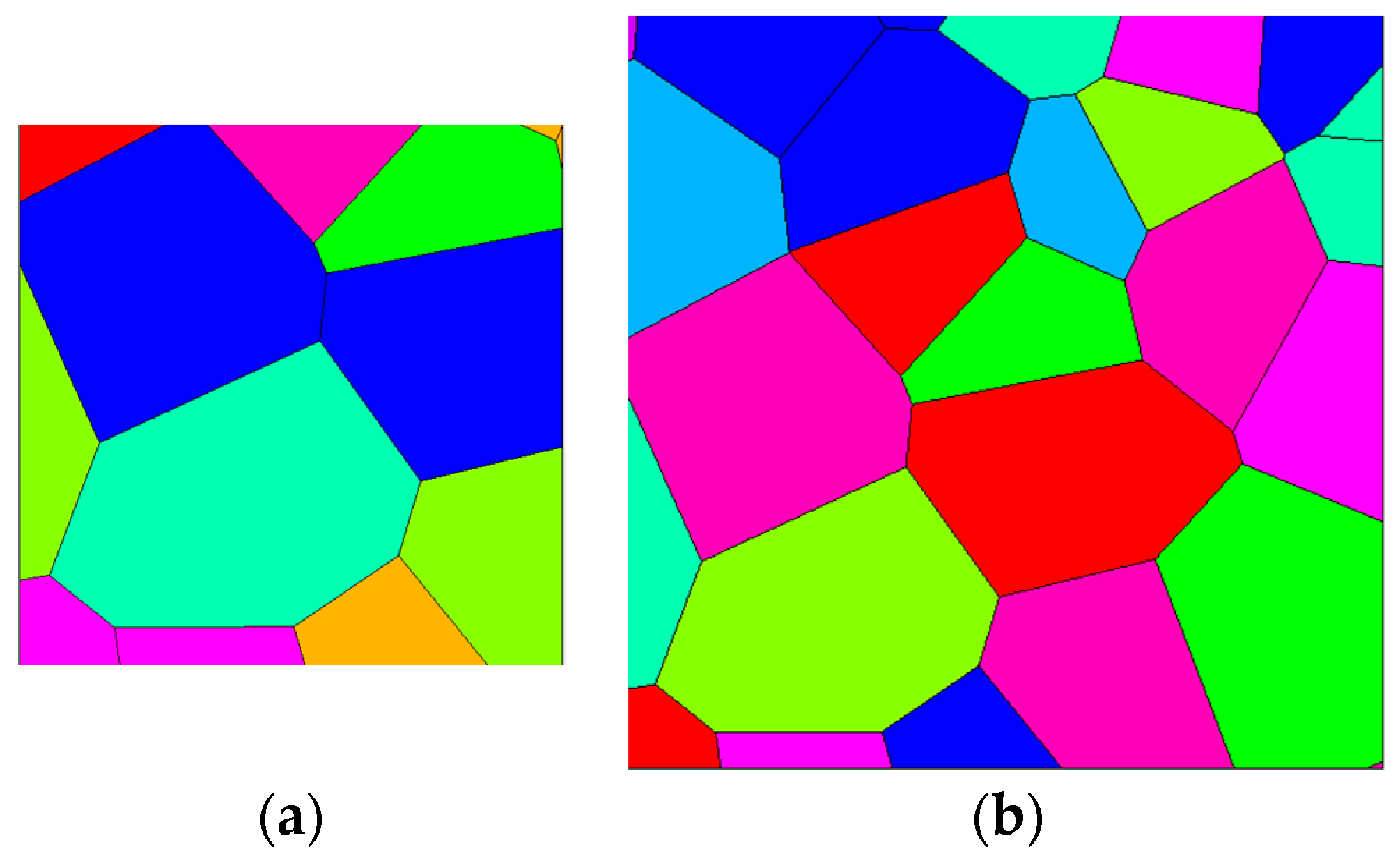
Figure 2.
Exemplary regularized micro-structures of (a) 2 × 2 μm and (b) 3 × 3 μm SVEs, where grains are depicted with different colors.
Figure 2.
Exemplary regularized micro-structures of (a) 2 × 2 μm and (b) 3 × 3 μm SVEs, where grains are depicted with different colors.

Figure 3.
Stochastic homogenization, effect of the SVE size on the cumulative distribution functions of the bounds on the homogenized in-plane Young’s modulus of a polysilicon film featuring μm: (a) 2 ×2 μm SVE, (b) 3 × 3 μm SVE.
Figure 3.
Stochastic homogenization, effect of the SVE size on the cumulative distribution functions of the bounds on the homogenized in-plane Young’s modulus of a polysilicon film featuring μm: (a) 2 ×2 μm SVE, (b) 3 × 3 μm SVE.


Figure 4.
Sensitivity analysis: dependence of (a) on the polysilicon effective Young’s modulus , and (b) on the over-etch depth .
Figure 4.
Sensitivity analysis: dependence of (a) on the polysilicon effective Young’s modulus , and (b) on the over-etch depth .

Figure 5.
Sensitivity analysis: dependence on the over-etch depth of the ratio between the temperature raise at mid-span, as induced by Joule effect, and its critical value .
Figure 5.
Sensitivity analysis: dependence on the over-etch depth of the ratio between the temperature raise at mid-span, as induced by Joule effect, and its critical value .

Figure 6.
Sensitivity analysis: dependence of the natural frequency (a) on the polysilicon effective Young’s modulus , and (b) on the over-etch depth .
Figure 6.
Sensitivity analysis: dependence of the natural frequency (a) on the polysilicon effective Young’s modulus , and (b) on the over-etch depth .

Figure 7.
Monte Carlo simulation, μm: scattering in the value of , and comparison with the trends induced by (a) and (b) alone.
Figure 7.
Monte Carlo simulation, μm: scattering in the value of , and comparison with the trends induced by (a) and (b) alone.

Figure 8.
Monte Carlo simulation, μm: scattering in the value of , and comparison with the trends induced by (a) and (b) alone.
Figure 8.
Monte Carlo simulation, μm: scattering in the value of , and comparison with the trends induced by (a) and (b) alone.

Figure 9.
Monte Carlo simulation: cumulative distribution functions of for (a) μm and (b) μm.

Figure 10.
Monte Carlo simulation: cumulative distribution functions of the sensitivity for (a) μm and (b) μm.
Figure 10.
Monte Carlo simulation: cumulative distribution functions of the sensitivity for (a) μm and (b) μm.


Table 1.
Stochastic homogenization: effect of the SVE size on the mean and standard deviation of the scattered in-plane polysilicon Young’s modulus.
Table 1.
Stochastic homogenization: effect of the SVE size on the mean and standard deviation of the scattered in-plane polysilicon Young’s modulus.
| SVE Size | Uniform Stress BCs | Uniform Strain BCs | ||
|---|---|---|---|---|
| (GPa) | (GPa) | (GPa) | (GPa) | |
| 2 × 2 μm2 | 148.1 | 5.4 | 150.0 | 5.5 |
| 3 × 3 μm2 | 148.4 | 3.3 | 149.9 | 3.3 |
Table 2.
Values of the geometrical, physical, actuation, and sensing parameters adopted in the analysis.
Table 2.
Values of the geometrical, physical, actuation, and sensing parameters adopted in the analysis.
| Property | Value |
|---|---|
| beam length (μm) | |
| beam width (μm) | |
| beam thickness (μm) | |
| gap (μm) | |
| mass density (kg/m3), [40] | |
| thermal expansion coefficient (K−1), [40] | |
| thermal conductivity (W/mK), [41] | |
| resistivity (Ωm), [41] | |
| permittivity (F/m) | |
| air viscosity (Ns/m2), [35] | |
| actuation current (mA) | |
| bias voltage (V) | |
| magnetic field intensity (μT), [4] |
Table 3.
Monte Carlo simulation: effect of the target in-plane film width and of the type of BCs on the values of mean and standard deviation of the scattered amplitude of oscillations.
Table 3.
Monte Carlo simulation: effect of the target in-plane film width and of the type of BCs on the values of mean and standard deviation of the scattered amplitude of oscillations.
| Uniform Stress BCs | Uniform Strain BCs | |||
|---|---|---|---|---|
| (μm) | (μm) | (μm) | (μm) | (μm) |
| 2 | 0.028 | 0.004 | 0.028 | 0.004 |
| 3 | 0.017 | 0.003 | 0.016 | 0.003 |
Table 4.
Monte Carlo simulation: effect of the target in-plane film width and of the type of BCs on the values of mean and standard deviation of the scattered device sensitivity.
Table 4.
Monte Carlo simulation: effect of the target in-plane film width and of the type of BCs on the values of mean and standard deviation of the scattered device sensitivity.
| Uniform Stress BCs | Uniform Strain BCs | |||
|---|---|---|---|---|
| (μm) | (pF/T) | (pF/T) | (pF/T) | (pF/T) |
| 2 | 30.89 | 1.90 | 30.67 | 1.93 |
| 3 | 18.36 | 1.38 | 18.28 | 1.38 |
© 2019 by the authors. Licensee MDPI, Basel, Switzerland. This article is an open access article distributed under the terms and conditions of the Creative Commons Attribution (CC BY) license (http://creativecommons.org/licenses/by/4.0/).
Share and Cite
MDPI and ACS Style
Bagherinia, M.; Mariani, S. Stochastic Effects on the Dynamics of the Resonant Structure of a Lorentz Force MEMS Magnetometer. Actuators 2019, 8, 36. https://doi.org/10.3390/act8020036
AMA Style
Bagherinia M, Mariani S. Stochastic Effects on the Dynamics of the Resonant Structure of a Lorentz Force MEMS Magnetometer. Actuators. 2019; 8(2):36. https://doi.org/10.3390/act8020036
Chicago/Turabian StyleBagherinia, Mehrdad, and Stefano Mariani. 2019. "Stochastic Effects on the Dynamics of the Resonant Structure of a Lorentz Force MEMS Magnetometer" Actuators 8, no. 2: 36. https://doi.org/10.3390/act8020036
Note that from the first issue of 2016, this journal uses article numbers instead of page numbers. See further details here.