Article

Photoconduction of Polar and Nonpolar Cuts of Undoped Sr0.61Ba0.39Nb2O6 Single Crystals

1
Institute of Applied Physics, Technische Universität Dresden, 01062 Dresden, Germany
2
Prokhorov Institute of General Physics, Russian Academy of Sciences, 119991 Moscow, Russia
3
ct.qmat: Dresden-Würzburg Cluster of Excellence—EXC 2147, TU Dresden, 01062 Dresden, Germany
*
Author to whom correspondence should be addressed.
Crystals 2021, 11(7), 780; https://doi.org/10.3390/cryst11070780
Submission received: 24 May 2021 / Revised: 28 June 2021 / Accepted: 1 July 2021 / Published: 3 July 2021
(This article belongs to the Special Issue Electrocrystallization of Metallic Alloys and Composites)

Abstract

:
In the last two decades, variably doped strontium barium niobate (SBN) has attracted a lot of scientific interest mainly due to its specific non-linear optical response. Comparably, the parental compound, i.e., undoped SBN, appears to be less studied so far. Here, two different cuts of single-crystalline nominally pure strontium barium niobate in the composition Sr0.61Ba0.39Nb2O6 (SBN61) are comprehensively studied and analyzed with regard to their photoconductive responses. We present conductance measurements under systematically varied illumination conditions along either the polar z-axis or perpendicular to it (x-cut). Apart from a pronounced photoconductance (PC) already under daylight and a large effect upon super-bandgap illumination in general, we observe (i) distinct spectral features when sweeping the excitation wavelength over the sub-bandgap region as then discussed in the context of deep and shallow trap states, (ii) extremely slow long-term relaxation for both light-on and light-off transients in the range of hours and days, (iii) a critical dependence of the photoresponse on the pre-illumination history of the sample, and (iv) a current–voltage hysteresis depending on both the illumination and the electrical-measurement conditions in a complex manner.

1. Introduction

The solid solution strontium barium niobate (Sr1−xBaxNb2O6, SBN) constitutes a fascinating material system, exhibiting a plethora of functional properties. These are highly sensitive to a number of internal (exact chemical composition, i.e., the value of x; doping by rare earth and/or transition metal ions [1], variation of oxygen content [2]) and external (electric, photonic, strain fields) stimuli and thus being effectively tunable for potential applications. In fact, the compound, which crystallizes in the tetragonal tungsten bronze (TTB) structure for 0.25 < x < 0.8 [3], has attracted a great deal of interest of different scientific communities within physics, chemistry, and materials research.
First of all, huge effort has been dedicated to exploring, optimizing, and exploiting the nonlinear optical, electrooptic, and photorefractive properties, which form the basis for applications such as holographic data storage or electro-optic modulation. In this context, mainly the congruently melting composition Sr0.61Ba0.39Nb2O6 (SBN61) doped with some selected ions such as cerium or chromium for enhancing the photorefractive response, and–to some lesser extent–the composition Sr0.75Ba0.25Nb2O6 (SBN75), exhibiting a maximum linear electro-optic coefficient r 33 , have been in the focus.
Second, in a certain composition range, SBN shows ferroelectric behavior; to be more precise, it belongs to the class of relaxor ferroelectrics that itself is interesting from a fundamental thermodynamical point of view [4], i.e., it shows broad ferroelectric–paraelectric transition ranges instead of a clear well-defined Curie temperature. Nanotechnological attempts such as domain wall and domain engineering appeared to be much more challenging than for standard ferroelectrics with respect to achieving reproducible and longterm stable structures, though there has been some significant success in recent years [5,6,7,8,9].
In the present study, we focus on the pronounced photoconduction of undoped SBN single crystals, which shows effects already under diffuse daylight (cf. Figure S1) and which has an impact on a number of SBN’s functional properties. In the past, the phenomenon has been investigated from at least three different points of view: (i) In the context of optimizing and understanding the photorefractive effect, photoconductive properties have been experimentally investigated in detail for Ce- and Cr-doped SBN [10,11,12,13], aiming at deriving the best-fitting deep-level center model for explaining the photoinduced charge transfer and on the quantitative extraction of charge transport parameters that were later employed for the theoretical modelling of the two-center holographic process [14]. (ii) Independently, triggered by the viewpoint of relaxor-ferroelectric behavior, the polarization kinetics of La-Ce co-doped SBN crystals [15,16,17,18,19] was compared for dark and white-light-illumination conditions and a decisive photoinduced tunability of the respective hysteresis loops was found. (iii) Apart from these quite fundamental works, there have been some selective recent activities in using the photovoltaic and photocatalytic properties of ceramic SBN [20,21]. As another example, even more on the road towards nanotechnological applications, SBN was successfully employed as a photochemical substrate for nanoparticle growth [22].
However, there seems to be a lack in the body of data concerning the undoped crystalline parent compound SBN61. The present study aims at bridging this gap, comprising photoconduction measurements in polar and unpolar cuts of SBN61 as a function of:
  • Wavelength in the range between 750 and 350 nm (i.e., 1.65–3.54 eV) revealing and discussing distinct spectral features being present already without distinct doping ions;
  • Time in order to describe the (pronounced long-term) relaxation behavior, which suggests special care in incorporating the material in nanoelectronic device concepts on the one hand and in interpreting optical-spectroscopy data results of any kind on the other hand;
  • Intensity for selected wavelength in order to link the results to known literature values recorded for doped SBN crystals;
  • Measuring voltage, which allows us to evaluate the current–voltage hysteresis behavior and extracting of the coercive voltage(s).

2. Materials and Methods

2.1. Crystal Growth

In the past, a number of different growth techniques have been employed to fabricate single-crystalline SBN, in most cases either by the Czochalski techniqe or the modified Stepanov technique. The latter can deliver crystals widely free of striation, cracks, extraneous phase inclusions, or bubbles and of high optical quality (variation of refractive index per cm crystal length: Δn = 1–2 × 10⁻⁵ cm−1). For the present study, a nominally pure, i.e., undoped, SBN crystal was grown by the aforementioned modified Stepanov technique, which has been described earlier [23,24,25]. All starting materials were of 4 N or better purity. The SBN crystal was grown along the tetragonal (polar) z-axis without rotation except for seeding and enlargement processes and the pulling rate was varied from 1 to 6 mm/h depending on the chemical composition of the melt. The optimal bulk crystallization rate was 2.5 cm3/h.
The SBN crystal was obtained in bulk-profiled configuration. Typical dimensions of the as-grown crystal were 70 mm long and 15 × 24 mm2 in cross section. Sample plates of 10 × 10 × 0.5 mm3 with orientation along and perpendicular to the z-axis were cut and polished from the as-grown polydomain SBN61 crystal to optical quality. In the following, we refer to them as x-cut and z-cut samples. The crystal growth process protocol has been verified within the framework of several previous investigations by X-ray (powder and microcrystal) diffraction [26,27] as well as neutron diffraction [28]. There, the single-crystal nature was proven and a refined quantitative analysis of different structural and compositional parameters could be established. As an additional integrity test of the two samples of the present study, the ferroelectric domain properties of the z-cut crystal plate were checked by piezoresponse force microscopy (PFM), revealing the typical fractal-like nanodomain pattern known from the literature [5,29], see Figure S2. Furthermore, extended domains written by an atomic-force-microscope tip were imaged via Cherenkov second-harmonic-generation microscopy (CSHG) to observe the vanishing of the domain contrast upon heating (Figure S3). This way the ferroelectric–paraelectric transition temperature range was found to be between 70 and 90 °C, again as expected from the literature, e.g., ref. [30].

2.2. Photoexcitation and Electrical-Measurement Configuration

Prior to any photoconduction experiments, the optical transmittance of the samples was recorded using a Shimadzu UV-3100PC spectrophotometer in order to extract and specify the bandgap.
For all subsequent phototransport measurements we used an illumination setup based on a 1000-Watt Xenon arc lamp (Oriel Instruments) as (white-)light source. The hot spot of its light arc is focused on the entrance slit of a grating monochromator (Cornerstone 260, Oriel Instruments) by a pair of fused-silica lenses. The light exiting the monochromator, which exhibits a spectral bandwidth of appromimately 10 nm, passes an appropriate edge filter (see Table 1) and a second pair of fused-silica lenses that produce a focus into which a fused-silica beam splitter is inserted, reflecting 10% of the incident power onto a power meter (Thorlabs PM100). A software feedback loop controls and varies the position of a motorized linear translation stage (Edmund Optics) that carries a variable neutral density filter (Thorlabs NDL-25C-4) to keep the photon flux constant across the whole spectrum.
The unpolarized light spot is imaged onto the sample surface by a third pair of lenses, with the sample fixed on a sapphire slide sitting on the sample holder of an exchange-gas liquid-nitrogen optical cryostat (Optistat DN by Oxford Instruments). Though all electrical measurements presented here, under illumination as well as in the dark, were conducted at room temperature (296 K), the cryostat served as (i) an efficient Faraday cage, and (ii) its sample space was filled with Helium gas to guarantee an inert atmosphere minimizing leakage currents by air humidity or by sparks when applying higher measuring voltages. Metallic contacts were painted by conductive silver paste. The rear side of the crystal was fully covered with the silver paste, which also served to glue the sample to the holder, while at the (illuminated) front side a 1 mm diameter silver dot was applied (see schematics in Figure 1). Thus, the current spread within the sample is expected to be cone-like. The distance between the contacted sides was 0.5 mm (equal to the thickness of the crystal plates). The resistance was obtained from measuring the current by a Keithley 6517B electrometer with active voltage source in two-point geometry using coaxial wiring down to the sample. For recording the wavelength dependence, the temporal relaxation, and the intensity dependence of the resistance the voltage source was set to 10 V, while for acquiring the I-V hysteresis the voltage was swept between up to ±300 V. Note that, as the silver paste used for the contacts is opaque, we do not expect the contact resistance to change under illumination. Typically, almost the whole sample surface (5 × 10 mm2) was illuminated. For dark-current measurements, the entrance window of the cryostat was completely shadowed by black tape.
For acquiring the wavelength dependence of the photoconductance in the range between 750 and 350 nm at a constant photon flux of 1.25 × 10¹⁴ s−1, the data was recorded in three, partially overlapping, runs (for technical and resolution reasons), starting always at the highest wavelength due to the long photorelaxation time of the material (for details see Table 1). Each partial spectrum was measured at least three times to check for sufficient reproducibility. The wavelength was varied in 1 nm steps and the respective resistance value was recorded after a waiting/settling time of one minute after adjusting a new wavelength point.
The most extensive part of this study, the recording of photoconductance transients upon on-/off-switching of the illumination at selected wavelengths (i.e., 800, 700, 600, 500, 450, 420, 400, 390, 380, 370, 360, and 350 nm), was performed as follows: The sample was kept in darkness for at least 20 h and its resistance was then measured for 10 min registering one data point every 2 s to calculate an average value R 0 . Subsequently, the illumination path was unblocked and the sample excited for 60 min to record the temporal evolution of the photoconductance, while, after blocking the beam path again, the relaxation of the resistance in darkness was monitored for 20 min. In the following, the time-dependent development of the resistance/conductance and any derived normalized quantity under illumination is referred to as light-on (photoconductance) transient, and the respective function after beam path blocking as light-off (photoconductance) transient. As will be explicitly discussed later, the values of the dark resistance R 0 (and its reciprocal counterpart, the dark conductance G 0 = 1 / R 0 ) vary in a certain range, depending on the pre-illumination history. Thus—for better comparability of the transients at the respective wavelengths—a normalized photoconductance value P C n o r m is employed, which is defined as follows:
P C n o r m : = G G 0 G 0 = G G 0 1 = R 0 R R = R 0 R 1 .
Here, R is the effectively measured resistance value reflecting the photoinduced excess carriers under illumination and also during the recovery process in the dark (with G = 1 / R being the respective conductance). Since a normalization according to Equation (1) makes the light-on transients effectively comparable, but gives less intuitive results for the light-off transients, for the latter a different normalization, being described f.i. in ref. [32], focusing on the residual excess level REL, is chosen:
R E L : = P C n o r m P C n o r m m a x = G G 0 G m a x G 0 ,
with P C n o r m m a x and G m a x here being the values for P C n o r m and the conductance G after the 60 min illumination period, respectively. Practically, the R E L value gives the fraction of the photoinduced maximal excess conductance that is still present after a given recovery period.
Apart from the 10 min dark/60 min illumination/20 min dark scheme, exemplary “ultra-longterm” transients were recorded for 370 nm illumination. At this wavelength, an extended illumination period of 200 min was applied, whereas the recovery of the resistance was monitored for 42 h in the dark, in order to get a clearer view on the very large relaxation times after super-bandgap illumination.
The intensity dependence of the photoconductivity reported for differently doped SBN crystals typically follows an empirical (sub-)linear relation [12,13]:
σ I x ,
with σ being the (photo-)conductivity, I the intensity, and x the fitting parameter lying typically in the range between 0.5 and 1 in the above cited studies. Here, we checked for the validity of this empirical law in the z-cut sample for sub- (500 nm) and super-bandgap (380 nm) illumination. For that purpose, the intensity was varied between 0.15 and 4.7 × 10⁻³ W/cm2, sweeping from low to high intensity. At every single intensity value (out of 13 measurement points in total) and after a settling time of 1 min, the resistance was recorded 20 times in 30 s intervals. Subsequently, an average value was calculated for the plot that served as the basis for the sublinear fit, but has to be seen as a compromise because of the ongoing slow photorelaxation of the crystals.
The investigation of the current–voltage characteristics was accomplished within different measurement scenarios. First, to check for ohmic or rectifying characteristics in the dark, the current was acquired while the measuring voltage was ramped in 5 V steps from 0 V to +100 V, then to −100 V, and finally back to 0 V, with waiting periods of 1 min after each voltage step. Second, while keeping the 5 V steps, we broadened the voltage range to ±300 V, in order to monitor also the ferroelectric switching process. Now, the current was recorded three times and averaged at each voltage setpoint. The retention time for each data point was 20 s with equally large time steps for collecting the three “raw” current values. The ±300 V scenario was performed not only in the dark but also under 500 nm and 380 nm illumination at a photon flux of 6.8 × 10¹⁵ s−1.

3. Results and Discussion

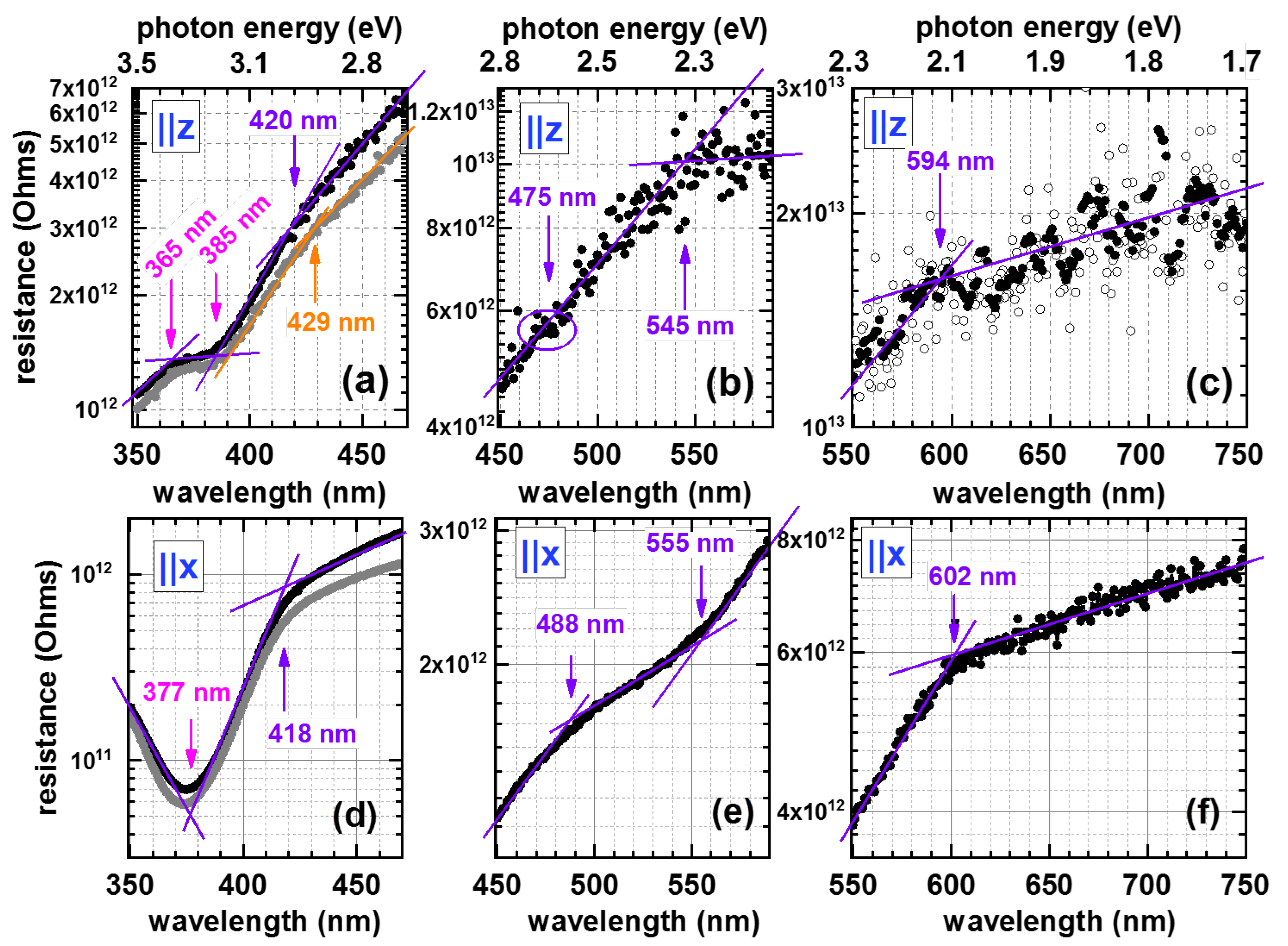
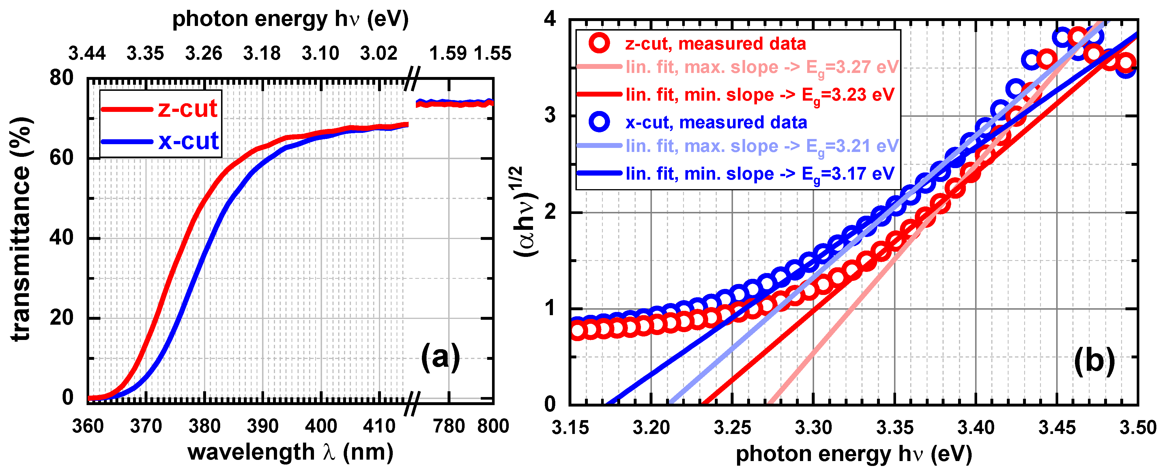
3.1. Wavelength Dependence of the Resistance between 350 and 750 nm

In order to get an overview of the energetic distribution of possible in-gap states as well as of the onset of bandgap absorption, we recorded the resistance as a function of wavelength, or, equivalently, of the excitation photon energy, along the polar axis (z-cut, depicted in Figure 2a–c) and, equally, perpendicular to the polar axis (x-cut, shown in Figure 2d–f), in order to check for anisotropic photoresponse. In principle, the technique of photoconductance (PC) spectrosocopy is able to reveal spectral features that are hidden to the (less sensitive) optical absorption spectroscopy. The technique is especially relevant for wide-gap materials being problematic for purely electrical gap-state spectroscopy methods. Indeed the PC spectra taken here unveil several peculiarities for the two perpendicularly cut SBN61 crystals as discussed below.
First, apart from an overall continuous decrease in the resistance (increase in the photoconductance) with increasing photon energy, there exist three points at distinct wavelengths in the sub-bandgap range at which either the slope changes or a small plateau appears. They clearly hint towards deep trap states and are marked with arrows in the semilog plot of Figure 2b,c,e,f: around 600 nm, between 550 and 560 nm, and around 480 nm, respectively. The features are also visible in the linear plots (Figure S4) and occur in both cuts. This is not surprising. Even though deep trap levels have been discussed mainly in conjunction with doping ions as their root, they may also originate from intrinsic point defects or, as is common to a number of complex oxides, from imperfections of the oxygen stoichiometry.
Second, in accordance with earlier works on mostly doped SBN, we find clear evidence for the existence of shallow trap states having a decisive impact on the photoconductance around 30–40 nm below the bandgap (Figure 2a,d): the resistance decreases quite sharply already around 420 nm, whereas the bandgap is at 389 nm (x-cut) or 381 nm (z-cut), as derived independently by transmittance spectra in conjunction with applying the Tauc method, see Figure 3.
Third, the points of slope change at 393 nm (z-cut) and at 398 nm (x-cut), which are only visible in the linear plots (Figure S4a,d) are related to the fundamental bandgap. As seen from the Tauc evaluation (see again Figure 3) and also shown in the literature [36], the bandgap is an indirect one. The features obtained from the resistance spectra suggest lower bandgaps than extracted from the transmittance spectra, but they agree in that the bandgap appears to be larger for the z-cut. With respect to this detail, results found in the literature are not completely comparable, since typically a bandgap anisotropy concerning different excitation-light polarizations sent to one crystal cut was observed there [10,13,37,38]. Nevertheless, all these former results show that the larger optical bandgap is obtained when the optical axis of the crystal is perpendicular to the electric-field vector of the incident light, which is observed here as well. That slightly different bandgaps are extracted from optical-excitation experiments is not surprising for anisotropic crystals in general, due to the strong interrelation between direction-dependent crystal symmetry, corresponding chemical bonds, resulting charge density distributions, and finally transition dipole moments. Going back to the features of the resistance-vs.-wavelength plots, one may speculate that a larger (possibly direct) bandgap is the origin of the last point of slope change on low-wavelength/high-energy side of the spectrum. However, the very long relaxation times after super-bandgap excitation may distort the spectrum in this range, which makes the interpretation questionable.
The energetic positions of all the features discussed above are listed in Table 2. While the slight variations of these positions depending on the type of the plot (linear vs. semilogarithmic) lie well within the spectral width of the illumination (∼10 nm), the several features appear clearly for both cuts. In the subbandgap range, they are systematically shifted to higher photon energies for the z-cut. Since the same tendency is found in the transmittance spectra, this fact again reflects the intrinsic anisotropic optical response. As mentioned above the even more anisotropic super-bandgap characteristics has to be interpreted with caution because of the very slow relaxation. In turn, this is the starting point for a more detailed analysis of full photoconductance transients at selected wavelengths, both below and above the bandgaps, as discussed next.

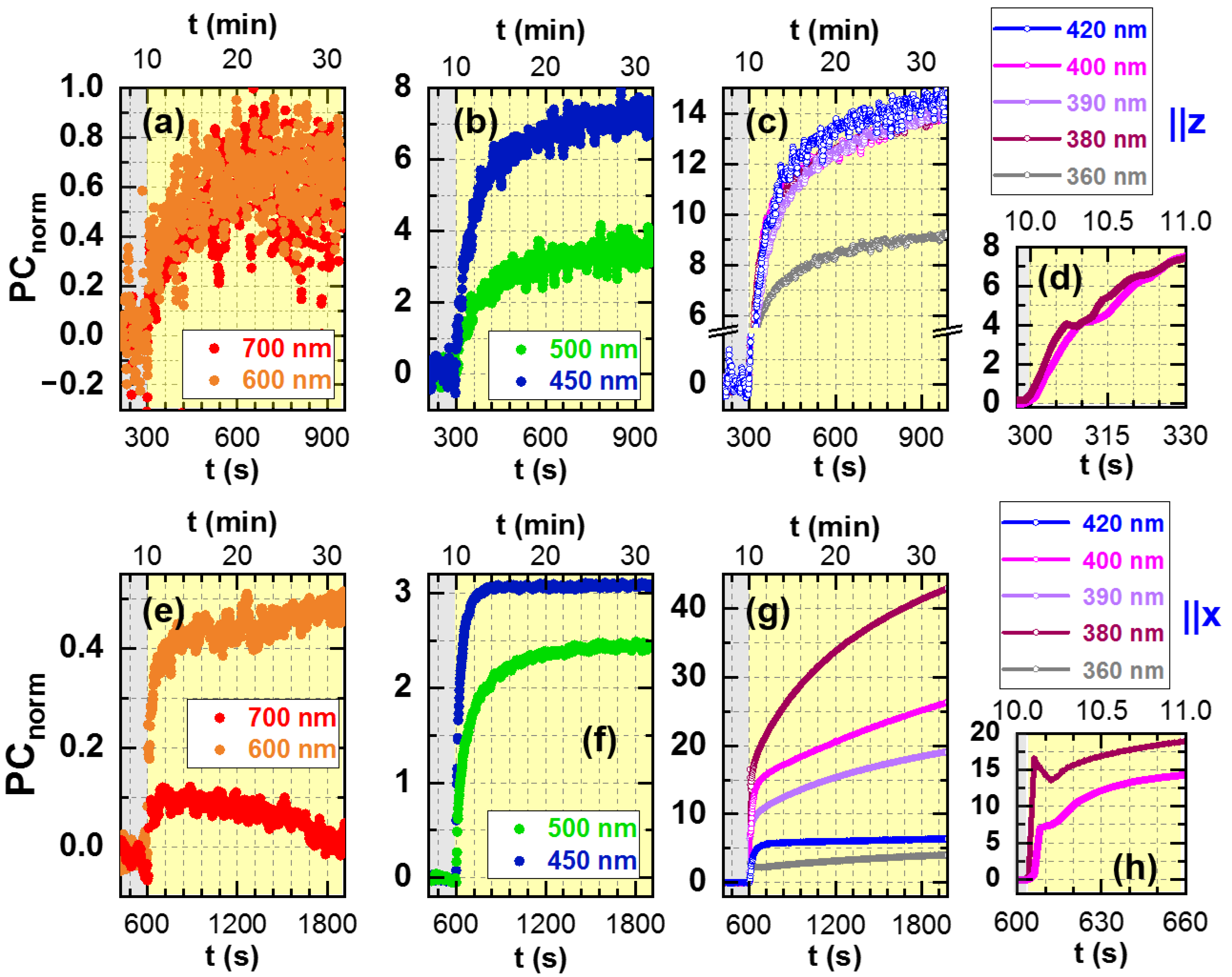
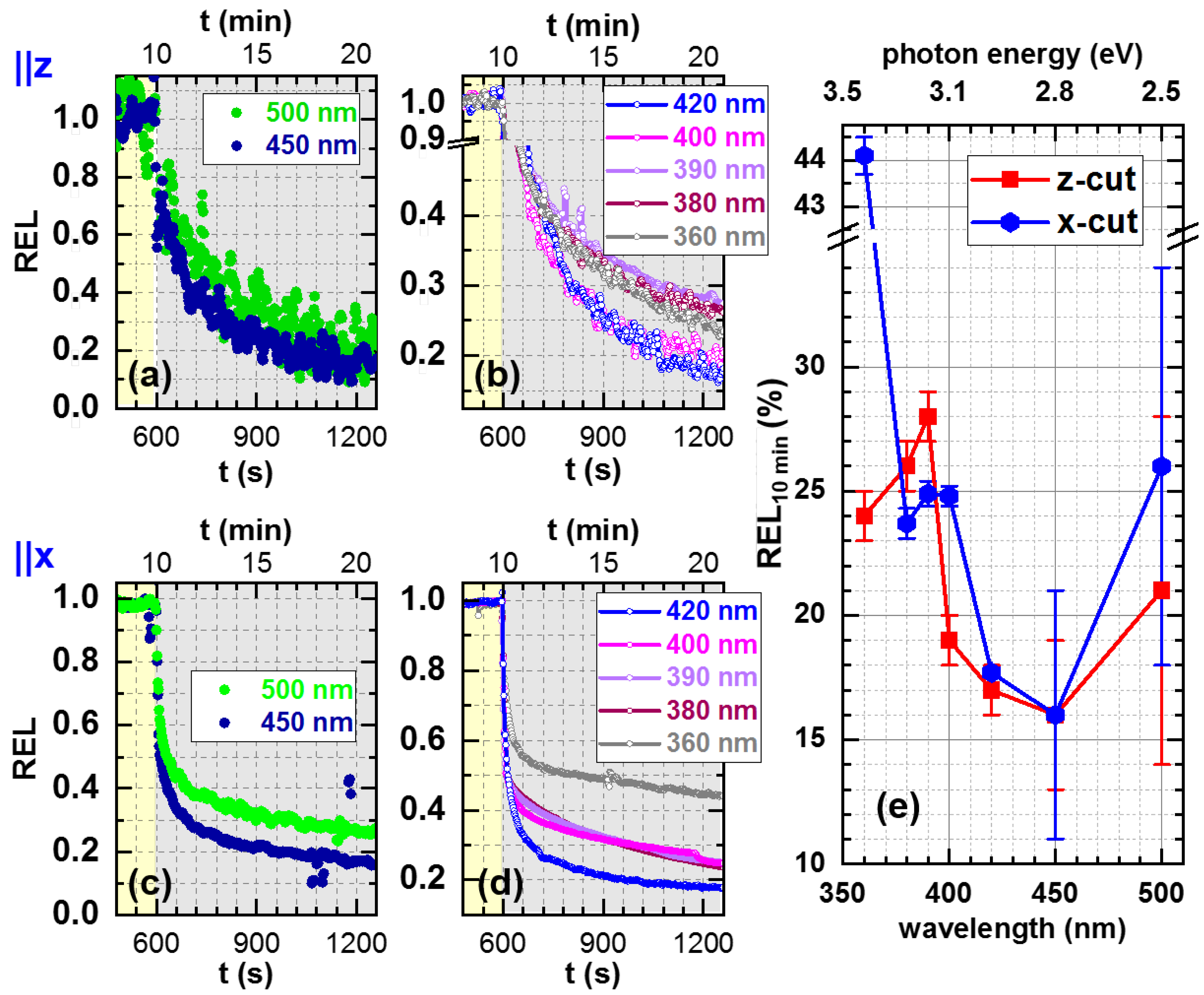
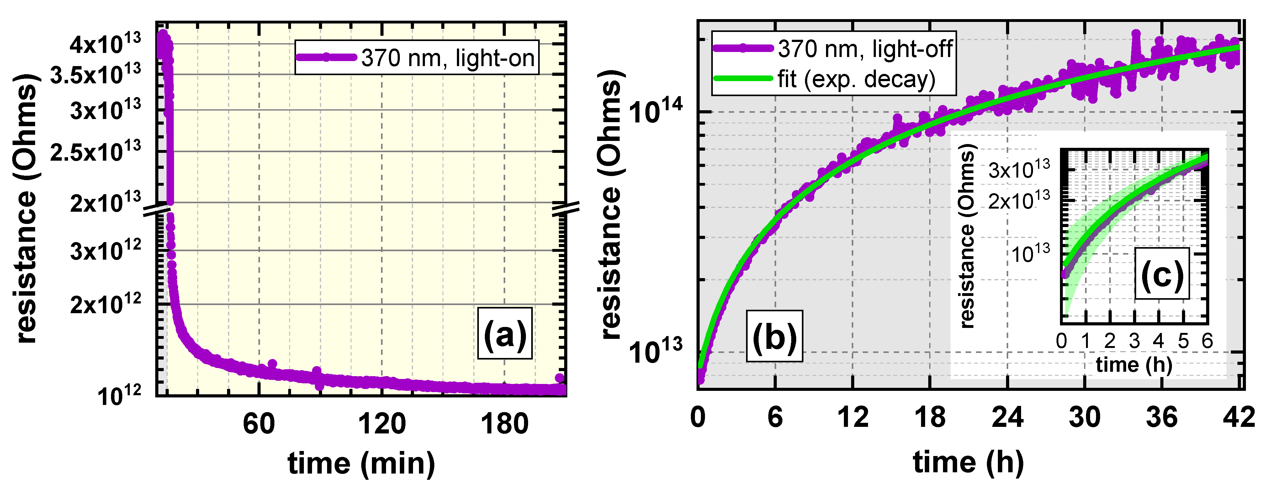
3.2. Resistance Relaxation Behavior upon Switching the Photoexcitation on and off

Since both the “teaser” experiment testing SBN’s resistance response to daylight (Figure S1) as well as the recordings of its photocondcutance spectra (Figure 2 and Figure S4) implied a rather slow reaction to illumination in the range of minutes at least, it appeared indispensable to explore this temporal behavior in more detail. Thus, full photoconductance transients at selected wavelengths were acquired following the protocol described in Section 2.
Figure 4 depicts the first 10 min of the light-on transients measured along (z-cut) and perpendicular to the polar axis (x-cut), respectively, with the measured resistance values being normalized according to Equation (1). At an 800 nm illumination, no significant photoresponse above noise level could be detected (not shown). For lower wavelengths, three “regimes” could be identified which were arranged in the subfigures (a)/(e), (b)/(f), (c)/(g), accordingly, and that exhibit the following characteristics:
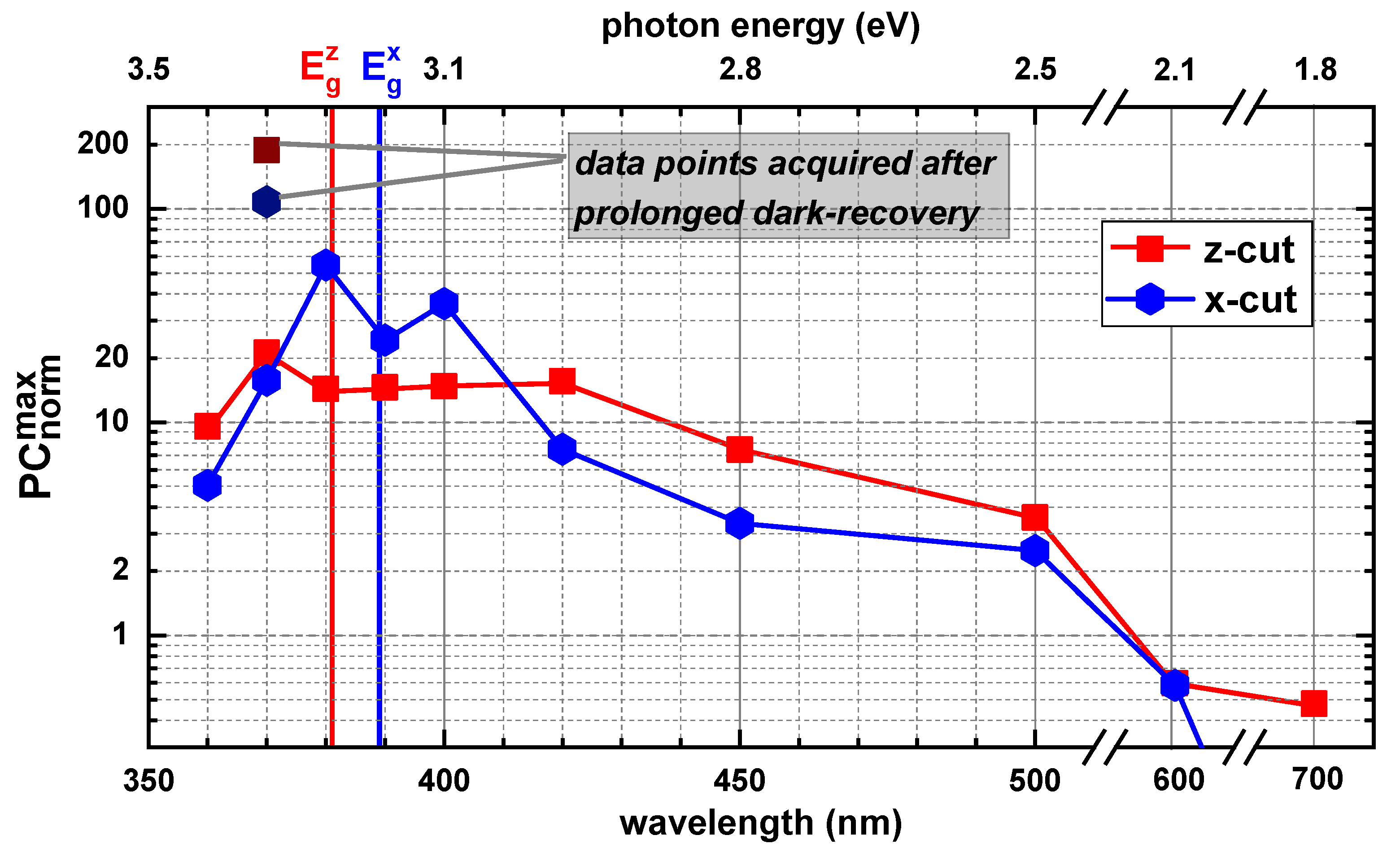
  • For 700 nm and 600 nm illumination (Figure 4a,e) a small but clear photoconductance not exceeding normalized values of 1 (z-cut) or 0.5 (x-cut) is observed.
  • With wavelengths of 500 nm or 450 nm (Figure 4b,f), a pronounced PC is achieved, corresponding to almost one order of magnitude of resistance decrease at 450 nm for the z-cut sample.
  • For excitation wavelengths of 420 nm and below (Figure 4c,g), PC values larger than 9 are measured, which is equivalent to a resistance drop of more than one order of magnitude. After a maximum around the bandgap, the effect again appears to weaken, the smaller the exciting wavelength gets (especially at 360 nm), probably due to the decreasing penetration depth of the photons and thus the lower probed volume.
When we qualitatively compare the behavior of the z-cut and the x-cut case from a more general point of view, a clear anisotropy is visible not only in the total strength of the photoresponse but also in its dynamics. For all wavelengths, the x-cut exhibits a faster initial rise of the PC, as compared to the z-cut SBN61, while in the region around the bandgap (389 nm and below) the light-on transients show a complex shape (exemplified in Figure 4h for 400 nm and 380 nm) indicating multiple charge transfer processes as observed in other complex oxides as well [39]. Neither the light-on nor the light-off transients could be fitted in a satisfactory manner assuming popular functions such as single, double, triple, or even stretched exponential models. This points to an entanglement of the underlying charge transfer processes, which might be modelled numerically only.
While Figure 4 shows the evolution of the PC within 10 min of illumination, Figure 5 plots the PC values reached after 60 min of illumination, when saturation is more complete (though–especially for wavelengths around the bandgaps–not fully completed), and gives us another comparative view on the two cuts, including further peculiarities concerning the anisotropy of SBN61’s photoresponse. The PC values measured for the x-cut sample show a much steeper increase when the wavelength approaches the bandgap, while the z-cut response is stronger in the sub-bandgap range but then hardly increases further close to the bandgap. The role of shallow states (starting around 420 nm excitation) appears to be much more prominent in the latter case. In summary, one can state that the qualitative evaluation of the photoconductance transients shows both the strong direction-dependent optical response as well as an anisotropic electronic transport behavior. The latter has also been reported and discussed, for example, in conjunction with the thermoelectric properties along different crystal cuts in a number of works in the past, see, e.g., [40,41].
Besides the information extracted from the data sets behind Figure 4, there are, in addition, two special single data points included in Figure 5, labelled as “data points acquired after a prolonged darkness period”. They indicate a much higher normalized photoconductance corresponding to a resistance difference between darkness and illumination of up to two orders of magnitude, and were achieved in a different measurement scenario. While the data points of Figure 4 were typically acquired with a recovery time in the dark of around 20 h between two measurement sessions, the recovery times for these two single data points were much longer, i.e., in the range of one week, corresponding to a more complete relaxation to the “true” dark resistance.
In all cases shown in Figure 4, we continued to record the resistance after having turned off the illumination. The resulting “light-off” transients obtained with the normalization of Equation (1), which reveal the relaxation behavior of the photoexcited carriers, are depicted for the first ten minutes in Figure S5, while Figure 6 shows the recovery behavior according to Equation (2). The majority of the transients in Figure S5 show a clear trend: a fast initial decay followed by a slow relaxation component, with none of the transients reaching zero PC, i.e., the initial dark resistance, within the time span considered here. An alternative insight can be obtained from the residual excess levels of Figure 6a–d and their summary in panel (e), where the R E L value after 10 min in the dark is plotted against the wavelength. The cases of 600 and 700 nm have been omitted because of large statistical errors. Typically, the excess conductance still lies in a range between 16 and 28% of the maximum excess conductance with the smallest value applying to 450 nm excitation. The anisotropic behavior can be seen from this plot particularly as a strong peculiarity for the x-cut sample after illumination at 360 nm. In this case, the R E L value after 10 min is 44% and is thus much higher than in all other cases, which may indeed indicate that a direct bandgap has been reached here—a speculation that was discussed already above in conjunction with the photoconductance spectrum of the x-cut sample.
To emphasize the obviously very slow photorelaxation, we acquired longer transients for the exemplarily chosen superbandgap wavelength of 370 nm in the z-cut sample, as illustrated for the light-on (observation period around 3 h) and the light-off case (observation period around 2 days) in Figure 7a,b, respectively. Despite the significantly enlarged monitoring periods, neither a saturation behavior of the resistance in the light-on transient can be seen, nor a full recovery of the dark resistance in the light-off transients. In spite of the difficulties with curve fitting, as described above, a simple single-exponential decay model in the form R = R 1 exp ( t / τ ) + R 0 f i n a l , with τ being the decay time constant and R 0 f i n a l the (final) asymptotically reached dark resistance, was employed to obtain at least a rough quantitative idea of a possible relaxation time constant for the light-off transient’s tail. The model fits the tail well (Figure 7b), but the initial decay less perfectly (inset, i.e., Figure 7c). A large half-life time constant in the range of (6 ± 3) days was extracted, as well as a dark resistance of R 0 f i n a l = (10 ± 5) × 1014 Ω .

3.3. Sublinear Intensity-Dependence

For doped SBN61, the sublinear intensity dependence of the photoconductivity in the form of Equation (3), has been discussed in conjunction with the underlying—especially deep- and shallow-trap-related—transport mechanism in the past, see, e.g., ref. [11] and refs. therein, in order to clarify in detail photorefractive processes aiming at writing of holographic gratings.
In the present study, which focuses on undoped SBN (that also exhibits signatures of both shallow and deep levels with a possible inter-trap charge transfer, as discussed in Section 3.1), this relation was recorded exemplarily for the z-cut sample at 500 nm and 380 nm wavelengths. The data shown in Figure 8 reveals the exponent x in Equation (3) to be 0.47 for the 500 nm (sub-bandgap) case and 0.80 for the 380 nm (super-bandgap) case. While the first value is indeed very similar to the findings in ref. [11] for a very slightly Ce-doped SBN61 crystal and strongly backs the hypothesis of a charge-exchange interplay between deep and shallow levels, as originally stated earlier in conjunction with photorefractive BaTiO3 [42,43], there seems to be no comparable data in the literature for super-bandgap excitation so far that could serve as a good reference.

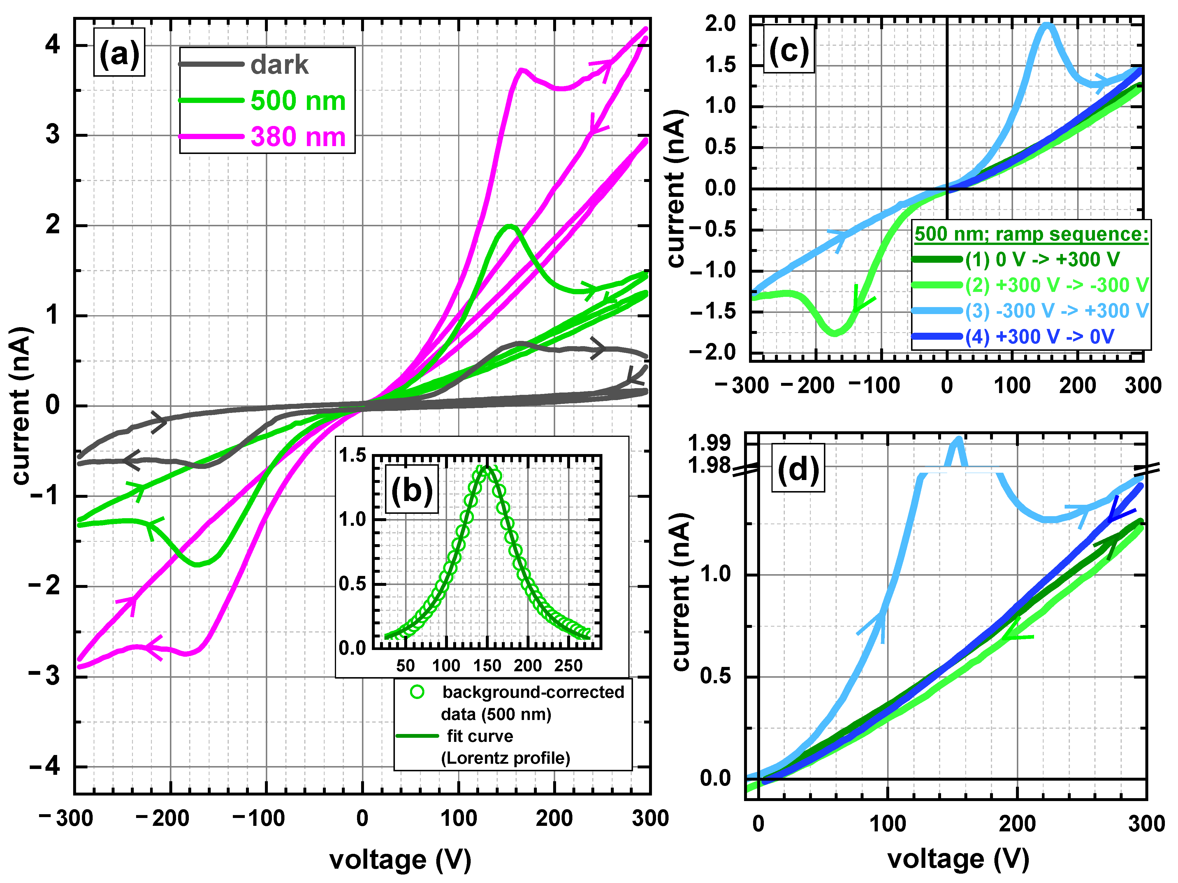
3.4. Current–Voltage Characteristics in the Dark and under Sub- and Super-Bandgap Light

As factors such as contact materials and resulting contact resistances have been discussed to influence the results of transport measurements in the past, we double-checked for this effect by analyzing the current–voltage characteristics in the dark over the range between ±100 V, i.e., not reaching the coercive field (literature values scatter between 2 and 3 kV/cm), and could verify an ohmic behavior, at least around the measuring voltage of 10 V used for all previously described investigations. Moreover, we found a hysteresis, as expected for a relaxor ferroelectric (cf. Figure S6).
In further experiments, the voltage range was enlarged to determine a possible influence of the illumination conditions on the coercive voltage (an effect that has been shown in a different context before [44]), i.e., the voltage at which ferroelectric switching takes place. Figure 9a gives a comparative view on the I-V characteristics in the dark and under sub- and super-bandgap illumination, in which switching events manifest themselves as current peaks. Qualitatively, the results are as expected: the general current level significantly rises with decreasing excitation wavelength. The coercive fields were extracted by peak fitting after background correction, exemplarily shown for the 500 nm case in Figure 9b. These were found to be 3 kV/cm for 500 nm illumination and 3.3 kV/cm for the two other cases, i.e., in the dark and under 380 nm illumination. The question, whether there is a real trend towards lower coercive fields upon sub-bandgap illumination, cannot be easily answered from these exemplary measurements and would need a much broader study. In all cases, the height of the switching peak is asymmetric with regard to the voltage ramp direction, as seen from Figure 9a and also from the close-up view of the 500 nm case, which illustrates the ramp directions, in Figure 9c. As accompanying measurements show, a number of additional parameters, such as ramping speed and direction, number of cycles (already described earlier in the literature [45]), or pre-illumination history also heavily influence the exact parameters (position, FWHM, height) of the current switching peaks as well. Thus, we are faced with a rather wide parameter space with the illumination parameters not necessarily being the most effective tuning parameters for that. However, this is a follow-up story not treated here.
Finally, note that the in-depth I-V measurements were carried out exclusively with the z-cut crystal. For the x-cut sample, only one measurement (dark, ±300 V) was realized, where, as expected a hysteresis, but no ferroelectric switching currents, i.e., displacement currents, were visible.

4. Summary and Outlook

In summary, the photoresponse of undoped z-cut and x-cut Sr0.61Ba0.39Nb2O6 single crystals, which turned out to be measurably photosensitive already under daylight, was investigated systematically. To date, most of the scientific activity into photoconductance (PC) measurements was dedicated to exploring and understanding the impact of doping ions on the electronic structure. In those studies, doping ions such as cerium or chromium, which are able to alter and improve certain non-linear optical properties such as the photorefractive response, were shown to have an effective influence on the photoconductivity. In contrast, the present work demonstrates that the undoped material is also photoconductive, not only under controlled illumination conditions but already under random daylight.
Four different measurement scenarios were employed to comprehensively characterize the photoconductance:
  • First, the wavelength dependence was recorded (“photoconductance spectroscopy”), which showed robust signatures of three different deep levels and a clear band of shallow states. At the current state of knowledge, one may speculate on the origin of these defect states: intrinsic point defects, oxygen vacancies, low-concentration impurity ions, and polaronic contributions are conceivable. For a further clarification, more comparative and comprehensive spectroscopic efforts are needed.
  • Second, the time evolution of the photoconductance upon switching the illumination on and off was monitored, i.e., “light-on” and “light-off” photoconductance transients at selected wavelengths were recorded in order to obtain insights to the relevant relaxation times. Though the failure of a number of analytical fit models—a phenomenon that was reported in the past for SBN in a slightly different context [37]—points towards complex and entangled multilevel charge transfer processes (which are not unusual for complex oxides in general) the tail of the long-term relaxation transient in the dark after super-bandgap illumination could be well described by a single time constant in the range of several days. The slow relaxation means that crystals which have not been stored in total darkness for a considerable time span are in a photoexcited state and do not show their true dark resistance.
  • Third, the intensity dependence appeared to be sublinear in accordance with earlier results on very weakly Ce-doped SBN.
  • Fourth, the wavelength was tested as a parameter being potentially able to tune the current–voltage characteristics including the coercive voltage in the z-cut crystal. Though the illumination wavelength—but also the pre-illumination history—has a clear influence on the current level and the coercive voltage, there are a number of other parameters, namely the direction and speed of the voltage ramp as well as the number of voltage cycles, which influence the exact shape of the current–voltage characteristics.
In conclusion, the latter result together with the ultralong photorelaxation time constants make undoped SBN61 challenging as an optoelectronic material in the sense of a material whose local or non-local electrical or coupled electrical–ferroelectric (f.i. ferroelectric-domain-related) properties are exactly and reproducibly tunable by light. Thus, at the current stage of knowledge, it seems that exploiting (doped) SBN’s non-linear optical properties stays the primary field of technological interest into this material. The present investigation closes a gap of fundamental knowledge on this complex-oxide compound. Furthermore, the present observations show that, in general, as for a number of other complex oxides, any optical analysis of SBN has to be interpreted with special care due to the somewhat “floating” conductance status resulting from previous illumination periods.

Supplementary Materials

The following are available online at https://www.mdpi.com/article/10.3390/cryst11070780/s1, Figure S1: Resistance decrease under daylight, Figure S2: PFM images of the SBN61 z-cut showing ferroelectric nanodomains, Figure S3: Temperature series of CSHG images of lithographically written domains in z-cut SBN61, Figure S4: Linear resistance-vs.-wavelength plots, Figure S5: Light-off transients of the normalized photoconductance, Figure S6: Current–voltage characteristics of z-cut SBN61 in the dark in the ±100 V range.

Author Contributions

Conceptualization, E.B.; methodology, E.B.; software, E.B., J.R. and M.R. (Matthias Roeper); validation, J.R., E.B., M.R. (Michael Rüsing) and L.M.E.; formal analysis, J.R. and E.B.; investigation, J.R., E.B., B.K., M.R. (Matthias Roeper) and L.I.I.; resources, L.I.I. and L.M.E.; data curation, E.B.; writing—original draft preparation, E.B., J.R. and L.I.I.; writing—review and editing, E.B., M.R. (Michael Rüsing) and L.M.E.; visualization, J.R. and E.B.; supervision, E.B. and L.M.E.; project administration, E.B. and L.M.E.; funding acquisition, L.I.I. and L.M.E. All authors have read and agreed to the published version of the manuscript.

Funding

This research was funded by VolkswagenStiftung (grant no. 90 261), Deutsche Forschungsgemeinschaft (DFG) via CRC 1415 (project no. 417590517) and FOR 5044 (project no. 426703838).

Institutional Review Board Statement

Not applicable.

Informed Consent Statement

Not applicable.

Data Availability Statement

The data presented in this study are available on request from the corresponding author.

Acknowledgments

E.B. thanks S. Grafström for many valuable discussions on the manuscript as well as T. Paulat and H. Beccard for support in the laboratory concerning PFM and CSHG measurements.

Conflicts of Interest

The authors declare no conflict of interest.

References

  1. Ivleva, L.I.; Kozlova, N.S.; Zabelina, E.V. Study of the temperature dependence of the electrical conductivity in strontium-barium niobate crystals with different dopants. Crystallogr. Rep. 2007, 52, 328–331. [Google Scholar] [CrossRef]
  2. Bhatt, R.; Soharab, M.; Bhaumik, I.; Verma, P.; Sajith, B.; Saxena, A.; Karnal, A. Effect of reduction on the optical properties of Sr0.61Ba0.39Nb2O6 single crystals grown by optical floating zone technique. J. Alloys Compd. 2019, 810, 151818. [Google Scholar] [CrossRef]
  3. Podlozhenov, S.; Graetsch, H.A.; Ulex, M.; Schneider, J.; Wöhlecke, M.; Betzler, K. Structure of strontium barium niobate SrxBa1−xNb2O6 (SBN) in the composition range 0.32≤x≤0.82. Acta Cryst. 2006, B62, 960–965. [Google Scholar] [CrossRef] [PubMed] [Green Version]
  4. Kleemann, W. The relaxor enigma—Charge disorder and random fields in ferroelectrics. J. Mater. Sci. 2006, 41, 129–136. [Google Scholar] [CrossRef]
  5. Shvartsman, V.V.; Kleemann, W.; Łukasiewicz, T.; Dec, J. Nanopolar structure in SrxBa1−xNb2O6 single crystals tuned by Sr/Ba ratio and investigated by piezoelectric force microscopy. Phys. Rev. B 2008, 77, 054105. [Google Scholar] [CrossRef]
  6. Shur, V.Y.; Shikhova, V.A.; Ievlev, A.V.; Zelenovskiy, P.S.; Neradovskiy, M.M.; Pelegov, D.V.; Ivleva, L.I. Nanodomain structures formation during polarization reversal in uniform electric field in strontium barium niobate single crystals. J. Appl. Phys. 2012, 112, 064117. [Google Scholar] [CrossRef] [Green Version]
  7. Shur, V.; Shikhova, V.; Alikin, D.; Lebedev, V.; Ivleva, L.; Dec, J.; Lupascu, D.; Shvartsman, V. Temperature Effect on the Stability of the Polarized State Created by Local Electric Fields in Strontium Barium Niobate Single Crystals. Sci. Rep. 2017, 7, 125. [Google Scholar] [CrossRef] [Green Version]
  8. Shikhova, V.A.; Fedorovyh, V.V.; Turygin, A.P.; Gimadeeva, L.V.; Chezganov, D.S.; Vlasov, E.O.; Alikin, D.O.; Ivleva, L.I.; Kholkin, A.L.; Shur, V.Y. Local switching in SBN:Ni single crystals with various initial domain states. Ferroelectrics 2018, 525, 100–107. [Google Scholar] [CrossRef]
  9. Chezganov, D.S.; Shikhova, V.A.; Fedorovyh, V.V.; Vlasov, E.O.; Chuvakova, M.A.; Nebogatikov, M.S.; Zelenovskiy, P.S.; Kholkin, A.L.; Ivleva, L.I.; Shur, V.Y. Domain Switching by Electron Beam Irradiation in SBN61:Ce Single Crystals Covered by Dielectric Layer. IEEE Trans. Ultrason. Ferroelectr. Freq. Control 2020, 67, 191–196. [Google Scholar] [CrossRef] [PubMed]
  10. Buse, K.; van Stevendaal, U.; Pankrath, R.; Kratzig, E. Light-induced charge transport properties of Sr0.61Ba0.39Nb2O6:Ce crystals. J. Opt. Soc. Am. B 1996, 13, 1461–1467. [Google Scholar] [CrossRef]
  11. Buse, K.; Gerwens, A.; Wevering, S.; Kratzig, E. Charge-transport parameters of photorefractive strontium-barium niobate crystals doped with cerium. J. Opt. Soc. Am. B 1998, 15, 1674–1677. [Google Scholar] [CrossRef]
  12. Wevering, S.; Buse, K.; Simon, R.; Pankrath, R.; Kratzig, E. Time-resolved measurements of photoconductivity in cerium-doped photorefractive strontium-barium niobate using nanosecond light pulses. Opt. Commun. 1998, 148, 85–89. [Google Scholar] [CrossRef]
  13. Dörfler, U.; Granzow, A.; Woike, T.; Wöhlecke, M.; Imlau, M.; Pankrath, R. Intensity and wavelength dependence of the photoconductivity in Cr-doped Sr0.61Ba0.39Nb2O6. Eur. Phys. J. B 2004, 38, 19–24. [Google Scholar] [CrossRef]
  14. Demirbilek, R.; Kılıç, M. The parameters that play role in numerical parameter variation in two-center holographic recording in photorefractive lithium niobate (LiNbO3) and strontium barium niobate (SrxBa1−xNb2O6). Phys. Status Solidi A 2013, 210, 1641–1646. [Google Scholar] [CrossRef]
  15. Gladkiĭ, V.V.; Kirikov, V.A.; Volk, T.R.; Ivanova, E.S.; Ivleva, L.I. Polarization kinetics of a photosensitive relaxor ferroelectric. Phys. Solid State 2005, 47, 298–304. [Google Scholar] [CrossRef]
  16. Gladkiĭ, V.V.; Kirikov, V.A.; Ivanova, E.S.; Volk, T.R. On the permittivity of barium strontium niobate, a photosensitive relaxor ferroelectric. Phys. Solid State 2006, 48, 1929–1932. [Google Scholar] [CrossRef]
  17. Gladkiĭ, V.V.; Kirikov, V.A.; Ivanova, E.S.; Volk, T.R. Reversible permittivity of a photosensitive relaxor ferroelectric. Phy. Solid State 2006, 48, 2146–2149. [Google Scholar] [CrossRef]
  18. Gladkiĭ, V.V.; Kirikov, V.A.; Ivanova, E.S.; Volk, T.R. Quasi-static loops of the dielectric hysteresis for a photosensitive relaxor ferroelectric crystal in the temperature range of the diffuse phase transition. Phys. Solid State 2007, 49, 930–935. [Google Scholar] [CrossRef]
  19. Gladkiĭ, V.V.; Ivanova, E.S.; Volk, T.R. Depolarization in a photosensitive relaxor ferroelectric. Phys. Solid State 2007, 49, 2148–2153. [Google Scholar] [CrossRef]
  20. Fan, D.; Zhu, J.; Wang, X.; Wang, S.; Liu, Y.; Chen, R.; Feng, Z.; Fan, F.; Li, C. Dual Extraction of Photogenerated Electrons and Holes from a Ferroelectric Sr0.5Ba0.5Nb2O6 Semiconductor. ACS Appl. Mater. Interfaces 2016, 8, 13857–13864. [Google Scholar] [CrossRef]
  21. Fan, D.; Chong, R.; Fan, F.; Wang, X.; Li, C.; Feng, Z. A tetragonal tungsten bronze-type photocatalyst: Ferro-paraelectric phase transition and photocatalysis. Chin. J. Catal. 2016, 37, 1257–1262. [Google Scholar] [CrossRef]
  22. Barnes, E.; Alberts, E.M.; Mimun, L.C.; Brame, J.A.; Warner, C.M.; Harmon, A.R.; Poda, A.R. Photoinduced Metallic Particle Growth on Single-Crystal Relaxor Ferroelectric Strontium Barium Niobate. J. Phys. Chem. C 2018, 122, 5590–5598. [Google Scholar] [CrossRef]
  23. Ivleva, L.; Kuz’minov, Y.; Osiko, V.; Polozkov, N. The growth of multicomponent oxide single crystals by Stepanov’s technique. J. Cryst. Growth 1987, 82, 168–176. [Google Scholar] [CrossRef]
  24. Ivleva, L.; Bogodaev, N.; Polozkov, N.; Osiko, V. Growth of SBN single crystals by Stepanov technique for photorefractive applications. Opt. Mater. 1995, 4, 168–173. [Google Scholar] [CrossRef]
  25. Ivleva, L.I. Physicochemical and Technological Peculiarities of Multicomponent Oxide Crystal Growth from Melt by Modified Stepanov Technique. Bull. Russ. Acad. Sci. Phys. 2009, 73, 1338–1340. [Google Scholar] [CrossRef]
  26. Kuz’micheva, G.M.; Ivleva, L.I.; Kaurova, I.A.; Rybakov, V.B. Structural peculiarities and point defects of undoped and Cr- and Ni-doped SrxBa1−xNb2O6 crystals. Acta Mater. 2014, 70, 208–217. [Google Scholar] [CrossRef]
  27. Kaurova, I.A.; Kuz’micheva, G.M.; Ivleva, L.I.; Chernyshev, V.V.; Rybakov, V.B.; Domoroshchina, E.N. X-ray powder diffraction methods for the determination of composition and structural parameters of Cr- and Ni-doped Sr0.61Ba0.39Nb2O6 crystals. J. Alloys Compd. 2015, 638, 159–165. [Google Scholar] [CrossRef]
  28. Kuz’micheva, G.M.; Ivleva, L.I.; Kaurova, I.A.; Rybakov, V.B.; Cousson, A. Structure and real composition of undoped and Cr- and Ni-doped Sr0.61Ba0.39Nb2O6 single crystals. Struct. Chem. 2016, 27, 1623–1634. [Google Scholar] [CrossRef]
  29. Shvartsman, V.V.; Gobeljic, D.; Dec, J.; Lupascu, D.C. A Piezoresponse Force Microscopy Study of CaxBa1−xNb2O6 Single Crystals. Materials 2017, 10, 1032. [Google Scholar] [CrossRef] [PubMed] [Green Version]
  30. Pavlenko, A.; Ivleva, L.; Stryukov, D.; Kovtun, A.; Anokhin, A.; Lykov, P. Synthesis, Structure, and Dielectric Characteristics of Sr0.61Ba0.39Nb2O6 Single Crystals and Thin Films. Phys. Solid State 2019, 61, 244–248. [Google Scholar] [CrossRef]
  31. Beyreuther, E.; Thiessen, A.; Becherer, J.; Grafström, S.; Dörr, K.; Eng, L. Probing electronic defect states in manganite/SrTiO3 heterostructures by surface photovoltage spectroscopy. Mater. Sci. Eng. B 2011, 176, 446–452. [Google Scholar] [CrossRef]
  32. Bhatt, V.; Kumar, M.; Kim, J.; Chung, H.J.; Yun, J.H. Persistent photoconductivity in Al-doped ZnO photoconductors under air, nitrogen and oxygen ambience: Role of oxygen vacancies induced DX centers. Ceram. Int. 2019, 45, 8561–8570. [Google Scholar] [CrossRef]
  33. Tauc, J.; Grigorovici, R.; Vancu, A. Optical Properties and Electronic Structure of Amorphous Germanium. Phys. Status Solidi B 1966, 15, 627–637. [Google Scholar] [CrossRef]
  34. Szczyrbowski, J.; Dietrich, A.; Hoffmann, H. Optical Properties of RF-Sputtered Indium Oxide Films. Phys. Status Solidi A 1982, 69, 217–226. [Google Scholar] [CrossRef]
  35. Viezbicke, B.D.; Patel, S.; Davis, B.E.; Birnie, D.P., III. Evaluation of the Tauc method for optical absorption edge determination: ZnO thin films as a model system. Phys. Status Solidi B 2015, 252, 1700–1710. [Google Scholar] [CrossRef]
  36. Andriyevsky, B.; Patryn, A.; Dorywalski, K.; Cobet, C.; Piasecki, M.; Kityk, I.; Esser, N.; Łukasiewicz, T.; Dec, J. Electronic and Optical Properties of Strontium Barium Niobate Single Crystals. Ferroelectrics 2012, 426, 194–205. [Google Scholar] [CrossRef]
  37. Gao, M.; Kapphan, S.; Porcher, S.; Pankrath, R. Experimental study of NIR absorption due to Nb4+ polarons in pure and Cr- or Ce-doped SBN crystals. J. Phys. Condens. Matter 1999, 11, 4913–4924. [Google Scholar] [CrossRef]
  38. Primrose, M.S.; Toulouse, J.; Bock, J.; Randall, C. Raman spectroscopy study of reduced strontium barium niobate (SBN61) and hints of supergrowth or intergrowth structures. J. Raman Spectrosc. 2018, 49, 1849–1859. [Google Scholar] [CrossRef]
  39. Beyreuther, E.; Becherer, J.; Thiessen, A.; Grafström, S.; Eng, L. Electronic surface properties of SrTiO3 derived from a surface photovoltage study. Surf. Sci. 2013, 612, 1–9. [Google Scholar] [CrossRef]
  40. Lee, S.; Wilke, R.H.T.; Trolier-McKinstry, S.; Zhang, S.; Randall, C.A. SrxBa1−xNb2O6-δ Ferroelectric-thermoelectrics: Crystal anisotropy, conduction mechanism, and power factor. Appl. Phys. Lett. 2010, 96, 031910. [Google Scholar] [CrossRef]
  41. Li, Y.; Liu, J.; Chen, Y.; Zhang, X.; Wang, X.; Wang, F.; Su, W.; Li, J.; Wang, C. Oxygen vacancy induced strong anisotropy of the thermoelectric properties of strontium barium niobate. Comput. Mater. Sci. 2018, 155, 393–399. [Google Scholar] [CrossRef]
  42. Holtmann, L.; Unland, M.; Krätzig, E.; Godefroy, G. Conductivity and Light-Induced Absorption in BaTiO3. Appl. Phys. A 1990, 51, 13–15. [Google Scholar] [CrossRef]
  43. Mahgerefteh, D.; Feinberg, J. Explanation of the Apparent Sublinear Photoconductivity of Photorefractive Barium Titanate. Phys. Rev. Lett. 1990, 64, 2195–2198. [Google Scholar] [CrossRef] [PubMed]
  44. Smith, P.G.R.; Eason, R.W. Influence of light on the coercive field of repoled strontium barium niobate: The role of secondary repoling. Appl. Phys. Lett. 1996, 69, 1509–1511. [Google Scholar] [CrossRef]
  45. Gladkiĭ, V.; Kirikov, V.; Nekhlyudov, S.; Volk, T.; Ivleva, L. Polarization and depolarization of relaxor ferroelectric strontium barium niobate. Phys. Solid State 2000, 42, 1334–1340. [Google Scholar] [CrossRef]
Figure 1. (a) Scheme of the electrical measurement configuration. For the realization of the optical beam path between white-light source and final focus on the sample see ref. [31]. Panels (b,c) illustrate the light incidence (wave vector k) towards the z- and x-cut SBN crystal, respectively, with blue arrows indicating the axis of (ferro-)electric polarization (vector P) in the sample, which is in this case equal to the optical axis. The blue coordinate systems refer to the crystal axes. Note that the electric-field vector E of the unpolarized light is perpendicular to the optical/polar axis z of the crystal in case (b)/z-cut and lies in the yz plane of the crystal in case (c)/x-cut.
Crystals 11 00780 g001
Figure 2. Comparative semilogarithmic resistance plots with spectral features: While subfigures (ac) show the wavelength dependence of the resistance measured along the polar axis (z-cut sample), the subfigures (df) depict the corresponding data recorded for the x-cut sample. The data was acquired within three overlapping partial spectra beginning at the high-wavelength end in all cases. Points of slope change or discontinuities in the from of small plateaus are indicated by arrows and are summarized in Table 2. For the subspectra (a,d) the two different curves (black vs. grey) demonstrate the degree of reproducibility; for case (c) a smoothed curve (filled circles) is shown alongside with the quite scattering original data (open circles). The extracted spectral features were compared with those extracted from the corresponding linear plots, which can be found in Figure S4.
Crystals 11 00780 g002
Figure 3. (a) Optical transmittance spectra of the x-cut and z-cut SBN61 crystals; (b) derivation of the respective bandgaps, which appeared to be indirect, by the Tauc method [33,34,35].
Crystals 11 00780 g003
Figure 4. Temporal behavior of the normalized PC–light-on transients of the (ad) z-cut and (eh) x-cut SBN61 samples for selected wavelengths: greyish background indicating darkness and yellowish background indicating illumination. Subfigures (d,h), which are close-up fews of the first 60 s upon illumination for the cases of 380 nm and 400 nm, illustrate that especially for the x-cut case obviously multiple charge carrier transitions add up to a complex transient behavior.
Crystals 11 00780 g004
Figure 5. Semi-logarithmic overview of the normalized PC achieved after a 60 min illumination period (averaged over the last 10 min of this 60 min illumination interval) for all selected wavelengths and for both crystal cuts. Note that the value at 700 nm for the x-cut was omitted, because it might not be reliable, since the maximum PC is not achieved after 60 min in that case, but earlier (cf. Figure 4e). The two darker colored data points (recorded at 370 nm) indicate much higher PC values and were acquired after a one-week- instead of a 20-h dark recovery.
Crystals 11 00780 g005
Figure 6. Light-off transients (calculated employing the normalization of Equation (2)) of the (a,b) z-cut and (c,d) the x-cut SBN61 sample for selected wavelengths, showing the development of the residual excess level of the conductance within the first 10 minutes after the end of a 60-min illumination interval (illustrated in the two previous Figure 4 and Figure 5). Greyish background indicates darkness and yellowish background indicates illumination. Subfigure (e) shows the residual excess level after 10 min in the dark, denoted as R E L 10 min , plotted against the wavelength and constitutes a kind of a counterpart to Figure 5.
Crystals 11 00780 g006
Figure 7. Long-term transients of the resistance as acquired exemplarily upon 370 nm super-bandgap illumination: (a) Light-on transient recorded for more than 3 h; (b) tail of the light-off transient recorded for 42 h with a single-exponential fit indicating a time constant in the range of 213 h or approximately 9 days (equivalent to a “half-life” time constant of 6 days) with inset (c) showing a close-up view of the fit and 95%-confidence bands for the time regime short after shadowing the sample.
Crystals 11 00780 g007
Figure 8. Double-logarithmic conductance-vs.-intensity plots of the z-cut SBN61 crystal at 500 nm and 380 nm excitation wavelengths with dots symbolizing the measured values, averaged as described in Section 2, and straight lines showing the corresponding sublinear fit curves.
Crystals 11 00780 g008
Figure 9. (a) Comparison of the current–voltage characteristics of the SBN61 crystal measured along the polar z-axis between ±300 V in the dark (grey) and at 500 nm (green) as well as 380 nm (magenta) illumination, the latter two with a photon flux of 6.8 × 10 15 s−1. (b) Extraction of the coercive voltage by background correction and peak fitting for the positive-branch switching peak with 500 nm illumination. (c) Zoomed view of the IV-characteristics under 500 nm illumination with the different colors symbolizing the order of the applied voltage ramps. (d) As the close-up view of the first quadrant of subfigure (c) shows, there is no ferroelectric switching upon the initial ramp (dark green), since the ramp direction is parallel to the initial polarization direction in this case.
Crystals 11 00780 g009
Table 1. Measurement details for the photoconductance spectra: start and end wavelengths (photon energies), cutoff wavelengths of the respective edge filters, and the blaze wavelengths of the monochromator gratings for the three overlapping partial spectra.
Wavelength RangeEnergy RangeFilter: λ cutoff Grating: λ blaze
(nm)(eV)(nm)(nm)
750–5501.55–2.25550750
600–4502.07–2.76395400
500–3502.48–3.54305400
Table 2. Summary of energetic positions (all numbers in nanometers) of spectral features as extracted from the resistance-vs.-wavelength plots of Figure 2 and Figure S4. Numbers in brackets refer to plateaus, all other numbers to points of slope change. Whenever two values are given, two different partial spectra were compared in order to asses the typical error range. For comparison, the bandgap values from the transmittance measurements were added as well (cf. Figure 3).
AssignmentZ-CutX-Cut
LinearLogarithmicLinearLogarithmic
direct(?) bandgap361365369
fundamental bandgap393385398(377)
bandgap from transmittance381 ± 3389 ± 3
shallow states(435)420/429424/422418
(“blue”) deep level(476)(475)482488
(“green”) deep level553545558555
(“red”) deep level599594601602
Publisher’s Note: MDPI stays neutral with regard to jurisdictional claims in published maps and institutional affiliations.

