Article

High-Quality All-Inorganic Perovskite CsPbBr3 Quantum Dots Emitter Prepared by a Simple Purified Method and Applications of Light-Emitting Diodes

1
Department of Electro-Optical Engineering, National Taipei University of Technology, Taipei 10608, Taiwan
2
Department of Electrical Engineering, China University of Science and Technology, Taipei 11581, Taiwan
3
Department of Electronic Engineering, Ming Chi University of Technology, New Taipei City 24301, Taiwan
*
Authors to whom correspondence should be addressed.
Energies 2019, 12(18), 3507; https://doi.org/10.3390/en12183507
Submission received: 7 August 2019 / Revised: 5 September 2019 / Accepted: 6 September 2019 / Published: 11 September 2019

Abstract

:
High-quality perovskite CsPbBr3 quantum dots (QDs-CsPbBr3) were prepared using the ultrasonic oscillation method, which is simple and provides variable yield according to requirements. The emission spectra over a large portion of the visible spectral region (450–650 nm) of QD-CsPbX3 (X = Cl, Br, and I) have tunable compositions that can be halide exchanged using the halide anion exchange technique and quantum size-effects. A strong peak with high intensity of (200) lattice plane of purified QDs-CsPbBr3 film is obtained, confirming the formation of an orthorhombic perovskite crystal structure of the Pnma space group. The photoluminescence of QDs-CsPbBr3 was characterized using a narrow line-width emission of 20 nm, with high quantum yields of up to 99.2%, and radioactive lifetime increasing to 26 ns. Finally, through the excellent advantages of QDs-CsPbBr3 mentioned above, purified perovskite QDs-CsPbBr3 as an active layer was utilized in perovskite quantum dot light-emitting diodes structure applications. As a result, the perovskite QDs-CsPbBr3 light-emitting diodes (LEDs) exhibits a turn-on voltage of 7 V and a maximum luminance of 5.1 cd/m2.

1. Introduction

All-inorganic cesium lead halide perovskite colloidal quantum dots (QDs-CsPbX3, X = Cl, Br, I) possess excellent optical properties such as broadband absorption, high photoluminescence quantum yield (PLQY) of 50–90%, narrow emission bandwidth of 12–42 nm (from blue to red), tunable emission wavelength of 400–700 nm, as well as a wide color gamut of about 110% national television system committee (NTSC) [1,2,3,4,5,6,7,8]. These properties make it one of the most promising luminescent materials, showing great application prospects in light-emitting diodes (LEDs) [9,10], photodetector [11,12], photovoltaics [13,14], lasers [15,16], and color converters [17,18]. At present, the inorganic perovskite QDs-CsPbX3 preparation methods mainly include a high temperature hot injection method and a room temperature precipitation synthesis method. High-yield, high-crystallinity QDs-CsPbX3 (X = Cl, Br, I) can be obtained using the high-temperature hot injection method, however, they also need to be synthesized in an inert atmosphere with temperatures of about 140–160 °C. The room temperature precipitation synthesis method can synthesize CsPbX3 (X = Cl, Br, I) at room temperature [19], it is difficult to control the growth process and further adjust the luminescence properties due to the excessively intense and rapid reaction.
Today metal organic halide CH3NH3PbX3 (X = C1, Br, I) perovskites are more commonly used in colloidal quantum dot (QD)-based light-emitting diode (QD-LED) devices [20,21,22,23,24,25] and other optoelectronic devices [26,27,28,29]. Tan et al. first reported in 2014 the application of trihalide organic–inorganic perovskite materials on LED devices, in which the external quantum efficiency (EQE) was 0.1% at 517 nm green wavelength [20]. Subsequently, interface engineering and perovskite nanostructuring optimization was used to improve PLQY of the organic–inorganic perovskite material, which benefits the EQE performance enhancement of LEDs, increasing to over 8.53% [22]. Compared with metal organic halide CH3NH3PbX3 (X = C1, Br, I) perovskites, there are few reports on the preparation of LED devices with all inorganic CsPbX3 (X = C1, Br, I) perovskite. Kovalenko et al. reported a simple colloidal synthesis method for QDs-CsPbX3 at high temperature in 2015, which exhibited a high PLQY of more than 90% [1]. The EQE of the first reported CsPbBr3-based perovskite quantum dot used in LED device from Zeng et al. is only 0.12% [30]. Afterward, Pan et al. developed the highly stable QDs-CsPbX3 films with a short ligand di-dodecyl dimethyl ammonium bromide (DDAB) containing a Br anion on the ligand exchange that promotes carrier transport in the QD films and enables fabrication of the CsPbBr3-based perovskite QD-LEDs, with an EQE of 3.0% [31]. Zeng et al. proposed using ligand density control to balance surface passivation and carrier injection, as well as recycling treatment on QDs with mixed solvent to achieve efficient solution-processed CsPbBr3 QD-LEDs, which have a 50-fold EQE improvement (up to 6.27%) [32]. Furthermore, it was confirmed that the ester solvent washing process after the ligand exchange can remove impurities such as excess ligand and reaction solvent [33]. Consequently, surface ligand engineering and the purification process are important for obtaining high quality perovskite QDs [34,35].
Herein, the purpose of this study is to use quantum dots (QDs) as the emission layer of the quantum dot LEDs. Firstly, the perovskite QDs-CsPbBr3 solution was synthesized, and can be successfully spin-coated on the ITO substrate using purification technology. The QD surface coating pattern is an important factor affecting QD-LED equality and confirming whether it emits light. Surface ligands have a dual effect on quantum dots. One is that a large amount of ligand is sufficient to provide surface purification, which eliminates surface defects, thereby increasing QD solution quantum yield and stability. The other is that the excess ligand will form insulation due to oleic acid poor conductivity. Excess oleic acid has a negative effect on charge injection inside the QD-LEDs. We investigate the material and optical properties of unpurified and purified QDs-CsPbBr3 via a purification procedure. Finally, by taking advantage of these outstanding optical properties, the QDs-CsPbBr3 was successfully applied in color purity perovskite QD-LEDs.

2. Materials and Methods

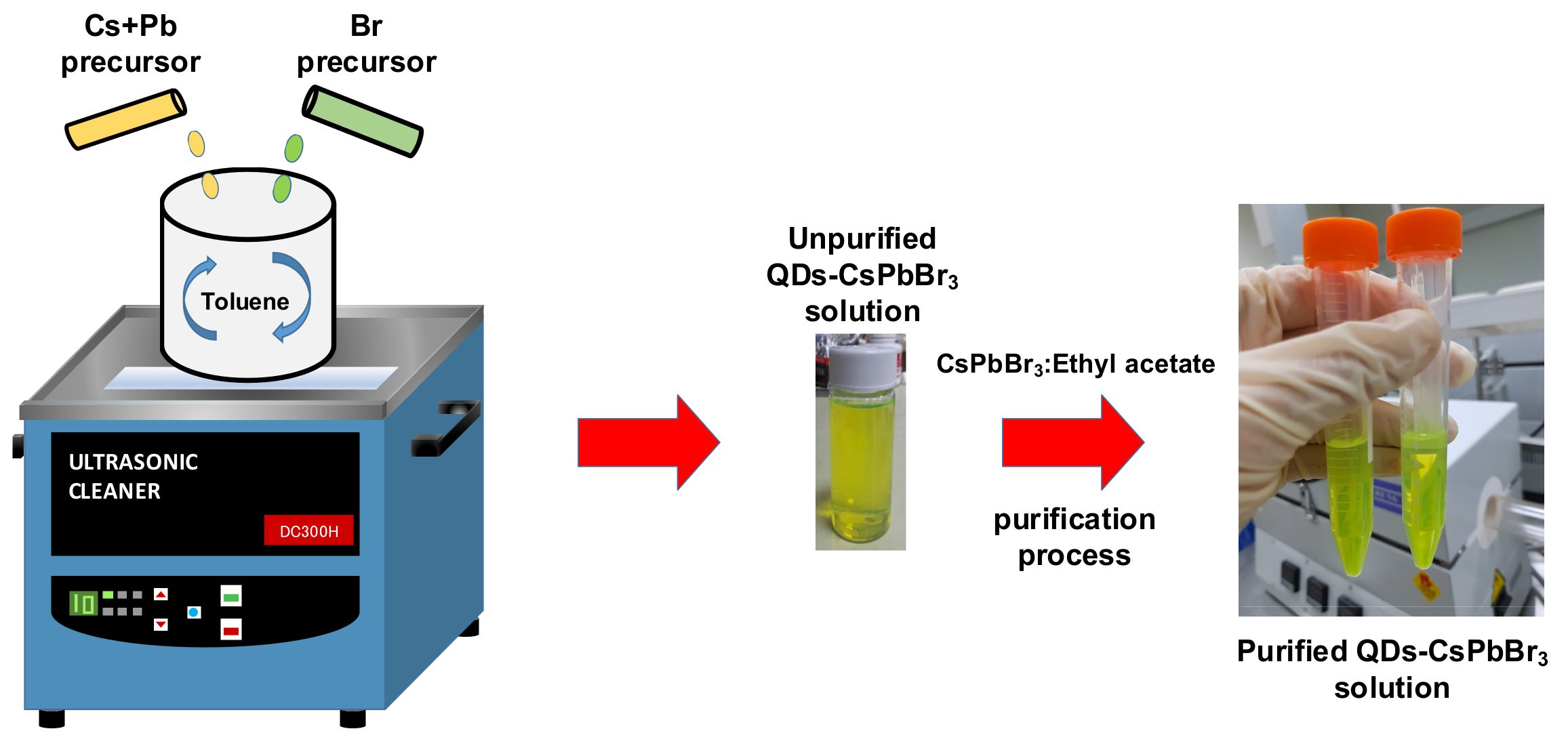
2.1. Synthesis of Perovskite QDs-CsPbBr3 Solution

The synthetic QDs-CsPbBr3 solution in this study was completed by the ultrasonic oscillation method, and its fabrication process steps are shown in Figure 1. The Cs–Pb precursor solutions were prepared by dissolving 0.5 mmol of Cs2CO3 (99.9%, Echo Chemical Co., Ltd., Miaoli, Taiwan) and 1 mmol of PbO (98%, Echo Chemical Co., Ltd., Miaoli, Taiwan), in 5 mL of oleic acid (OA) (99%, Echo Chemical Co. Ltd., Miaoli, Taiwan) solvent into a glass vial. The Cs–Pb precursor solutions were stirred on a hot plate at 160 °C for 30 min until a transparent solution was obtained. Then the glass vial was put in an oven at 120 °C for 30 min to remove the moisture. Then 5 mL of toluene (99%, Echo Chemical Co., Ltd., Miaoli, Taiwan) was added and the Cs–Pb precursor solutions were diluted to 0.1 M. The 0.1 mmol of tetrabutylammonium bromide (TOAB) (98%, Echo Chemical Co. Ltd., Miaoli, Taiwan) were decanted into 0.5 mL of OA and 2 mL of toluene solvents, which were stirred to obtain the Br precursor solutions. The 1 mL of Cs–Pb and all Br precursor solutions were decanted into 15 mL of toluene by an ultrasonic oscillation equipment at an oscillation frequency of 40 KHz for 30 s to form the unpurified QDs-CsPbBr3 solutions. In order to elute the surface ligand of QD, ethyl acetate (99.8%, Echo Chemical Co. Ltd., Miaoli, Taiwan) was used for the purification process. The unpurified QDs-CsPbBr3 solution was added into ethyl acetate with a volume ratio of 1: 3, and then the QDs-CsPbBr3 green precipitates were collected after 10 min of centrifugation at 5000 rpm. Subsequently, the collected green precipitate was stored under vacuum for 12 h to eliminate solvent to accomplish the purification step. The QDs-CsPbBr3 green precipitate was dissolved into 1 mL of hexane (95%, Echo Chemical Co. Ltd., Miaoli, Taiwan), and then vortexed with an ultrasonic oscillator for 5 min to prepare the purified perovskite QDs-CsPbBr3 solution.

2.2. Synthesis of Perovskite QDs-CsPbX3 (X = Cl and I) Solution

For the synthesis of CsPbBr1.5CI1.5 and CsPbBrl2 QD solution additionally, the different volumes of chloroform (99.9%, Echo Chemical Co., Ltd. Miaoli, Taiwan) solution of tetrabutylammonium chloride (TBAC) (98%, Echo Chemical Co., Ltd. Miaoli, Taiwan) (0.02 M) or tetrabutylammonium iodide (TBAI) (98%, Echo Chemical Co. Ltd., Miaoli, Taiwan) (0.2 M) were dropped into the crude colloidal perovskite QDs-CsPbBr3 solution until the desired emission peak position was achieved.

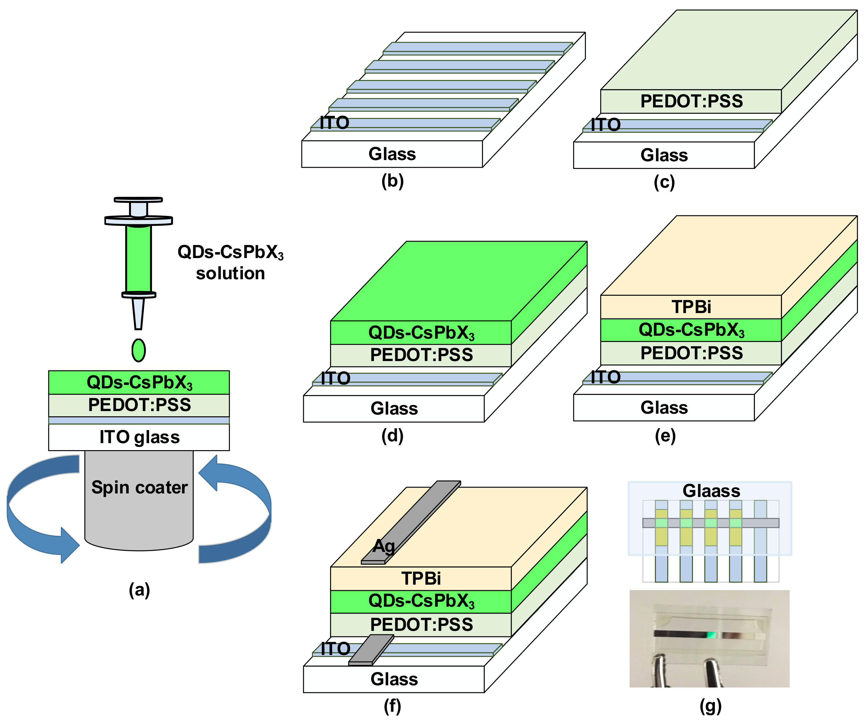
2.3. Fabrication of Perovskite QDs-CsPbX3 LEDs

Figure 2 shows the perovskite QDs-CsPbX3 LED process steps. The patterned ITO-coated glass substrate was sequentially cleaned through acetone, ethanol, and isopropyl alcohol for 30 min. After that, the patterned ITO-coated glass substrate was treated with UV-Ozone cleaning for 20 min to remove the residual organic matter. The PEDOT:PSS solution (UR-AI4083, Uni-Onward Corp., New Taipei City, Taiwan) was deposited onto the patterned ITO-coated glass substrate by spin coating at 4000 rpm for 60 s. The substrate was then annealed at 120 °C for 10 min to form a hole injection layer. The perovskite QDs-CsPbX3 solutions as an active layer was spin-coated on the PEDOT:PSS layer at 1000 rpm for 15 s. Finally, the 40-nm-thick 1,3,5-Tris (1-phenyl-1H-benzimidazol-2-yl) benzene (TPBi) as an electron transport layer and the 100-nm-thick Ag cathode were deposited using a thermal evaporation system at rates of 0.04–0.05 nm/s and 0.22–0.24 nm/s, respectively, under a high vacuum of 1.5 × 10⁻⁶ Torr. The device active area is about 2 mm × 2 mm. After fabrication, the perovskite QDs-CsPbBr3 LEDs were encapsulated in a glove box. Figure 3 shows a cross section scanning electron microscope (SEM) image of the device where the different layers can be identified.

2.4. Characterization

The X-ray diffraction (XRD) patterns measurements were obtained using a CuKα (λ = 1.5418 Å) radiation source operated at 40 kV and 25 mA (X’Pert PRO MRD, PANalytical, Almelo, The Netherlands). The photoluminescence (PL) spectra were measured using a fluorescence spectrophotometer (F-7000, Hitachi, Tokyo, Japan). The PL quantum yield (PLQY) was measured directly using a FluoroMax Horiba spectrofluorometer with an integrating sphere fiber-coupled to a fluorometer (Horiba Jobin Yvon, Longjumeau, France). The nanosecond time-resolved PL decay was analyzed by a commerical optical-microscope-based system (UniRAM, Protrustech, Tainan, Taiwan). For the time-resolved PL measurement, the wavelength, pulse duration, and repetition rate of the excitation were 405 nm, 150 ps, and 20 MHz, respectively. The surface morphology was observed from field emission scanning electron microscope (FESEM) (ZEISS Sigma, ZEISS, Munich, Germany). The perovskite QD size and energy dispersive X-Ray (EDX) spectrum were characterized using transmission electron microscopy (TEM) (JEM-2100F, JEOL, Tokyo, Japan). The current density–voltage–luminance (J–V–L), current efficiency (CE) characteristics, and electroluminescence (EL) spectra of perovskite QDs-CsPbBr3 LEDs were measured using a Keithley 2400 source meter and a spectrascan® spectroradiometer PR-670 (Photo Research Inc., Syracuse, NY, USA) at room temperature.

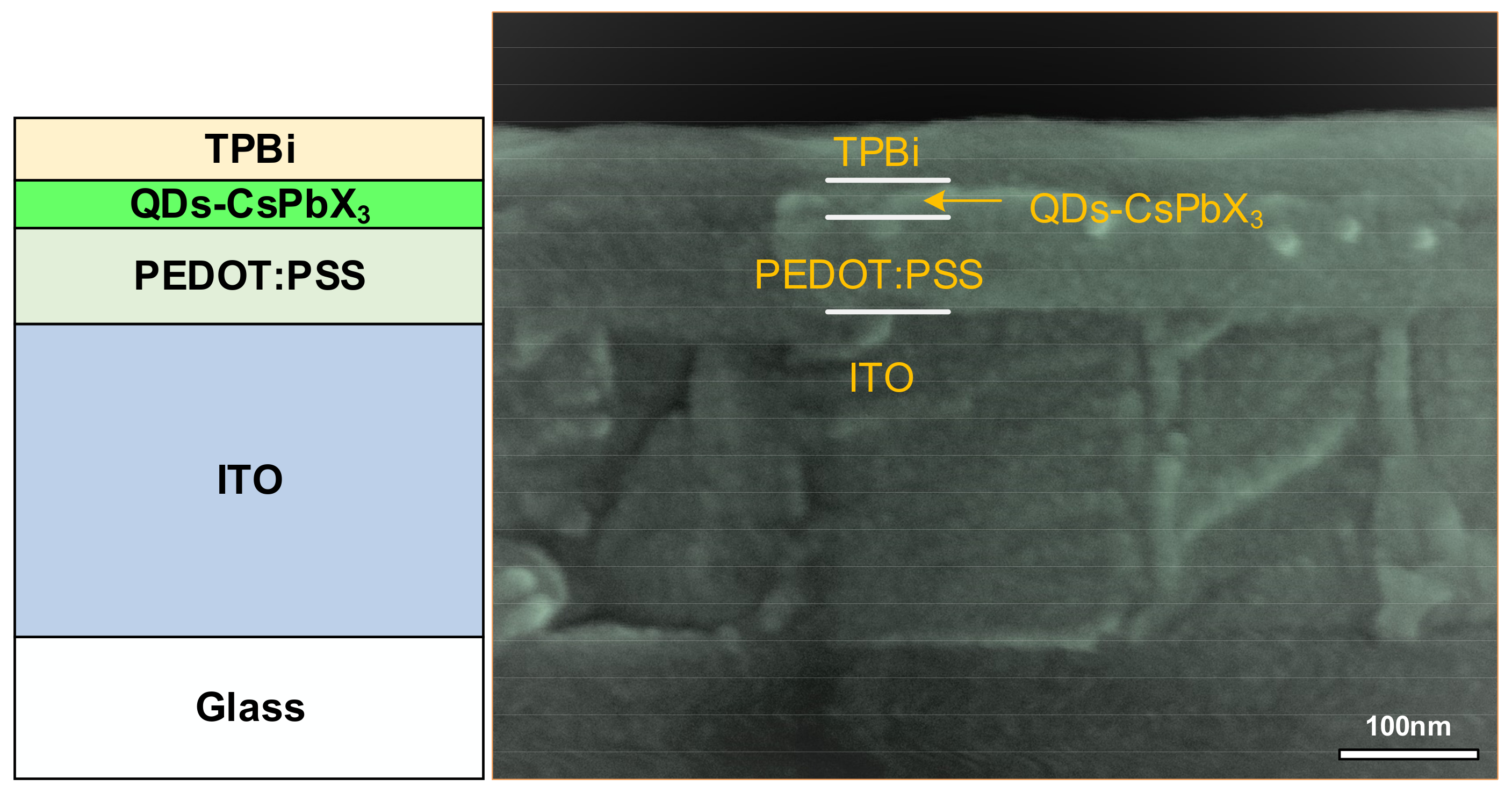
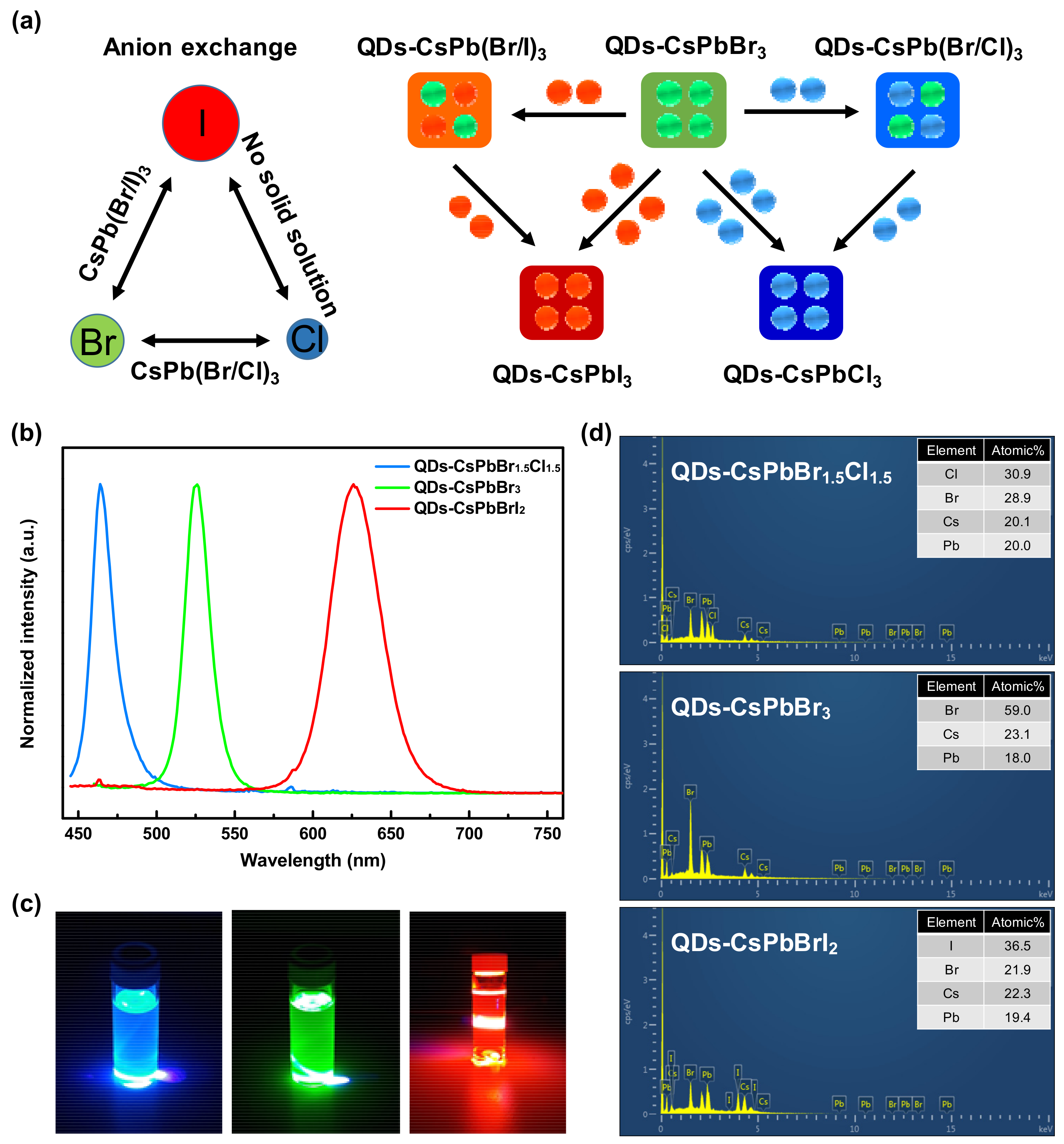
3. Results and Discussion

Because of the significant difference between the Cl and I ion radii, the halogen ion in the perovskite structure is replaced either completely or partially. This exchange process can form CsPb(Cl/Br)3 and CsPb(Br/I)3 systems, but it is impossible to obtain CsPb(Cl/I)3 [4,5,7]. The schematic of the anion exchange between the QDs-CsPbX3 reported in this work is shown in Figure 4a. The emission spectra of colloidal QDs-CsPbX3 (X = Cl, Br, and I) solution (Figure 4b,c) can be adjusted over the entire visible spectral region of 450–650 nm by changing the ratio composition of mixed halide systems (Cl/Br and Br/I) and the particle size. In our work, as TBAC or TBAI was added to the QDs-CsPbBr3 initial solution, respectively, the blue or red shift of the PL peak positions were observed, indicating that Br was gradually replaced by Cl or I to form QDs-CsPbBr1.5Cl1.5 and QDs-CsPbBrI2. The QDs-CsPbBr1.5Cl1.5 exhibited blue emission with PL peak at 464 nm and full width at half maximum (FWHM) = 19 nm; QDs-CsPbBr3 exhibited green emission with PL peak at 524 nm and FWHM = 20 nm; and QDs-CsPbBrI2 exhibited red emission with PL peak at 626 nm and FWHM = 38 nm. The EDX spectrum presented in Figure 4d confirmed that the QDs-CsPbX3 were composed of mainly Cs, Pb, Cl, Br, and I elements. The detailed element ratio of Cs, Pb, and halogen ions are shown in inset of Figure 4d.
Figure 5a shows the synthesized single-or double-halide QDs-CsPbX3 (X = Cl, Br, or I) films XRD patterns. It can be seen that the exchange does not affect the crystal structure of the synthesized QDs-CsPbBr3, and the QDs-CsPbBr3 diffraction peaks gradually shift toward the QDs-CsPbBr1.5Cl1.5 and CsPbBrI2 peaks, inferring that the difference in ionic radius between Cl and I- may be the cause of the diffraction peak shift. As shown in Figure 5b, the unpurified and purified QDs-CsPbBr3 XRD patterns were deposited onto glass substrates. The two dominant diffraction peaks of the unpurified QDs-CsPbBr3 film were (100) at 2θ = 15.384° and (200) at 2θ = 30.823°. In addition, the purified QDs-CsPbBr3 film were (100) at 2θ = 15.334° and (200) at 2θ = 30.823°, respectively. It is clear that QDs-CsPbBr3 does not change the crystal structure characteristics after the purification procedure. According to literature reports [36,37], both Rietveld refinement and pair distribution function (PDF) analyses of X-Ray total scattering data are used to observe that the orthorhombic distortion of the cubic phases does indeed exist when the material is in the form of colloidal nanocrystals. The strong peak with high intensity of the (200) plane of purified QDs-CsPbBr3 indicates that the crystal gave a radial preferential orientation to the (200) crystal plane, along the radial direction, which matches well with the orthorhombic perovskite crystal structure of Pnma (62) space group.
The lattice structure, aggregation situation, and particle size of QDs-CsPbBr3 were observed using TEM. The test sample was prepared using the square mesh copper TEM grids to extract the QDs-CsPbBr3 solution, so that the QDs were uniformly dispersed on the copper mesh to prepare a sample to be observed. All the samples display a narrow size distribution and square shape. Figure 6a,c show TEM images of the unpurified and purified QDs-CsPbBr3, respectively. The size distributions of the unpurified QDs-CsPbBr3 was calculated using ImageJ software (National Institutes of Health, Bethesda, MD, USA) with average diameters of about 16.83 nm. As can be seen from Figure 6c, after QDs-CsPbBr3 solution purification procedure, the purified QDs-CsPbBr3 has significantly narrowed down the size distributions of the QDs with an average diameter of about 13.46 nm. We observed that most of the extra-large, aggregative, and ultra-small QDs were removed after purification. It is more uniform. It was observed that the lattice fringes of the unpurified and purified QDs-CsPbBr3 were 0.31 nm and 0.62 nm (Figure 6b,d), respectively, corresponding to the d-spacing of (200) crystal faces.
Figure 7a,b were SEM images (top-view) of the surface morphology for unpurified and purified QDs-CsPbBr3 coated onto glass substrates. The actual unpurified and purified QDs-CsPbBr3 coated onto glass samples is shown in Figure 7c. It could be observed that the unpurified QDs-CsPbBr3 films were composed of unique shape with different sizes, which has obvious uneven surface morphology because of quantum dot surface defects. On the other hand, the SEM result displays the comparable uniform particle size distribution of the purified QDs-CsPbBr3 films, which probably could be ascribed to the increased crystallinity of the perovskite quantum dots after purification and the quantum dots size grew bigger. It shows that the purification process makes the quantum dots disperse well and less prone to agglomeration. The purified QDs-CsPbBr3 films show highly luminescent and uniform green PL image under UV-365 nm illumination (Figure 7d). Enhanced perovskite QD film PL emission via purification engineering is advantageous to achieve high performance LEDs.
Figure 8a presents normalized PL spectra (excitation wavelength of 365 nm) of unpurified and purified QDs-CsPbBr3 solutions, where narrow PL bandwidths of 20.90 and 20.11 nm as well as emission peaks at 525.6 and 523.8 nm, respectively, can be seen, indicating that QDs-CsPbBr3 possessed good size monodispersity and high nanocrystal quality after the purification process. The bandgap energy of QD increases with the reduction in its size because of quantum confinement. Compared with the unpurified QDs-CsPbBr3, the purified QDs-CsPbBr3 displayed wavelength blue shift and narrow PL bandwidth, indicating that the QD size became larger owing to the aggregation effect and the particle size distribution was more uniform [38]. Meanwhile, PLQYs of unpurified and purified QDs-CsPbBr3 were measured to be 76.6% and 99.2%, respectively, representing a 29.5% enhancement in the quantum yield after purification, as shown in Figure 8b,c. There is a very significant improvement compared to the 50–85% quantum yield of Ref. [5]. It was confirmed that the purification process did increase the quantum yield. We further investigated the time-resolved PL decay of unpurified and purified QDs-CsPbBr3 (Figure 8d). The PL decay curves were fitted to the bi-exponential decay model Y(t), which is described as follows [9]:
Y ( t ) = A 1 exp ( t / τ 1 ) + A 2 exp ( t / τ 2 ) ,
where τ1 and τ2 represent the fast and slow decay time constants, and A1 and A2 represent the amplitudes of the fast and slow components, respectively. The average lifetime was calculated as follows:
τ a v e = A 1 τ 1 2 + A 2 τ 2 2 A 1 τ 1 + A 2 τ 2 ,
The unpurified QDs-CsPbBr3 exhibits an averaged PL lifetime of 20.9 ns, while the purified QDs-CsPbBr3 exhibits an increased PL lifetime of 26 ns. It can be deduced that the non-radiative decay in the purified QDs-CsPbBr3 is suppressed via the purification process, which helps to increase exciton survival time and radioactive recombination probability.
The flat-band energy level of the perovskite QDs-CsPbX3 LED structure was illustrated in Figure 9a, in which PEDOT:PSS and TPBi were used to enhance hole injection and electron transport, respectively. When an electric field is applied, electrons and holes are injected into the perovskite QD layer for radiation recombination. As shown in Figure 9b, perovskite QDs-CsPbX3 LEDs show saturated and color-pure emission, which control the QDs-CsPbX3 bandgap, primarily by tailoring the halide composition, and achieve EL across a wide range of the visible spectrum. The red, green, and blue devices emit at wavelengths of 635, 526, and 478 nm, with QDs-CsPbBr1.5Cl1.5, QDs-CsPbBr3, and QDs-CsPbBrI2 compositions, respectively. All devices exhibit narrow-width emission, with their FWHM in the range of 24–51 nm. Compared to the PL emission peaks of three QDs-CsPbBr1.5Cl1.5, QDs-CsPbBr3, and QDs-CsPbBrI2 solutions, all these EL emission peaks widened and slightly red-shifted, which may be due to solvent influence [39,40], or from the electric-field-induced Stark effect and inter-particle interactions [40,41,42]. Figure 9c–e shows the detailed current density–voltage (J–V), luminance–voltage (LV) and current efficiency–voltage (CE-V) characteristics of QDs-CsPbX3 LEDs. The QDs-CsPbBr1.5Cl1.5, QDs-CsPbBr3, and QDs-CsPbBrI2 devices show diode characteristics and turn-on voltages (defined with a luminance of 1.0 cd/m2) of about 7.0–8.0 V. The increase in luminance is observed with increasing voltage, which attain the maximum values of 1.0, 5.1, and 1.8 cd/m2 achieved in the QDs-CsPbBr1.5Cl1.5, QDs-CsPbBr3, and QDs-CsPbBrI2 devices, respectively, at current densities of 66, 76.9, and 250 mA/cm2. As shown in the inset of Figure 9d, the results confirm that QDs-CsPbX3 LEDs implementation with various colors ranging from red to blue is possible. Uniform red, green, and blue light emerges and emits brightly enough to be obviously seen with human eyes in a regular light environment. The CE roll-off at high current density was also observed for most devices. The QDs-CsPbBr1.5Cl1.5, QDs-CsPbBr3, and QDs-CsPbBrI2 devices presented maximum CEs of 0.002, 0.01, and 0.001 cd/A, respectively, at current densities of 29, 28.3, and 84.6 mA/cm2. Correspondingly, the EQE as a function of voltage characteristic of the QDs-CsPbBr3 LEDs was plotted in Figure 9f. The QDs-CsPbBr1.5Cl1.5, QDs-CsPbBr3, and QDs-CsPbBrI2 devices show the highest EQEs of 0.002, 0.003, and 0.004%, respectively, at brightnesses of 4.5, 8.0, and 6.5 V. The performance metrics for all devices were listed in Table 1.

4. Conclusions

In conclusion, we prepared highly luminescent perovskite QDs-CsPbBr3 solutions using a simple ultrasonic oscillation technique, and demonstrated a purification process for QDs-CsPbBr3 solutions using weakly polar solvents to completely protect the surface ligand of the QDs and remove impurities (reaction solvent and desorbed ligands). After the purification process, the highly luminescent perovskite QDs-CsPbBr3 solutions with a high PLQY of 99.2% and highly bright green emission (526 nm) were obtained. Additionally, QD-CsPbX3 (X = Cl, Br, and I) is modulated using the anion exchange technique. The bright photoluminescence could be adjusted over nearly the whole visible spectral region (450–650 nm). From the TEM and SEM observation, compared with the unpurified QDs-CsPbBr3, the purified QDs-CsPbBr3 has better dispersibility in the solvent and is less prone to agglomeration of QD particles, which is favorable for forming a dense QDs film under spin coating. The as-fabricated highly luminous perovskite QDs-CsPbBr3 films, when applied as the active layer in LEDs, showed a record maximum luminance of 5.1 cd/m2.

Author Contributions

L.-C.C. carried out the experiments and designed the study and gave significant suggestions on writing the whole manuscript. C.-H.T. conceived the original idea and wrote the manuscript. Y.-S.D. and Z.-J.L. prepared the samples and performed all measurements. K.-Y.L. and Z.-L.T. helped to analyze and interpret the data, and helped draft the manuscript. All authors approved this manuscript.

Funding

This research was funded by MOST Nos. 107-2221-E-027-053 and 108-2221-E-131-009-MY2.

Acknowledgments

This work was supported by the by Ministry of Science and Technology (Taiwan, R.O.C.) under Contract Nos. 107-2221-E-027-053 and 108-2221-E-131-009-MY2.

Conflicts of Interest

The authors declare no conflict of interest.

References

  1. Protesescu, L.; Yakunin, S.; Bodnarchuk, M.I.; Krieg, F.; Caputo, R.; Hendon, C.H.; Yang, R.X.; Walsh, A.; Kovalenko, M.V. Nanocrystals of cesium lead halide perovskites (CsPbX3, X = Cl, Br, and I): Novel optoelectronic materials showing bright emission with wide color gamut. Nano Lett. 2015, 15, 3692–3696. [Google Scholar] [CrossRef]
  2. Pan, A.; He, B.; Fan, X.; Liu, Z.; Urban, J.J.; Alivisatos, A.P.; He, L.; Liu, Y. Insight into the ligand-mediated synthesis of colloidal CsPbBr3 perovskite nanocrystals: The role of organic acid, base, and cesium precursors. ACS Nano 2016, 10, 7943–7954. [Google Scholar] [CrossRef] [PubMed]
  3. Zhang, M.; Tian, Z.Q.; Zhu, D.L.; He, H.; Guo, S.W.; Chen, Z.L.; Pang, D.W. Stable CsPbBr3 perovskite quantum dots with high fluorescence quantum yields. New J. Chem. 2018, 42, 9496–9500. [Google Scholar] [CrossRef]
  4. Nedelcu, G.; Protesescu, L.; Yakunin, S.; Bodnarchuk, M.I.; Grotevent, M.J.; Kovalenko, M.V. Fast anion-exchange in highly luminescent nanocrystals of cesium lead halide perovskites (CsPbX3, X = Cl, Br, I). Nano Lett. 2015, 15, 5635–5640. [Google Scholar] [CrossRef] [PubMed]
  5. Wei, S.; Yang, Y.C.; Kang, X.J.; Wang, L.; Huang, L.J.; Pan, D.C. Room-temperature and gram-scale synthesis of CsPbX3 (X = Cl, Br, I) perovskite nanocrystals with 50–85% photoluminescence quantum yields. Chem. Commun. 2016, 52, 7265–7268. [Google Scholar] [CrossRef] [PubMed]
  6. Li, X.; Wu, Y.; Zhang, S.; Cai, B.; Gu, Y.; Song, J.; Zeng, H. Quantum Dots: CsPbX3 quantum dots for lighting and displays: Room-temperature synthesis, photoluminescence superiorities, underlying origins and white light-emitting diodes. Adv. Funct. Mater. 2016, 26, 2435–2445. [Google Scholar] [CrossRef]
  7. Akkerman, Q.A.; D’Innocenzo, V.; Accornero, S.; Scarpellini, A.; Petrozza, A.; Prato, M.; Manna, L. Tuning the optical properties of cesium lead halide perovskite nanocrystals by anion exchange reactions. J. Am. Chem. Soc. 2015, 137, 10276–10281. [Google Scholar] [CrossRef]
  8. Swarnkar, A.; Chulliyil, R.; Ravi, V.K.; Irfanullah, M.; Chowdhury, A.; Nag, A. Colloidal CsPbBr3 perovskite nanocrystals: Luminescence beyond traditional quantum dots. Angew. Chem. Int. Ed. 2015, 54, 15424–15428. [Google Scholar] [CrossRef]
  9. Du, X.F.; Wu, G.; Cheng, J.; Dang, H.; Ma, K.Z.; Zhang, Y.W.; Tan, P.F.; Chen, S. High-quality CsPbBr3 perovskite nanocrystals for quantum dot light-emitting diodes. RSC Adv. 2017, 7, 10391–10396. [Google Scholar] [CrossRef]
  10. Veldhuis, S.A.; Ng, Y.F.; Ahmad, R.; Bruno, A.; Jamaludin, N.F.; Damodaran, B.; Mathews, N.; Mhaisalkar, S.G. Crown ethers enable room-temperature synthesis of CsPbBr3 quantum dots for light-emitting diodes. ACS Energy Lett. 2018, 3, 526–531. [Google Scholar] [CrossRef]
  11. Dong, Y.; Gu, Y.; Zou, Y.; Song, J.; Xu, L.; Li, J.; Xue, J.; Li, X.; Zeng, H. Improving all-inorganic perovskite photodetectors by preferred orientation and plasmonic effect. Small 2016, 12, 5622–5632. [Google Scholar] [CrossRef] [PubMed]
  12. Li, Y.; Shi, Z.F.; Li, S.; Lei, L.Z.; Ji, H.F.; Wu, D.; Xu, T.T.; Tian, Y.T.; Li, X.J. High-performance perovskite photodetectors based on solution-processed all-inorganic CsPbBr3 thin films. J. Mater. Chem. C 2017, 5, 8355–8360. [Google Scholar] [CrossRef]
  13. Liu, C.; Hu, M.; Zhou, X.; Wu, J.; Zhang, L.; Kong, W.; Li, X.; Zhao, X.; Dai, S.; Xu, B.; et al. Efficiency and stability enhancement of perovskite solar cells by introducing CsPbI3 quantum dots as an interface engineering layer. NPG Asia Mater. 2018, 10, 552–561. [Google Scholar] [CrossRef]
  14. Yuan, H.; Zhao, Y.; Duan, J.; Wang, Y.; Yang, X.; Tang, Q. All-inorganic CsPbBr3 perovskite solar cell with 10.26% efficiency by spectra engineering. J. Mater. Chem. A 2018, 6, 24324–24329. [Google Scholar] [CrossRef]
  15. Huang, C.Y.; Zou, C.; Mao, C.; Corp, K.L.; Yao, Y.C.; Lee, Y.J.; Schlenker, C.W.; Jen, A.K.Y.; Lin, L.Y. CsPbBr3 perovskite quantum dot vertical cavity lasers with low threshold and high stability. ACS Photonics 2017, 4, 2281–2289. [Google Scholar] [CrossRef]
  16. Li, J.; Dong, H.; Xu, B.; Zhang, S.; Cai, Z.; Wang, J.; Zhang, L. CsPbBr3 perovskite quantum dots: Saturable absorption properties and passively Q-switched visible lasers. Photonics Res. 2017, 5, 457–460. [Google Scholar] [CrossRef]
  17. Xie, Y.; Yu, Y.; Gong, J.; Yang, C.; Zeng, P.; Dong, Y.; Yang, B.; Liang, R.; Ou, Q.; Zhang, S. Encapsulated room-temperature synthesized CsPbX3 perovskite quantum dots with high stability and wide color gamut for display. Opt. Mater. Express 2018, 8, 3494–3505. [Google Scholar] [CrossRef]
  18. Wang, C.M.; Su, Y.M.; Shih, T.A.; Chen, G.Y.; Chen, Y.Z.; Lu, C.W.; Yu, I.S.; Yang, Z.P.; Su, H.C. Achieving highly saturated single-color and high color-rendering-index white light-emitting electrochemical cells by CsPbX3 perovskite color conversion layers. J. Mater. Chem. C 2018, 6, 12808–12813. [Google Scholar] [CrossRef]
  19. Guhrenz, C.; Benad, A.; Ziegler, C.; Haubold, D.; Gaponik, N.; Eychmüller, A. Solid-state anion exchange reactions for color tuning of CsPbX3 perovskite nanocrystals. Chem. Mater. 2016, 28, 9033–9040. [Google Scholar] [CrossRef]
  20. Tan, Z.K.; Moghaddam, R.S.; Lai, M.L.; Docampo, P.; Higler, R.; Deschler, F.; Price, M.; Sadhanala, A.; Pazos, L.M.; Credgington, D.; et al. Bright light-emitting diodes based on organometal halide perovskite. Nat. Nanotechnol. 2014, 9, 687–692. [Google Scholar] [CrossRef]
  21. Yu, J.C.; Kim, D.B.; Baek, G.; Lee, B.R.; Jung, E.D.; Lee, S.; Chu, J.H.; Lee, D.K.; Choi, K.J.; Cho, S.; et al. High-performance planar perovskite optoelectronic devices: A morphological and interfacial control by polar solvent treatment. Adv. Mater. 2015, 27, 3492–3500. [Google Scholar] [CrossRef] [PubMed]
  22. Cho, H.; Jeong, S.H.; Park, M.H.; Kim, Y.H.; Wolf, C.; Lee, C.L.; Heo, J.H.; Sadhanala, A.; Myoung, N.; Yoo, S.; et al. Overcoming the electroluminescence efficiency limitations of perovskite light-emitting diodes. Science 2015, 350, 1222–1225. [Google Scholar] [CrossRef] [PubMed]
  23. Deng, W.; Xu, X.; Zhang, X.; Zhang, Y.; Jin, X.; Wang, L.; Lee, S.T.; Jie, J. Organometal halide perovskite quantum dot light-emitting diodes. Adv. Funct. Mater. 2016, 26, 4797–4802. [Google Scholar] [CrossRef]
  24. Lee, J.W.; Choi, Y.J.; Yang, J.M.; Ham, S.; Jeon, S.K.; Lee, J.Y.; Song, Y.H.; Ji, E.K.; Yoon, D.H.; Seo, S.; et al. In-situ formed type I nanocrystalline perovskite film for highly efficient light-emitting diode. ACS Nano 2017, 11, 3311–3319. [Google Scholar] [CrossRef] [PubMed]
  25. Lee, S.; Park, J.H.; Lee, B.R.; Jung, E.D.; Yu, J.C.; Nuzzo, D.D.; Friend, R.H.; Song, M.H. Amine-based passivating materials for enhanced optical properties and performance of organic inorganic perovskites in light-emitting diodes. J. Phys. Chem. Lett. 2017, 8, 1784–1792. [Google Scholar] [CrossRef] [PubMed]
  26. Chen, L.C.; Lee, K.L.; Wu, W.T.; Hsu, C.F.; Tseng, Z.L.; Sun, X.H.; Kao, Y.T. Effect of different CH3NH3PbI3 morphologies on photovoltaic properties of perovskite solar cells. Nanoscale Res. Lett. 2018, 13, 140. [Google Scholar] [CrossRef]
  27. Chen, L.C.; Lin, Y.S.; Tang, P.W.; Tai, C.Y.; Tseng, Z.L.; Lin, J.H.; Chen, S.H.; Kuo, H.C. Unraveling current hysteresis effects in regular-type C60-CH3NH3PbI3 heterojunction solar cells. Nanoscale 2017, 9, 17802–17806. [Google Scholar] [CrossRef] [PubMed]
  28. Lee, K.Y.; Chen, L.C.; Wu, Y.J. Effect of oblique-angle sputtered ITO electrode in MAPbI3 perovskite solar cell structures. Nanoscale Res. Lett. 2017, 12, 556. [Google Scholar] [CrossRef]
  29. Chen, L.C.; Weng, C.Y. Optoelectronic properties of MAPbI3 perovskite/titanium dioxide heterostructures on porous silicon substrates for cyan sensor applications. Nanoscale Res. Lett. 2015, 10, 404. [Google Scholar] [CrossRef]
  30. Song, J.; Li, J.; Li, X.; Xu, L.; Dong, Y.; Zeng, H. Quantum dot light-emitting diodes based on inorganic perovskite cesium lead halides (CsPbX3). Adv. Mater. 2015, 27, 7162–7167. [Google Scholar] [CrossRef]
  31. Pan, J.; Quan, L.N.; Zhao, Y.; Peng, W.; Murali, B.; Sarmah, S.P.; Sinatra, M.Y.L.; Alyami, N.M.; Liu, J.; Yassitepe, E.; et al. Highly efficient perovskite-quantum-dot light-emitting diodes by surface engineering. Adv. Mater. 2016, 28, 8718–8725. [Google Scholar] [CrossRef] [PubMed]
  32. Li, J.; Xu, L.; Wang, T.; Song, J.; Chen, J.; Xue, J.; Dong, Y.; Cai, B.; Shan, Q.; Han, B.; et al. 50-fold EQE improvement up to 6.27% of solution-processed all-inorganic perovskite CsPbBr3 QLEDs via surface ligand density control. Adv. Mater. 2017, 29, 1603885. [Google Scholar] [CrossRef] [PubMed]
  33. Chiba, T.; Hoshi, K.; Pu, Y.J.; Takeda, Y.; Hayashi, Y.; Ohisa, S.; Kawata, S.; Kido, J. High-efficiency perovskite quantum-dot light-emitting devices by effective washing process and interfacial energy level alignment. ACS Appl. Mater. Interfaces 2017, 9, 18054–18060. [Google Scholar] [CrossRef] [PubMed]
  34. Krieg, F.; Ochsenbein, S.T.; Yakunin, S.; Brinck, S.T.; Aellen, P.; Suess, A.; Clerc, B.; Guggisberg, D.; Nazarenko, O.; Shynkarenko, Y.; et al. Colloidal CsPbX3 (X = CI, Br, I) nanocrystals 2.0: Zwitterionic capping ligands for improved durability and stability. ACS Energy Lett. 2018, 3, 641–646. [Google Scholar] [CrossRef] [PubMed]
  35. Tan, Y.; Zou, Y.T.; Wu, L.Z.; Huang, Q.; Yang, D.; Chen, M.; Ban, M.Y.; Wu, C.; Wu, T.; Bai, S.; et al. Highly luminescent and stable perovskite nanocrystals with octylphosphonic acid as a ligand for efficient light-emitting diodes. ACS Appl. Mater. Interfaces 2018, 10, 3784–3792. [Google Scholar] [CrossRef] [PubMed]
  36. Cottingham, P.; Brutchey, R.L. On the crystal structure of colloidally prepared CsPbBr3 quantum dots. Chem. Commun. 2016, 52, 5246–5249. [Google Scholar] [CrossRef] [PubMed]
  37. Bertolotti, F.; Protesescu, L.; Kovalenko, M.V.; Yakunin, S.; Cervellino, A.; Billinge, S.J.L.; Terban, M.W.; Pedersen, J.S.; Masciocchi, N.; Guagliardi, A. Coherent nanotwins and disorder in cesium lead halide perovskite nanocrystals. ACS Nano 2017, 11, 3819–3831. [Google Scholar] [CrossRef] [PubMed]
  38. Li, Z.C.; Kong, L.; Huang, S.Q.; Li, L. Highly luminescent and ultrastable CsPbBr3 perovskite quantum dots incorporated into a silica/alumina monolith. Angew. Chem. 2017, 56, 8134–8138. [Google Scholar] [CrossRef]
  39. Sun, Q.; Wang, Y.A.; Li, L.S.; Wang, D.; Zhu, T.; Xu, J.; Yang, C.; Li, Y. Bright, multicoloured light-emitting diodes based on quantum dots. Nat. Photonics 2007, 1, 717–722. [Google Scholar] [CrossRef]
  40. Zhao, J.; Bardecker, J.A.; Munro, A.M.; Liu, M.S.; Niu, Y.; Ding, I.K.; Luo, J.; Chen, B.; Jen, A.K.; Ginger, D.S. Efficient CdSe/CdS quantum dot light-emitting diodes using a thermally polymerized hole transport layer. Nano Lett. 2006, 6, 463–467. [Google Scholar] [CrossRef]
  41. Empedocles, S.A.; Bawendi, M.G. Quantum-confined stark effect in single CdSe nanocrystallite quantum dots. Science 1997, 278, 2114–2117. [Google Scholar] [CrossRef] [PubMed]
  42. Xu, W.; Ji, W.; Jing, P.; Yuan, X.; Wang, Y.A.; Xiang, W.D.; Zhao, J.L. Efficient inverted quantum-dot light-emitting devices with TiO2/ZnO bilayer as the electron contact layer. Opt. Lett. 2014, 39, 426–429. [Google Scholar] [CrossRef] [PubMed]
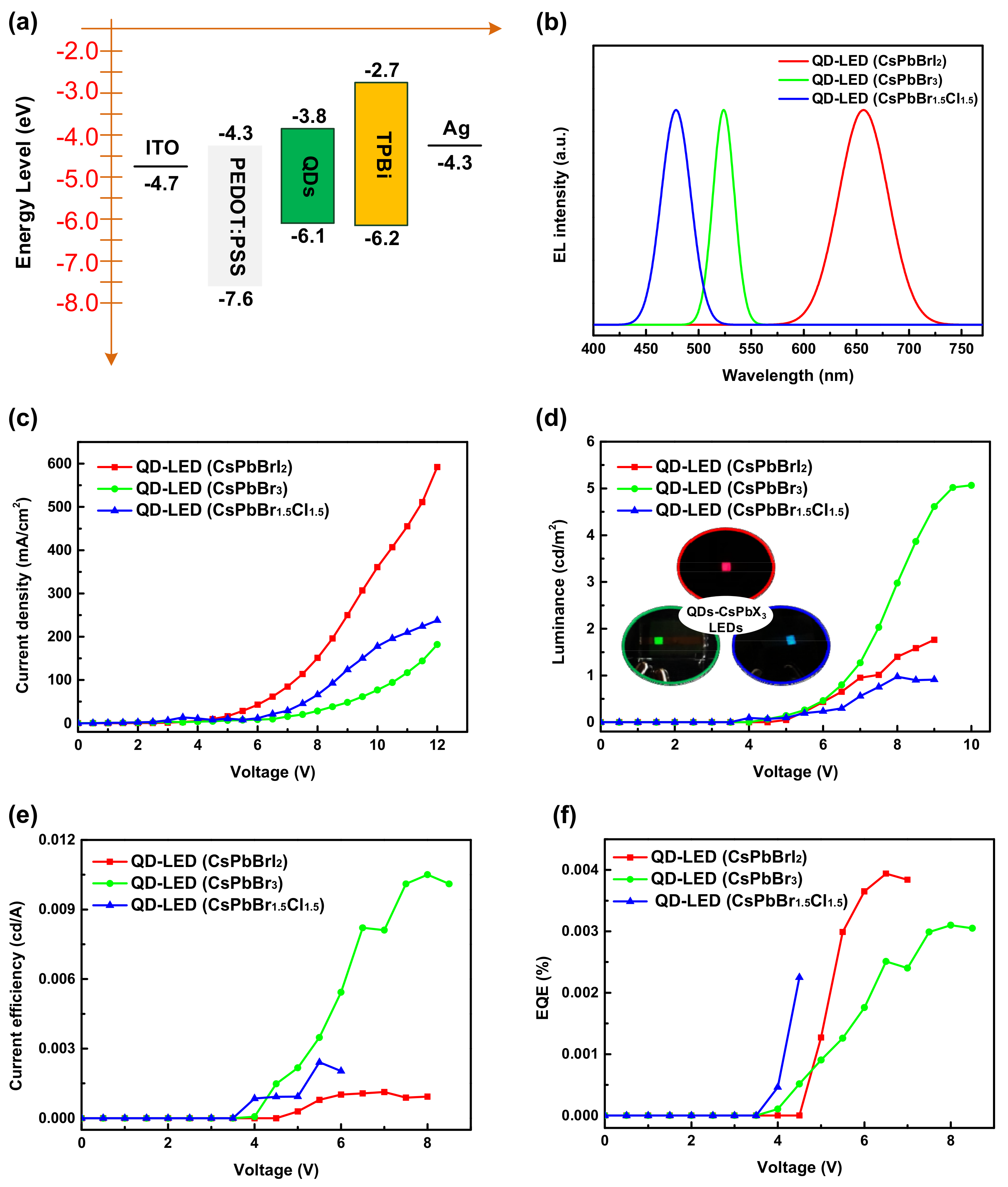
Figure 1. Perovskite quantum dots (QDs)-CsPbBr3 solution fabrication process steps.
Energies 12 03507 g001
Figure 2. Perovskite QDs-CsPbX3 light-emitting diode (LED) process steps. (a) QDs-LED device spin-coating process schematic diagram; (b) Patterned ITO-coated glass; (c) PEDOT:PSS hole injection layer preparation; (d) QDs-CsPbX3 active layer preparation; (e) 1,3,5-Tris(1-phenyl-1H-benzimidazol-2-yl) benzene (TPBi) electron transport layer deposition; (f) Ag electrode deposition; (g) Original QDs-LED device picture.
Energies 12 03507 g002
Figure 3. Device architecture and cross-sectional scanning electron microscope (SEM) image of the QDs-CsPbX3 LED device.
Energies 12 03507 g003
Figure 4. (a) Schematic of the anion exchange between the QDs-CsPbX3; (b) photoluminescence (PL) emission spectra of QDs-CsPbX3 solutions; (c) the emission photographs of the QDs-CsPbX3 solutions under UV-405 nm laser excitation; (d) energy dispersive X-ray (EDX) analysis for the purified QDs-CsPbX3.
Energies 12 03507 g004
Figure 5. X-ray diffraction (XRD) patterns of (a) single-or double-halide QDs-CsPbX3 films; (b) unpurified and purified QDs-CsPbBr3 films.
Energies 12 03507 g005
Figure 6. Transmission electron microscopy (TEM) images and insert are the size distribution analysis of (a) and (b) unpurified QDs-CsPbBr3, (c) and (d) purified QDs-CsPbBr3.
Energies 12 03507 g006
Figure 7. Top-view SEM images of (a) unpurified QDs-CsPbBr3; (b) purified QDs-CsPbBr3 covered onto glass substrates; (c) unpurified and purified QDs-CsPbBr3-coated glass films; and (d) highly luminescent purified QDs-CsPbBr3 films (λ = 365 nm).
Energies 12 03507 g007
Figure 8. (a) Normalized PL emission spectra of unpurified and purified QDs-CsPbBr3 solutions; (b) and (c) photoluminescence quantum yield (PLQYs) of unpurified and purified QDs-CsPbBr3 solutions; (d) Time-Resolved Photoluminescence (TRPL) decay profiles of unpurified and purified QDs-CsPbBr3 solutions.
Energies 12 03507 g008
Figure 9. Perovskite QDs-CsPbBr3 LED device performance: (a) Flat-band energy-level diagram of QDs-CsPbBr3 LEDs; (b) Electroluminescence (EL) spectra of QDs-CsPbX3 LED devices; (c) J–V characteristic; (d) LV characteristic and the photographs showing various color emissions from the perovskite QDs-CsPbX3 LEDs in operation (inset); (e) CEV characteristic; (f) EQE-V characteristic.
Energies 12 03507 g009
Table 1. Summary of perovskite QDs-CsPbX3 LEDs performance.
PerovskiteColorEL Peak (nm)FWHM (nm)Lmax (cd/m2)CEmax (cd/A)EQEmax (%)
QDs-CsPbBrI2Red635511.80.0010.004
QDs-CsPbBr3Green526245.10.010.003
QDs-CsPbBr1.5Cl1.5Blue478331.00.0020.002

