Advances in La-Based High-k Dielectrics for MOS Applications

1
Department of Electrical and Electronic Engineering, The University of Hong Kong, Hong Kong 999077, China
2
Bio-inspired Sensors and Optoelectronics Laboratory (BISOL), EECS, Northwestern University, Evanston, IL 60208, USA
3
Department of Applied Physics, The Hong Kong Polytechnic University, Hong Kong 999077, China
*
Authors to whom correspondence should be addressed.
Coatings 2019, 9(4), 217; https://doi.org/10.3390/coatings9040217
Submission received: 3 March 2019
/
Revised: 20 March 2019
/
Accepted: 25 March 2019
/
Published: 27 March 2019
(This article belongs to the Special Issue Metal-Semiconductor and Insulator-Semiconductor Interfaces)
Abstract
:This paper reviews the studies on La-based high-k dielectrics for metal-oxide-semiconductor (MOS) applications in recent years. According to the analyses of the physical and chemical characteristics of La2O3, its hygroscopicity and defects (oxygen vacancies, oxygen interstitials, interface states, and grain boundary states) are the main problems for high-performance devices. Reports show that post-deposition treatments (high temperature, laser), nitrogen incorporation and doping by other high-k material are capable of solving these problems. On the other hand, doping La into other high-k oxides can effectively passivate their oxygen vacancies and improve the threshold voltages of relevant MOS devices, thus improving the device performance. Investigations on MOS devices including non-volatile memory, MOS field-effect transistor, thin-film transistor, and novel devices (FinFET and nanowire-based transistor) suggest that La-based high-k dielectrics have high potential to fulfill the high-performance requirements in future MOS applications.
1. Introduction
As the complementary metal-oxide-semiconductor (CMOS) technology is continually approaching the giga-scale in terms of integration level, the MOS devices have to be scaled to the nano-scale. According to the roadmap on the development of the semiconductor industry, the key geometric parameters for several technology nodes calculated by the technology rules are listed in Table 1 [1]. However, the minimum thickness of SiO2 as a gate dielectric is ~0.7 nm because at least two layers of neighboring oxygen atoms are needed to prevent the gate/SiO2 and SiO2/Si interfaces from overlapping with each other [2]. However, practically, for SiO2 dielectrics thinner than 3 nm, the gate leakage is too large for applications because direct tunneling of charge carriers occurs [3,4]. Figure 1a is an example of gate leakage increasing significantly with the decrease of dielectric thickness [5], where for a 1.5 nm oxide film, the unacceptable gate leakage exceeds 100 A/cm2 at 2 V. Figure 1b shows the factors that contribute to the gate leakage current of MOS devices, including Fowler-Nordheim tunneling [6], Poole-Frenkel tunneling [7,8], trap-assisted tunneling [9,10], and direct tunneling [11]. Among them, direct tunneling has the closest relation with the thickness of the gate dielectric, and its current can be calculated as:
where J0 is a constant, Vox is the voltage drop of the dielectric, ΦB is the barrier height, m* is the electron effective mass in the dielectric, ℏ is the reduced Planck’s constant, and Tox is the dielectric thickness. Obviously, the direct tunneling current increases exponentially with the decrease of Tox. Therefore, the replacement of SiO2 by an alternative material with higher dielectric constant (k) allows the use of larger physical thickness for the same oxide capacitance, and so the tunneling current can be suppressed.
The first high-k material studied is silicon oxynitrde (SiOxNy). By annealing in NH3 or other gases containing nitrogen (N), effective N incorporation is achieved in SiO2 to improve its thermal and high-field reliability [12]. Besides, reports show that N doping is capable of reducing oxide charges and border traps [13]. However, SiOxNy could no longer meet the requirement of gate leakage during scaling down in the ITRS report in 2007, and so novel high-k materials as gate dielectrics had to be explored. According to Figure 2, that demonstrates the dielectric constants of promising candidates for MOS devices together with their band gaps and conduction-band offsets (CBO) with Si and GaAs [14,15], inverse trends in the variations of Eg and CBO with the k value can be found. Therefore, in order to reach a balance in this trade-off, apart from possessing a high k value, sufficiently large Eg (usually > 5 eV) and CBO with the substrate (usually > 1 eV) to minimize carrier injection should also be required. Besides, thermal stability is an additional criterion for choosing proper high-k dielectrics: large Gibbs free energy to inhibit the reaction with the Si substrate and small oxygen diffusion coefficient to suppress the formation of low-k SiOx interfacial layer during high-temperature processing steps are essential [16,17].
Through comprehensive consideration of the pertinent requirements for high-k gate dielectrics, following SiOxNy, hafnium (Hf)-based materials attracted much attention and were successfully introduced into production in 2007, with the TEM images of a PMOS transistor and its MOS gate stack shown in Figure 3 [18]. However, owing to lower thermal stability and lower interface quality with Si than SiO2, HfO2 is still far from being ideal. Therefore, measures including post-deposition annealing (PDA) and nitrogen incorporating and doping of Si, Al, La, etc. to form ternary oxides have been tried with good results achieved [19]. In the past decade, much efforts have been made to study novel high-k dielectrics in a variety of semiconductor devices, and hundreds of reports have shown the high potential of high-k gate dielectrics for application in the CMOS and VLSI technologies. For example, Al2O3, ZrO2, Ta2O5, and Al-doped TiO2 have been proved to be promising candidates for DRAM. Hf- and Zr-based ternary oxides have been widely used in MOSFET, FinFET, etc. [20]. Recently, flexible and stretchable electronics has become a hotspot for applications such as flexible displays, wearable sensors and electronic skins. Therefore, massive studies have been made on thin-film transistors (TFTs) with flexible/stretchable substrates. At the beginning, Al2O3 was proved to be an excellent gate dielectric for TFT [21]. However, its low k value limits its further applications. So, research interests moved to composite/stack layers involving materials with higher k values such as Ga2O3, Hf-/Zr-based ternary oxides/oxynitrides, rare-earth oxides, and perovskites [22]. Speaking of perovskites, their super-high k value (300~6000) makes them stand out in high-k dielectrics, among which SrTiO3 and BaTiO3 are the most representative dielectric perovskite oxides. However, the phase of perovskite is critical because most perovskite oxides are insulators in the cubic phase while variation in crystallinity induces metallic, superconducting, ferroelectric, and ferromagnetic properties [23]. Therefore, the deposition of perovskite oxides as dielectrics in MOS applications is the main issue. Then, the idea of using perovskite nanocrystals or nanocomposites has been proposed. Firstly, self-assembled BaTiO3 and (Ba, Sr)TiO3 nanocrystals have been tried on pentacene TFT with a mobility of 0.35 cm2·V−1·s−1 [24]. Synthesized BaTiO3 has also been studied with a k value of 4000 achieved [25]. Moreover, a study on BaTiO3/polypropylene nanocomposites showed a rubber shell of nano-scaled BaTiO3 could promote the compatibility and dispersion of nano-particles in polypropylene matrix and also improve the dielectric and tensile properties of nanocomposites [26]. However, the uncertainty in the phase of perovskite oxide is still limiting the performance of relevant MOS devices.
Then, rare-earth oxide as a high-k dielectric has been studied, and La2O3 is a representative that has attracted much attention in recent years due to its high k value (~27) [27], large band gap (5.8~6.0 eV) [28], high breakdown field (> 13 MV/cm) [29], low leakage current for small effective oxide thickness (EOT) [30], good thermodynamic stability, and good high-field reliability on Si [30,31]. Based on the WKB approximation, the direct tunneling currents of ideal MOS structures with different dielectrics were modeled and simulated by H. Wu, et al., with results demonstrated in Figure 4 [32]. Significant gate leakage decrease is achieved by replacing SiO2 with high-k materials, among which La2O3 has the lowest leakage current. Besides, unlike perovskites, high-quality La2O3 film can be easily deposited by sputtering, ALD, PVD, E-beam, etc. These make La-based high-k materials highly promising for MOS applications.
However, besides the crystallization temperature (~500 °C) of La2O3 [19] not being high enough for high-temperature processing during fabrication, its hygroscopicity and defects [31,33] are the main concerns for MOS applications. Therefore, similar to HfO2, treatments including nitrogen incorporation and metal doping are necessary for La2O3 to improve its oxide quality. So, based on the advantages of La2O3 over other high-k materials and with the motivation of providing guidelines for making good use of La-based high-k materials to improve the performance of MOS devices for meeting the requirements of the technology nodes in the future, this review focuses on the advances of La-based high-k dielectrics in MOS applications. To have a better understanding of the characteristics of the La-based films; the basic theories for the main concerns of La2O3 as gate dielectric and the proposed solutions to these problems are discussed in Section 2, including the hygroscopicity of La2O3, the defects in La2O3, and the mechanisms for the effects of La in La-based ternary oxides. Then, the advances of the MOS applications with La-based high-k dielectrics are reviewed in Section 3 to provide a whole picture on the developments and advantages of La-based high-k dielectrics in MOS devices. The applications in Section 3 include non-volatile memory, MOSFET, TFT, Ge and III-V compound semiconductor devices, and novel MOS devices (e.g. FinFETs and nanowire FETs) because these are the main devices that need high-k dielectrics for high-performance MOS applications in the future. At last, a brief conclusion is made in Section 4 based on the discussions in Section 2 and Section 3, and future studies are proposed to give directions to the developments of MOS devices with La-based high-k dielectrics.
2. Characteristics of La-Based High-k Dielectrics
2.1. Hygroscopicity of La2O3
As mentioned above, theoretically, the k value of La2O3 is ~27, but lower k values, even below 10, were found in early studies [34,35,36]. One important reason is the hygroscopic nature of La2O3, whose high ionicity leads to a direct reaction with H2O:
Experimental results [37] showed that after exposure to air for 12 h, the root-mean-squared (RMS) surface roughness of La2O3 increased from 0.5 to 2.4 nm (Figure 5a), which was probably caused by the non-uniform moisture absorption of the La2O3 film that led to a non-uniform volume expansion. Apart from the surface roughness, increases in physical thickness and thus capacitor equivalent thickness (CET) occurred as shown in Figure 5b which should be ascribed to the lower density of hexagonal La(OH)3 (4.445 g/cm3) than that of hexagonal La2O3 (6.565 g/cm3). The obvious increase of CET resulted in a significant degradation in k value from 20 to 7 (Figure 5b). Besides, this moisture absorption further affected the electrical properties of MOS devices. Figure 5c demonstrates that the flat-band voltage (Vfb) shift and hysteresis of an MOS capacitor with La2O3 gate dielectric increase with exposure time, implying that negative charges and traps are induced near/at the La2O3/Si interface [38].
A lot of effort has been made to enhance the hygroscopic resistance of La2O3 so that its advantages as a gate dielectric can be made use of. The most widely used method is incorporating a second metal element to form a ternary oxide. The rate of the reaction between a metal oxide (MxOy) and moisture (H2O) can be evaluated by the Gibbs free energy change (ΔG) [39]. A negative ΔG means the system energy decreases after the reaction, implying that the reaction has a high possibility to occur, and so a more positive ΔG is more promising for the corresponding high-k material to suppress the hygroscopicity of La2O3 [37,40]. For example, in Ref. [37], Y incorporation exhibited obvious improvement in the moisture resistance of La2O3, as shown in the inset of Figure 6, where for Y concentration higher than 40%, the degradation in k value after exposure in air is negligible. Apart from the materials in Figure 6, Ta and Nb have also been proved to be promising dopants to improve the hygroscopic resistance of La2O3 by surface morphology and XPS analysis, which showed that the La–OH peak significantly decreased with increasing Ta and Nb contents in TaLaO [41] and NbLaO [42], respectively.
Another method is post-deposition ultraviolet (UV) ozone treatment using an Hg vapor UV lamp that primarily emits light with wavelengths of 185 and 254 nm [43]. The UV ozone treatment is compared with thermal N2 and O2 treatments in Figure 7. Obviously, the O2 + N2 annealing can inhibit the moisture absorption of La2O3 by a large extent, but the N2 annealing together with the UV ozone treatment keeps the La2O3 surface roughness almost unchanged after exposing to air for 24 h.
2.2. Defects in La2O3
Although high-k dielectrics can keep the trend of device scaling, their higher density of bulk defects and poorer interface with Si than SiO2 results in degradation in carrier mobility, thus making the device performance unsatisfactory [44,45,46]. As shown in Figure 8a, fixed charge, oxide trap, interface trap, interfacial dipole, and surface roughness are the factors that lead to Coulomb, phonon and surface-roughness scatterings (in Figure 8b), which govern the effective carrier mobility of MOS devices at low, moderate and high gate fields respectively. The origins of these scatterings are: Firstly, the defects in high-k oxide bulk cause charge trapping and lead to higher bias instability and unreliability [47]; secondly, optical phonons in high-k oxides have a low-lying soft polar mode which results in the remote scattering of channel carriers [48]. Besides, the larger surface roughnesses of high-k dielectrics with both the Si substrate and the gate than those of SiO2 should be ascribed to the interaction between high-k elements with the Si substrate and the longer metal–O and metal-Si bonds than the Si–Si bond.
Since the reliability issues of gate dielectric film (including mobility degradation, threshold-voltage shift, and biased temperature instability) are mainly governed by the neutral and charged defects located in the dielectric film and at the dielectric/substrate interface, it is necessary to explore the characteristics of these defects. Oxygen-related defects are the dominant point defects in binary high-k oxides, mainly including oxygen vacancy and oxygen interstitial. Unlike HfO2 with only four-fold O sites, hexagonal La2O3 has two different types of oxygen vacancies (VO), with four-fold and six-fold coordination, respectively. The energy levels of VO in La2O3 are demonstrated in Figure 9a [49], obtained by the first-principle calculations based on the total energy plane wave pseudopotential code CASTEP [50], with the band structure of La2O3 with neutral VO shown in Figure 9b as an example [51]. Four-fold VO has all five charged states including 2−, 1−, 0, 1+, and 2+. However, since high coordination prevents distortion from creating an extra gap state, the six-fold VO only consists of 0, 1+, and 2+ states. Obviously in Figure 9a, all the VO states in La2O3 are located above the band gap of Si, which differs from the case of HfO2. The neutral VO state in HfO2 is below the conduction band of Si [52], and so can be filled by the electrons injected from the silicon substrate, leading to a positive shift in the capacitance-voltage (C–V) curve [53]. J. X. Zheng, et al. calculated the concentrations of VO and oxygen interstitial (Oi) in La2O3 based on the density functional theory in the generalized gradient approximation using the projector augmented wave method, with results shown in Figure 9c [54]. For HfO2, the concentrations of positively-charged oxygen vacancy and negatively-charged oxygen interstitial are too low (<1012 cm−3) to significantly affect the device performance. However, for La2O3, the concentrations of VO2+ and Oi2− are higher than 1016 cm−3, and so, apart from neutral VO, charged VO and Oi can also be the sources of charge trapping.
Trap at the La2O3/semiconductor interface is another concern that impacts the device performance. La has been reported to easily react with semiconductor substrates such as Si and Ge to form a low-k interfacial layer (IL). As illustrated in Figure 10a, the thickness of the IL can be comparable to the thickness of the La2O3 bulk, which significantly decreases the effective k value of the dielectric and thus increases the EOT [55,56]. As shown in Figure 10d, post-deposition annealing can enhance this reaction because an obvious increase in the La-silicate peak can be found for higher annealing temperature [57]. However, a tradeoff exists between the k value and the interface-trap density (Dit), according to Ref. [56]. As the thickness of the IL (with a k value of 5.8) increases from 0.7 to 3.0 nm, Dit decreases by almost two orders but the effective k value of the dielectric is reduced by ~70%. With a La-silicate IL, the interface states are depicted in Figure 10b [58]. It is known that La2O3 has an ionic bonding nature while the bond in the La-silicate layer is more covalent, thus creating a larger amount of oxygen vacancies at the La2O3/Si interface [59]. It has been reported that charge-pumping measurement can be used to detect the interface traps between ionic HfO2 and covalent SiO2, and so the traps located at the La2O3/La-silicate interface can be considered as slow states [60]. Figure 10c shows the density of this slow state (Dslow) together with Dit calculated based on the measured conductance of the La2O3-gated MOS capacitor, with Dslow much higher than Dit and almost distributed uniformly in the Si band gap [58].
Besides, the grain-boundary state created by the crystallization of high-k material during high-temperature treatments is another kind of defect that induces shallow traps. Figure 10e shows the XRD patterns of La2O3 and LaON after annealing, and the weaker peak of LaON than that of La2O3 indicates that nitrogen incorporation can suppress the crystallization of La2O3 [61]. Apart from increasing the crystallization temperature, N incorporation is also capable of increasing the k value and reducing the border traps in the dielectric [62]. For many years, in order to decrease the defect density of the La2O3 gate dielectric, many efforts have been made, including high-temperature annealing, N incorporation, F or NH3 treatment, doping other high-k metal elements to form complex oxides (e.g. LaYO [37], LaTaO [41]), and addition of an interfacial passivation layer (e.g., Al2O3 [27]). However, because of the trade-off between the k value and the dielectric/semiconductor interface quality, there is still ample room to improve the device performance
2.3. Effects of La on La-doped Ternary Oxides
As mentioned in the previous section, doping other high-k metal elements into La2O3 is capable of enhancing the device performance. It has been reported that doping La into other high-k materials can also achieve improvements, and the most important effect of La doping is to passivate the oxygen vacancies in other high-k binary oxides. After several reports showing that La incorporated in HfO2 could significantly improve the device performance [53,54,55,56,57,58,59,60,61,62,63,64,65,66], X. P. Wang et al. proposed that this improvement should be ascribed to the reduction of oxygen vacancies (VO) in HfLaO [66]. Therefore, several studies on the physics of this phenomenon have been made and confirmed the VO passivation role of La as discussed below.
The relaxed structures of VO in HfO2 and HfLaO were obtained by first-principle calculation based on the density-functional theory using a generalized gradient approximation (Figure 11a) [67], according to which the formation energies of VO near La and far from La were calculated to be 6.29 and 5.73 eV respectively, both larger than the VO formation energy of HfO2 (5.58 eV), indicating that it is more difficult to form VO’s after La incorporation. The reason for this increased VO formation energy by La incorporation can be explained by Figure 11b, with the contour plots for the wave functions corresponding to the VO-related states. Although electrons are trapped in VO in both HfO2 and HfLaO cases, the electron distribution around VO of HfO2 differs from that of HfLaO. Since the La–O bond is 76% ionic and higher than Hf–O (70%) according to the Pauling’s electronegativity theory, electrons from the O2p states are localized at the O sites beside the La atoms, thus reducing the interaction between La5d and O2p when compared to that between Hf5d and O2p. Therefore in Figure 11b, unlike in HfO2, the oxygen atom nearest to La atoms does not contribute to the gap state at all [67]. Moreover, D. Liu et al analyzed the band structures of HfO2 and HfLaO with VO’s and concluded that La was capable of passivating VO’s in HfO2 and ZrO2 by shifting the vacancy gap into the conduction band, thus suppressing the Fermi-level pinning at the dielectric/Si interface as shown in Figure 11c [68]. In the case of pure HfO2, oxygen tends to diffuse to the Si substrate and leaves a positive VO by releasing two electrons that fall down to the Fermi level of the metal gate. However, if a thin La2O3 layer lies on the HfO2 dielectric, La can easily diffuse into HfO2 under high-temperature annealing [69] and then the substitution of Hf by La creates holes in the valence band (VB). Therefore, in this case, the oxidation of Si drives this substitution without releasing electrons, and the VB holes are filled by the electrons in the conduction band to prevent the formation of VO states in the band gap.
Apart from oxygen-vacancy passivation, La incorporation has also been reported to be able to modify the flatband voltage (VFB) of the gate stack in nFETs [69,70] and so shift their threshold voltages (Vth). An obvious negative shift of VFB for HfLaO-gated MOS capacitor with increasing La concentration can be found in Figure 12a, and the effective work function (EWF) decreases by about 0.5 eV for the La content rising from 20% to 60% [71]. Recently, the EWF shift due to La incorporation into HfO2 has been found to be linearly dependent on the La concentration, with −53 meV per 1014 atoms/cm2 [72]. This should be ascribed to the formation of a dipole layer at the HfLaO/SiO2 interface as shown in the inset of Figure 12b and the VFB shift can be calculated by:
where Q is the areal charge density in the dipole layer, d1 and d2 are the widths of dipole layers on the SiO2 and HfLaO sides, kSiO2 and kHfLaO are the k values of SiO2 and HfLaO, and x is the thickness of the HfLaO layer. Since an offset can be caused by the dipole layer inside the dielectric film and is independent of the dipole position, the VFB shift almost remains constant as the CET varies (Figure 12a).
An interface dipole moment model has been proposed by P. D. Kirsch et al. through a study of Vth shift for nFETs with rare-earth element (La, Sr, Er, and Sc)-doped HfO2 [73]. Similarly, the dipole vector formed by incorporating rare-earth oxides could induce a shift in EWF, resulting in the Vth tuning of MOS devices. According to the experimental results, Vth approximately varied proportionally and inversely proportionally with the electronegativity and ionic radius of the dopant respectively. This is consistent with the conclusion drawn by L. Lin et al. that it is the dopant electronegativity that influenced the magnitude of the interfacial dipole moment and thus ΔVFB [74]. Moreover, the physical origin for the formation of the dipole layer has been ascribed to the difference in areal density of oxygen atoms (σ) between the oxides [75]. The formation process of the dipole layer is shown in Figure 12d, in which σHK and σSiO2 are the areal densities of oxygen atoms in high-k oxide and SiO2 respectively. For the case that σHK is smaller than σSiO2, in order to relax the structure, an oxygen atom tends to move towards the high-k side, thus resulting in the formation of a dipole consisting of a negatively-charged center in the high-k oxide and a positively-charged oxygen vacancy nearby.
3. Applications of La-based High-k Gate Dielectrics
3.1. Nonvolatile Memory
As the nonvolatile memory evolves from ROM (read-only memory) to flash memory, new materials, new structures and new operating principles have been continually explored in order to break the limitation that the electrons stored in the floating gate significantly decrease during the scaling down of floating-gate flash memory [76]. The new structures of flash memory include ferro-electric random-access memory (FeRAM), nanoelectromechanical memory (NEMM), magneto-resistive random-access memory (MRAM), phase-change memory (PCM), and charge-trapping memory (CTM). Although CTM introduced in 1967 is the oldest, its high storage density, simple fabrication and compatibility with the CMOS technology make it a promising candidate for the next-generation flash memory technology [77]. Nowadays, the structure of CTM is based on a metal gate/oxide blocking layer (BL)/nitride charge trapping layer (CTL)/oxide tunneling layer (TL) gate stack on nm Si substrate as shown in Figure 13a. P-type Si is more often used than n-type Si because the electrons in the n-type channel formed at the surface of a p-type substrate have higher mobility than the holes in the p-type channel formed at the surface of an n-type substrate. Whether the CTL stores electrons or not is the way to define ‘1’ and ‘0’ respectively. The TL is formed by an insulating material, which allows electron tunneling from the substrate to the CTL under a positive gate bias and prevents electrons from escaping from the CTL to the substrate under no gate bias. The BL is also formed by an insulating material, which can prevent the electron transfer between the CTL and the gate electrode. Positive or negative voltage is applied to the gate electrode for programming or erasing operation, during which the electric field inside the gate stack enables electrons to flow into or out of the CTL via the TL. In order to further scale down the device, high-k materials such as the BL, CTL and TL have been widely studied, among which La-based high-k materials have been reported to achieve good results as discussed below.
Firstly, when considering replacing SiO2 by high-k material as the BL, apart from the k value, requirements including (i) large band gap and band offset with respect to the CTL, (ii) low density of traps at the interface or in the dielectric bulk, (iii) thermal and kinetic stability, and (iv) compatibility with the CMOS technology, should be fulfilled. According to Figure 13b, with an ideal high-k BL, the electric field across the tunneling layer can be enhanced, thus improving the program/erase (P/E) speed [78]. Owing to a large band gap (8.8 eV) and good stability, Al2O3 has become the best choice for BL, but its low k value (~9) limits the device scaling. Therefore, La-doped Al2O3 (LaAlOx) has been studied for higher k value, and results showed that not only the program speed and Vth window increased, but the retention performance also improved [79]. The LaAlOx layer was deposited by ALD using La(iPrCp)3, Al(CH3)3 and H2O precursors and the atomic ratio of La/(La + Al) was 55%. Compared with Al2O3, LaAlOx as BL brought 40% and 32% improvements in program speed and Vth saturation window, better robustness to voltage stress, and better retention performance below 120 °C. Besides, HfLaO has also been applied as BL and exhibited improvements in Vth saturation window and robustness to voltage stress due to its higher k value (~22) compared to Al2O3. However, the retention performance degraded after La incorporation, probably due to decreased conduction-band offset [79,80].
Secondly, for the TL, a tradeoff exists between high P/E speed and good retention property, and so based on the investigation of the band-engineered barrier, the idea of multi-TL consisting of low-k and high-k dielectrics has been proposed. In Figure 13c, the LaAlO3/SiO2 double TL permits faster P/E because the ΔEc and ΔEv at the LaAlO3/SiO2 interface can give easier electron and hole tunnelings. Moreover, the added LaAlO3 layer increases EOT, and so improves retention [81]. These were confirmed by experimental results: With the addition of the LaAlO3 layer, the memory window measured at ± 16 V for 100 μs increased from 3.3 to 5.6 V, and at 150 °C, an initial ΔVth of 5.6 V and a 10-year window of 3.8 V were achieved for the same P/E voltage and P/E time.
Moreover, La-based high-k materials have been widely investigated as the CTL due to the high k value and deep-level traps of La2O3 [53]. However, since the density of deep-level traps in La2O3 is not high enough, the memory window of the CTM with La2O3 as CTL was only 0.5 V at ± 16 V for 1 s [82]. The main methods to solve this problem are: (i) nitrogen incorporation, which has been reported to induce traps in the bandgap and also remove shallow traps along the grain boundaries in CTLs [83]; (ii) doping other high-k material (e.g. Nb2O5, TiO2), which is another way to increase the deep-level trap density in La2O3 and suppress its reaction with the SiO2 TL as well [84]; (iii) multi-CTL for band engineering, which is capable of enhancing charge-trapping efficiency [85] and improving device reliability by suppressing the impact of TL degradation [86]. Experimentally, these methods have all been studied, and the results in Figure 14 [61,84,87,88,89,90] show obvious improvements in the performance of the memory device. HfLaO nanocrystal can provide the largest memory window, but the 50% degradation after 10 years in the retention property is not good for real applications. Comprehensively speaking, NbLaON is the most promising candidate so far due to its relatively large memory window, good P/E transient characteristics and negligible degradation after 10 years.
3.2. Metal-oxide-semiconductor Field-effect Transistors (MOSFETs)
Having been the basic device of ICs, MOSFET’s with high-k dielectrics have attracted a lot of efforts for more than 20 years. For the gate dielectric, the most important thing is to keep the carrier flow in the channel when biases are applied to the device. So, a sufficiently-large band gap and conduction-band (CB) offset with the channel material are necessary to prevent the current flow from the substrate to the gate. Moreover, the qualities of the dielectric film and the dielectric/substrate interface are also critical because as discussed in Section 2.2 (Figure 8), fixed charges, oxide traps, interface traps, interfacial dipoles, and surface roughness are the factors that lead to carrier scatterings and thus decreased carrier mobility. Therefore, it is important to explore different high-k materials and different post-deposition treatments in order to improve the device performance. Although HfO2 has already been commercially dominant, La2O3 still holds its potential for future generations due to its larger CB offset with the Si substrate than its HfO2 counterpart. As mentioned in Section 2.2, a La-silicate interfacial layer (IL) tends to be formed after high-temperature annealing, which is good for the interface quality but increases the EOT. K. Kakushima et al. have studied the properties of MOSFET with La2O3 as a gate dielectric, in which the La2O3 film was deposited by electron beam evaporation at 300 °C on a p-Si (100) wafer [91]. After a 500 °C rapid thermal annealing (RTA) in forming gas (N2:H2 = 97:3), a 1.57 nm silicate IL was formed in the 3-nm dielectric, leading to an EOT increase from 0.48 to 1.15 nm. However, the mobility peak increased from 60 to 300 cm2/Vs at room temperature and the subthreshold swing (SS) decreased from 120 to 66 mV/dec, which are impressive numbers for MOSFET.
Owing to the hygroscopicity of La2O3 as mentioned in Section 2.1, it is La-based complex oxides that are preferred because of the inevitable exposure to the air or low-vacuum environment. In 2003, LaAlO3 was chosen as the gate oxide for future technology nodes in the semiconductor roadmap [92]. As a perovskite, LaAlO3 has a relatively large band gap (5.6 eV), large CB offset (1.8 eV), small lattice mismatch to Si (1.3%), and small oxygen diffusion coefficient, which are all desirable for epitaxial gate dielectric on Si [93,94,95]. Si MOSFET with LaAlO3 gate dielectric has been reported by I. Y. Chang, et al., where a 7.3-nm LaAlO3 film was deposited on p-Si by RF sputtering and a post-deposition annealing was performed at 700 °C for 30 s in N2 [96]. Results showed that the maximum effective mobility (μeff) at 300 K was 212.6 cm2/Vs; SS was 69.4 mV/dec; and hysteresis was 8.6 mV. According to the analysis on the mechanisms that caused mobility degradation, the Coulomb scattering was roughly the same for LaAlO3 and SiO2-gated MOSFETs, indicating that LaAlO3 is indeed a promising candidate. N incorporation into LaAlO3 has been proved to improve the device properties, including EOT, gate leakage, SS, and drive current [97]. Moreover, HfLaO, LaTiO, LaZrO, LaYO, etc. have all been tried as the gate dielectric for MOSFETs, and the device properties are listed in Table 2 [91,96,98,99,100,101,102]. The carrier mobility of the La2O3/LaSiO sample could reach 300 cm2/Vs, but its EOT was not small enough for further scaling down due to the low k value of SiO2. The LaTiO sample was a good choice because of its high mobility (300 cm2/Vs), small EOT (0.63 nm) and low Vth (0.12 V). However, both the deposition method and post-deposition treatment are different for the dielectrics in Table 2, thus making a fair comparison among the samples difficult. However, all these results demonstrate the high potential of La-based high-k oxides as the gate dielectric of MOSFET.
LaLuO3 with high k value (~30) and low leakage current has also attracted much attention and has been investigated in SOI-MOSFETs [103,104]. E. D. Ozhen, et al. first deposited it on an SOI (100) wafer by molecular beam deposition at 450 °C with a thickness of 6 nm, and a PDA was performed at 400 °C in oxygen and forming gas (H2:N2 = 1:9) sequentially for 10 min each [103]. According to the experimental results, the Vth and SS of the SOI nFET and pFET were 0.22 V and −0.8 V, 72 mV/dec and 65 mV/dec, respectively. The LaLuO3 film exhibited an EOT of 1.55 nm, low Dit of 4.5 × 1011 cm−2·eV−1, and the electron and hole mobilities on the SOI are similar to those of devices based on HfO2 and HfSiON gate dielectrics with a similar EOT. However, the interface and bulk traps of the dielectric might cause a high level of 1/f noise, which could not meet the stricter requirements of the RF and analogue mixed-signal CMOS technologies. Therefore, M. Olyaei, et al. analyzed the low-frequency noise of the SOI-MOSFET with LaLuO3 gate dielectric98. The normalized drain-current noise (SID/ID2) can be calculated by [105]:
where W and L are the width and length of the channel, λ is the tunneling attenuation distance, Nt is the volumetric oxide trap density, Cox is the gate-oxide capacitance, gm is the transconductance, α is the scattering parameter, and γ is the characteristic exponent. The calculation results showed that the LaLuO3-gated device exhibited one to two orders of magnitude higher low-frequency noise than the standard MOSFETs, which is comparable to the devices with Hf-based dielectrics, implying that LaLuO3 is a suitable candidate for balancing the tradeoff between device performance and device scaling.
3.3. Thin-film Transistors (TFTs)
TFT is a field-effect transistor operating as a voltage-controlled current source, and its conducting channel is formed in a thin film of semiconductor (<100 nm). When a bias is applied to the gate, carriers are accumulated at the interface between the gate dielectric and the thin-film semiconductor, thus forming a conducting layer as the channel. With an electric field along this channel generated by an applied drain-source bias, a drain current is created. Similar to the traditional MOSFET theory, the charges and traps in the gate dielectric and at the dielectric/semiconductor interface can influence the carrier mobility and threshold voltage, and so it is also important to improve the qualities of the high-k dielectric and the interface. For the development of TFT in a large-area flat-panel display with high resolution, the requirements cannot be satisfied by conventional Si as the channel material due to the low carrier mobility of amorphous Si and the non-uniform spatial distribution of grain structure in poly-Si. Oxide semiconductor as a channel material for TFT was proposed and studied at the beginning. ZnO TFTs were intensively studied from 2003 due to its high Hall mobility (~200 cm2/Vs). Also, La-based high-k dielectrics were investigated, and especially a recent report proposed a solution-process method for LaAlO3 deposition (spray pyrolysis) without the need for a vacuum environment to produce a TFT with μeff of 12 cm2/Vs, Ion/Ioff ratio of 106 and SS of 650 mV/dec [106]. Unfortunately, the deposited ZnO film was polycrystalline and so suffered from grain-boundary problems, leading to inadequate carrier mobility. After that, amorphous oxide semiconductor started to attract attention, and materials including ZnInSnO, ZnSnO, GaZnSnO, HfInZnO, and InZnO have all been investigated for TFT applications [107,108,109,110,111]. However, considering all the requirements of TFT (e.g. carrier mobility, thermal stability, controllability of carrier concentration, compatibility with current processing techniques), InGaZnO (IGZO) has become the most promising channel material.
First reported in late 2004 [112], IGZO TFT has been applied for mass production and sales since 2013, and adopted in high-end electronic products including iPad Pro and Surface Pro. Also, owing to the problems of scaling down, studies have been made on the use of high-k dielectric for IGZO TFT, especially focusing on La-based high-k materials in recent years. HfLaO was the first La-based high-k dielectric investigated for IGZO TFT in 2009 and achieved low Vth (0.22 V), small SS (76 mV/dec), high carrier mobility (25 cm2/Vs), and large Ion/Ioff ratio (5 × 10⁷), which was the best performance among devices with other high-k gate dielectrics (e.g. Y2O3, Si3N4, AlTiO) [113]. However, there is still much room for improvement. Therefore, different annealing ambients for HfLaO film were then studied with results showing that N2 was a better annealing ambient than O2 and NH3 and the carrier mobility could reach 35 cm2/Vs [114]. After that, more La-based ternary oxides have been studied with good results obtained. The characteristics of IGZO TFTs with promising La-based dielectrics are listed in Table 3 according to recent investigations [42,114,115,116,117], in which ZrLaO provided the highest carrier mobility (67.2 cm2/Vs) but lower high-field reliability, while LaAlO3 was able to achieve low operating voltage (0.29 V) and small SS (98 mV/dec) but low mobility (5.4 cm2/Vs). Comprehensively speaking, NbLaO is the best candidate due to relatively high mobility (28.0 cm2/Vs), relatively low Vth (1.84 V), high on/off ratio (3.6 × 10⁷), and negligible hysteresis (0.07 V).
As the large-area flat-panel display is developing for flexible applications nowadays, the idea of applying organic semiconductors as channel material has been proposed. Among the organic semiconductors, only a few have been reported to produce TFT’s with a carrier mobility higher than 1 cm2/Vs, namely 6T, dinaphtho [2, 3-b:29, 39-f] thieno [3, 2-b] thiophene (DNTT), and pentacene, with pentacene showing the greatest potential. Similarly, investigations of a pentacene-based organic thin-film transistor (OTFT) with La-based high-k dielectrics in recent years have achieved impressive device performances. C. Y. Han, et al. studied La incorporation into Y2O3, ZrO2, and Nb2O5 for pentacene OTFT applications, and results showed that La incorporated in ZrO2 and Nb2O5 significantly reduced their traps, thus increasing the carrier mobility [118]. The carrier mobilities of ZrLaO- and NbLaO-gated OTFTs were 70 times and 300 times those of their counterparts based on ZrO2 and Nb2O5 respectively. However, the trap density in Y2O3 was increased by the La doping, leading to a degradation in carrier mobility. From another perspective, with Zr, Nb or Y added in La2O3, the moisture absorption of La2O3 could be suppressed, and so larger pentacene grains were grown on the smoother oxide surface (Figure 15a), thus resulting in higher carrier mobility. Table 4 lists the device properties of pentacene OTFT’s with La-based ternary oxides as gate dielectrics [41,118,119,120,121,122], with both NbLaO and TaLaO providing carrier mobility higher than 1 cm2/Vs. Similar to IGZO TFT, NbLaO can also achieve high performance for OTFT (high carrier mobility and high on/off ratio), which indicates its high potential in the applications of flexible electronics.
For flexible applications, pentacene OTFTs with La-based dielectrics have been tried on flexible substrates recently. M. F. Chang et al. reported pentacene OTFT on flexible polyimide (PI) (Kapton HPP-ST, Dupont) with HfLaO as a gate dielectric (Figure 15b) [123]. The device structure is depicted in the inset of Figure 15c: a 30 nm HfLaO dielectric was deposited on a TaN gate, followed by an O2 treatment for 30 min at 200 °C, and Au was used as the source/drain electrodes. According to the transfer characteristics in Figure 15c, the carrier mobility, SS, Vth, and Ion/Ioff ratio were extracted to be 0.13 cm2/Vs, 130 mV/dec, −1.25 V, and 1.2 × 10⁴ respectively, which can be useful for flexible electronics. Recently, vacuum tape has been reported to be the substrate of pentacene OTFT with NbLaO as a gate dielectric (Figure 15d) [124]. With the device structure shown in the inset of Figure 15e, Al electrode was first evaporated on vacuum tape as a gate electrode; then an 80 nm NbLaO film was deposited by RF sputtering; a PDA was performed in N2 for 20 min at 200 °C; and Au was thermally evaporated as the source/drain electrodes. Similarly, the transfer characteristics in Figure 15e are used for parameter extraction, and the the carrier mobility, SS, Vth, and Ion/Ioff ratio are 4.8 cm2/Vs, 174 mV/dec, −1.90 V, and 4.52 × 10⁴ respectively, which are impressive. Especially, the carrier mobility in this work is higher than most previously reported on OTFT’s with flexible substrates, and is comparable to the highest (9.5 cm2/Vs) up till now [125].
3.4. Ge and III-V Metal-oxide-semiconductor (MOS) Devices
In order to further increase the drive current of transistors to meet the requirements in the future, semiconductors with higher carrier mobility have been investigated to replace Si for a few decades. The replacement began with strained Si and SiGe, but limitations were found in mobility degradation and Vth shift. The next step was using Ge due to its superior intrinsic electron mobility (3900 cm2/Vs) and hole mobility (1900 cm2/Vs). Unfortunately, the insufficiently oxidized interfacial layer (GeOx) with high Dit could significantly deteriorate the performance of Ge MOS devices, and so the studies in recent years mainly focused on the passivation of the Ge surface for lower Dit.
Rare-earth oxides (e.g. CeO2, Dy2O3, Gd2O3 and La2O3) have been suggested for passivating the oxide/Ge interface. Especially for La2O3, a stable La-germanate interlayer can be formed as mentioned in Section 2.2 (Figure 10a), and is capable of inhibiting the volatilization of the GeO sub-oxides at the Ge surface, thus suppressing the formation of interfacial defects [126]. O. Bethge et al. reported the characteristics of an Au-Ti alloy/ZrO2/La2O3/Ge gate stack, in which La2O3 was the interfacial passivation layer (IPL) (1 nm) and ZrO2 was the gate dielectric (6.5 nm), both deposited by ALD [127]. The PDA was in Ar for 5 min at 350 °C and the post-metallization annealing (PMA) was performed in forming gas (H2:N2 = 1:9) for 30 min also at 350 °C. The extracted k value of the dielectric stack was promising (14.7), but the Dit at midgap of 1.2 × 1012 cm−2·ev−1 was still not low enough. After that, nitrogen incorporation during the deposition of La2O3 by RF sputtering has been studied [128]. In order to suppress the moisture absorption of LaON, a 1-nm Al2O3 was deposited also by sputtering for covering purposes. Conditions for the PDA and PMA were 500 °C in N2 for 5 min and 300 °C in forming gas (H2:N2 = 5:95) for 20 min respectively. Obvious improvements after nitrogen incorporation were obtained and LaON achieved a low Dit with the Ge substrate (4.96 × 1011 cm−2·ev−1). Moreover, La-based ternary oxides and dual passivation layers have been investigated with good results available, and the characteristics of Ge MOS devices with La-based dielectrics and/or passivation layers reported recently are summarized in Table 5 [56,127,128,129,130,131,132].
The ZrO2/La2O3 dielectric stack has been applied by W. B. Chen et al. in Ge n-MOSFET with a laser annealing (LA) treatment to increase its gate capacitance density [133]. The 5-nm high-k IPL and dielectric stack were deposited by PVD, followed by a PDA in O2. Then, the LA was performed in the air with laser spot sizes of 0.3 cm2 (after focus) and 0.9 cm2 (without focus) for n+/p junction and high-k dielectric respectively and was stepped continuously in the x and y directions until the whole sample was covered. Results showed that with the LA treatment, Cox rose from 1.8 μF/cm2 to 2.7 μF/cm2, thus decreasing the EOT from 1.6 to 0.95 nm. Besides, good transistor characteristics including high carrier mobility (μeff, peak ~600 cm2/Vs), small SS (106 mV/dec) and low Vth (0.18 V) were obtained.
Compared with Ge, III–V compound semiconductors own even higher electron mobility and so have become promising candidates for Si replacement. Among all the III–V compounds, GaAs with five times higher electron mobility and larger band gap (1.42 eV) than Si has attracted the most attention in recent years, especially in MOS devices with high-k gate dielectrics. However, like Ge, GaAs also suffers from high Dit caused by its unstable and easily-formed native oxides [127], which lead to severe Fermi-level pinning. Therefore, similarly, the biggest challenge for GaAs-based MOS devices with high-k dielectrics is the surface passivation of GaAs to improve the interface quality. Si and Ge were first studied as IPL with Dit reduction obtained [134,135]. However, since Si and Ge are amphoteric dopants for GaAs, the doping concentration in the channel might be influenced and so oxide IPLs are preferred. As mentioned in Section 2.2, the La-silicate interfacial layer is capable of improving the interface quality between Si and La2O3, and so the idea of applying an La2O3/Si stack has been proposed by T. Das et al. [136]. The Si and La2O3 layers were deposited on Zn-doped p-GaAs by RF sputtering, and a PDA at 500 °C in N2 for 1 min was implemented. According to XPS analysis, La-O–Si bond was obviously detected, implying the formation of an LaSiO passivation layer. Like Ge, La-based complex oxides and dual IPL have been tried on GaAs recently with improvements achieved, and the characteristics are listed in Table 6 [136,137,138,139,140,141,142]. Compared with Ref. 129, improvements can be found in Refs. [137,138,139,140,141,142], indicating that as IPL, La-based oxides with nitrogen incorporation can provide higher interface quality with GaAs than with Si. In particular, for the case of LaAlO3 deposited by molecular-beam deposition, Dit reached the order of 1010 cm−2·ev−1, which is comparable to those of Si-based MOS devices.
Another III–V compound, GaN, has recently drawn considerable attention in high-speed, high-temperature and high-power applications due to its wide bandgap (3.3 eV), high breakdown field (~5 × 10⁶ V/cm) and high electron saturation velocity. Much efforts have been made on GaN-based high-electron-mobility transistor (HEMT), especially with AlGaN/GaN substrate. Unfortunately, the trapping/detrapping of surface states and the high channel temperature under high drain voltage (Vds) are the main concerns that lead to output-power degradation and generation of undesirable harmonic signals at high input swing. Therefore, a high-k insulator is needed between the gate electrode and the AlGaN Schottky layer in order to solve these problems without sacrificing the gate-to-channel modulation ability [144]. H.C. Chiu et al. reported an AlGaN/GaN MOS HEMT with La2O3 as a gate dielectric, and the device structure and TEM image of the gate stack are illustrated in Figure 16a [145]. According to the comparison of transfer characteristics between the La2O3 MOS HEMT and conventional GaN HEMT, the gate-to-channel modulation ability was slightly suppressed by the existence of the dielectric, leading to a slight decrease of drain current. However, the La2O3 MOS HEMT exhibited a flatter transconductance (gm) vs. Vgs curve than the standard HEMT (Figure 16b), indicating that the intermodulation of a high-frequency signal could be reduced by the La2O3 layer and the distortion problem under high-power operation could be suppressed. The lower 1/f noise of the La2O3 MOS HEMT than that of the conventional HEMT (Figure 16c) implies that plasma-induced surface states could be avoided by the La2O3 dielectric. Besides, the C-V curve of the MOS-ring capacitor (Figure 16d) shows a sharp transition from depletion to two-dimensional electron gas (2DEG) accumulation, demonstrating a high-quality interface. Later, LaAlO3 has been applied as the dielectric layer in MOS HEMT by C.Y. Tsai, et al., and was deposited by e-beam evaporation with a 400 °C PDA in O2 for 5 min [146]. The transfer and mobility characteristics are shown in Figure 16e, from which low Vth (0.1 V), small on-resistance (Ron) (13.5 Ω·mm), high breakdown voltage (385 V), and relatively high peak mobility (201 cm2/Vs) are obtained. Therefore, the insertion of the La2O3 dielectric in GaN-based HEMT has high potential to improve the device performance for high-power and high-linearity amplifier applications.
3.5. Other Novel Metal-oxide-semiconductor (MOS) Devices
For better supporting the roadmap of the semiconductor industry beyond the 14-nm technology node, fin field-effect transistor (FinFET) with multi-gate is considered to be the best candidate in order to avoid the adverse impact from the short-channel effects. Unlike MOSFET with one channel at the surface of the semiconductor substrate, FinFET has multiple channels which increase the equivalent channel width, but its working principle is same as that of the traditional MOSFET. Therefore, La-based high-k dielectrics are also promising in FinFET for the purpose of its down-scaling. Early in 2008, L. Witters, et al. tried La2O3 as a thin capping layer for HfSiO gate dielectric in FinFET [147]. Results showed that the La2O3 capping layer was effective in fabricating nFinFETs with low Vth, which is consistent with the discussion in Section 2.3 that the Vth of nFETs can be shifted in the negative direction by the insertion of La2O3. Recently, double-gate (DG) and tri-gate (TG) FinFETs with La2O3 as gate dielectric have been studied through device simulation. In Ref. [148], DG FinFETs with different gate dielectrics were simulated by the PADRE simulator from MuGFET. The device structure is shown in Figure 17a, where the gate length (Lg), EOT, fin width (Wch), extension length to source/drain (Ls/Ld), channel and drain/source doping concentrations are set to be 12, 2, 10, 20 nm, 1 × 1016 cm−3 and 1 × 1019 cm−3, respectively. According to the simulation results in Figure 17b, La2O3 gate dielectric provided the smallest drain-induced barrier lowering (DIBL) (53 mV/V) and SS (85 mV/dec). Besides, when compared to SiO2, La2O3 exhibited a 132% increase in gm, indicating its better gate control on the drain current. The same simulation was also performed on GaAs FinFET, and similarly, La2O3 was capable of achieving the smallest DIBL (47 mV/V), lowest SS (76 mV/dec), and highest gm among all the gate dielectrics [149]. As for TG FinFET, simulation was carried out on SOI substrate by the SILVACO TCAD simulator with the device structure depicted in Figure 17d [150]. The Lg, EOT, fin width and height, buried-oxide thickness, body, and source/drain doping concentrations are set as 30, 1.2, 10, 20 nm, 5 × 1017 cm−3, and 5 × 1020 cm−3, respectively. Results showed that the Vth, SS and Ion/Ioff of La2O3-gated FinFET are 0.312 V, 63.7 mV/dec and 6.2 × 10⁶ respectively, which are comparable to those of a device with an HfO2 gate dielectric.
Moreover, to achieve even higher drive current by devices with even smaller dimensions, the idea of nanowire-based transistors has been proposed and proved to be promising for future generations. However, the application of La-based high-k gate dielectric for nanowire transistors is still in the stage of simulation. Gate-all-around InAs transistors with different high-k gate dielectrics have been simulated based on the effective-mass theory using the Multigate Nanowire FET TCAD simulator by R. Gupta, et al [151]. The device structure is shown in the inset of Figure 18a, with a source/drain and gate length of 10 nm, oxide width (Wox) of 1 nm, buried-oxide thickness (Tbox) of 5 nm, substrate body width (WInAs) of 5 nm, and substrate thickness of 25 nm. Similar to the results of FinFET with different high-k dielectrics, La2O3 outstood among the high-k materials, especially in transfer behavior and SS, as demonstrated in Figure 18a,b. Besides, an InGaAs/InAlAs nanowire superlattice FET (SL-FET) with HfO2/La2O3 gate dielectric has been simulated by a full-band quantum simulator and its structure is shown in Figure 18c [152]. An optimal on-state current Ion of 1 mA/μm has been achieved at a gate voltage of 0.4 V, and a small SS (27 mV/dec) could sustain for six decades of drain current. Particularly, when comparing the HfO2/La2O3 and Al2O3 gate dielectrics, with an interface-trap density of 1.6 × 1011 cm−2, HfO2/La2O3 could provide almost the same transfer behavior as Al2O3 without interface traps. Therefore, SL-FET with an La-based high-k dielectric should be a promising candidate for the future semiconductor industry.
4. Conclusions and Future Prospects
The progress of La-based high-k dielectrics in recent years has been reviewed, with an emphasis on MOS applications. Owing to its large band gap and high k value, La2O3 is considered as a promising gate dielectric for MOS devices. However, through the analyses on the physical and chemical characteristics of La2O3, its hygroscopicity and defects (including oxide traps, interface states and grain-boundary states) are the major concerns that lead to a degradation in device performance. The solutions to these problems can be summarized as: (i) high-temperature annealing in N2 or inert gas, (ii) nitrogen incorporation, (iii) laser treatment, and (iv) doping of other high-k metal element (M) to form complex high-k ternary oxide. From another perspective, incorporating La into other high-k binary oxides is capable of passivating oxygen vacancies and modifying the flatband voltage of the MOS system and so improves the qualities of the dielectric film and high-k/semiconductor interface and reduces the Vth of the nFETs respectively, thus contributing to higher drive current and lower power consumption for meeting the future requirements of the semiconductor industry. According to the review of La-based dielectrics in different MOS devices, including non-volatile memory, MOSFET, TFT, Ge device, III-V device, FinFET and nanowire-based transistor, LaMO (M = Al, Hf, Nb, Ti, Ta, Zr, Y, and Lu) with or without nitrogen incorporation as a gate dielectric or passivation layer could provide impressive performance for Ge and III-V devices, especially with the MBD-deposited LaAlO3 achieving a very low Dit in the order of 1010 cm−2·eV−1. Besides, based on simulation results, La2O3 showed high potential as the gate dielectric of FinFET and nanowire transistors. All these advantages of La-based high-k dielectrics can pave the way for the MOS research in the directions of higher speed, lower power consumption and smaller dimensions, based on transistors with novel structures (e.g., tunnel FET), 2D material (MoS2, graphene, etc.)-based transistors, and nanowire transistors with metal nano-structural plasmonics in MOS mode.
Author Contributions
Writing—original draft preparation, L.N.L.; revision, P.T.L. and W.M.T.; supervision, P.T.L.; project administration, P.T.L. and W.M.T.; funding acquisition, W.M.T.
Funding
This research was funded by University Development Fund (Nanotechnology Research Institure) grant number 00600009.
Conflicts of Interest
The authors declare no conflict of interest.
References
- Wong, H. Nano-CMOS Gate Dielectric Technology; CRC Press: Boca Raton, FL, USA, 2011; p. 3. [Google Scholar]
- Wong, H.; Iwai, H. On the scaling issues and high-k replacement of ultrathin gate dielectrics for nanoscale MOS transistors. Microelectron. Eng. 2006, 83, 1867–1904. [Google Scholar] [CrossRef]
- Chindalore, G.; Hareland, S.A.; Jallepalli, S.; Tasch, A.F.; Maziar, C.M.; Chia, V.K.F.; Smith, S. Experimental determination of threshold voltage shifts due to quantum mechanical effects in MOS electron and hole inversion layers. IEEE Electron. Device Lett. 1997, 18, 206–208. [Google Scholar] [CrossRef]
- Depas, M.; Vermeire, B.; Mertens, P.W.; van Meirhaeghe, R.L.; Heyns, M.M. Determination of tunneling parameters in ultra-thin oxide layer poly-Si/SiO2/Si structurs. Solid-State Electron. 1995, 38, 1465–1471. [Google Scholar] [CrossRef]
- Lo, S.H.; Buchanan, D.A.; Taur, Y.; Wang, W. Quantum-mechenical modeling of electrontunneling current from the inversion layer of ultra-thin-oxide nMOSFET’s. IEEE Electron. Device Lett. 1997, 18, 209–211. [Google Scholar] [CrossRef]
- Lenzlinger, M.; Snow, E.H. Fowler-Nordheim tunneling into thermally grown SiO2. J. Appl. Phys. 1969, 40, 278–283. [Google Scholar] [CrossRef]
- Poole, H.H. On the dielectric constant and electrical conductivity of mica in intense fields. Philos. Mag. 1916, 32, 112–119. [Google Scholar] [CrossRef]
- Frenkel, J. On pre-breakdown phenomena in insulators and electronic semiconductors. Phys. Rev. 1938, 54, 647–648. [Google Scholar] [CrossRef]
- Gao, F.; Lee, S.J.; Chi, D.Z.; Balakumar, S.; Kwong, D.L. GaAs metal-oxide-semiconductor device with HfO2/TaN gate stack and thermal nitridation surface passivation. Appl. Phys. Lett. 2007, 90, 252904-1–252904-4. [Google Scholar] [CrossRef]
- Howssa, M.; Stesmans, A.; Heyns, M.M. Model for the trap-assisted tunneling current through very thin SiO2/ZrO2 gate dielectric stacks. Semicond. Sci. Technol. 2001, 16, 427–432. [Google Scholar] [CrossRef]
- Schuegraf, K.F.; King, C.C.; Hu, C. Ultra-thin silicon dioxide leakage current and scaling limit. In Proceedings of the Symposium on VLSI Technology Digest of Technical Papers, Seattle, WA, USA, 2–4 June 1992; pp. 18–19. [Google Scholar]
- Kirsch, K.S.; Sodini, C.G. Suppression of interface-state generation in reoxidized nitride oxide gate dielectrics. J. Appl. Phys. 1994, 76, 2284–2292. [Google Scholar] [CrossRef]
- Buchanan, D.A.; Marwick, A.D.; DiMaria, D.J.; Dori, L. Hot-electron-induced hydrogen redistribution and defect generation in metal-oxide-semiconductor capacitors. J. Appl. Phys. 1994, 76, 3595–3608. [Google Scholar] [CrossRef]
- Robertson, J. Band structures and band offsets of high k dielectrics on Si. Appl. Surf. Sci. 2001, 190, 2–10. [Google Scholar] [CrossRef]
- Robertson, J.; Falabretti, B. Band offsets of high-k gate oxides on III-V semiconductros. J. Appl. Phys. 2006, 100, 014111. [Google Scholar] [CrossRef]
- Houssa, M.; Pantisano, L.; Ragnarsson, L.; Degraeve, R.; Schram, T.; Pourtois, G.; Gendt, S.D.; Groeseneken, G. Electrical properties of high-k dielectrics: Challenges, current issues, and possible solutions. Mater. Sci. Eng. R Rep. 2006, 51, 37–85. [Google Scholar] [CrossRef]
- Almeida, R.M.C.; Baumvol, I.J.R. Reaction-diffusion in high-k dielectrics on Si. Surf. Sci. Rep. 2003, 49, 1–114. [Google Scholar] [CrossRef]
- Mistry, K.; Allen, C.; Auth, C.; Beattie, B.; Bergstrom, D.; Bost, M.; Brazier, M.; Buehler, M.; Cappellani, A.; Chau, R.; et al. A 45nm logic technology with High-k metal gate transistors, strained silicon, 9 Cu interconnect layers, 193nm dry patterning and 100% Pb-free packaging. In Proceedings of the IEEE International Electron Devices Meeting, Washington, DC, USA, 10–12 December 2007; pp. 247–250. [Google Scholar]
- Choi, J.H.; Mao, Y.; Chang, J.P. Development of hafnium based high-k materials—A review. Mater. Sci. Eng. R Rep. 2011, 72, 97–136. [Google Scholar] [CrossRef]
- Clark, R.D. Emerging applications for high-k materials in VLSI technology. Materials 2014, 7, 2913–2944. [Google Scholar] [CrossRef]
- Zhang, X.H.; Domercq, B.; Wang, X.; Yoo, S.; Kondo, T.; Wang, Z.L.; Kippelen, B. High-performance pentacene field-effect transistors using Al2O3 gate dielectrics prepared by atomic layer deposition. Org. Electron. 2007, 8, 718–726. [Google Scholar] [CrossRef]
- Wang, B.; Huang, W.; Chi, L.; Al-Hasimi, M.; Marks, T.J.; Facchetti, A. High-k gate dielectrics for emerging flexible and stretchable electronics. Chem. Rev. 2018, 118, 5690–5754. [Google Scholar] [CrossRef]
- Shim, J.H.; Choi, H.J.; Kim, Y.; Torgersen, J.; An, J.; Lee, M.H.; Prinz, F.B. Process-property relationship in high-k ALD SrTiO3 and BaTiO3: A review. J. Mater. Chem. C 2017, 5, 8000–8013. [Google Scholar] [CrossRef]
- Huang, L.; Jia, Z.; Kymissis, I.; O’Brien, S. High-k capacitors and OFET gate dielectrics from self-assembled BaTiO3 and (Ba, Sr)TiO3 nanocrystals in the superparaelectric limit. Adv. Funct. Mater. 2010, 20, 554–560. [Google Scholar] [CrossRef]
- Joshi, N.J.; Grewal, G.S.; Shrinet, V.; Govindan, T.P. Synthesis and dielectric behavior of nano-scale barium titanate. IEEE Trans. Dielectr. Electr. Insul. 2012, 19, 83–90. [Google Scholar] [CrossRef]
- Zheng, M.S.; Zheng, Y.T.; Zha, J.W.; Yang, Y.; Han, P.; Wen, Y.Q.; Dang, Z.M. Improved dielectric, tensile and energy storage properties of surface rubberized BaTiO3/polypropylene nanocomposites. Nano Energy 2018, 48, 144–151. [Google Scholar] [CrossRef]
- Wang, X.; Liu, H.; Fei, C.; Yin, S.; Fan, X. Silicon diffusion control in atomic-layer-deposited Al2O3/La2O3/Al2O3 gate stacks using an Al2O3 barrier layer. Nanoscale Res. Lett. 2015, 10, 141-1–141-6. [Google Scholar] [CrossRef]
- Shang, G.; Peacock, P.W.; Robertson, J. Stability and band offsets of nitrogenated high-dielectric-constant gate oxides. Appl. Phys. Lett. 2004, 84, 106–108. [Google Scholar] [CrossRef]
- Wu, Y.H.; Yang, M.Y.; Chin, A.; Chen, W.J.; Kwei, C.M. Electrical characteristics of high quality La2O3 gate dielectric with equivalent oxide thickness of 5 Å. IEEE Electron. Device Lett. 2000, 21, 341–343. [Google Scholar] [CrossRef]
- Chin, A.; Wu, Y.H.; Chen, S.B.; Liao, C.C.; Chen, W.J. High quality La2O3 and Al2O3 gate dielectrics with equivalent oxide thickness 5–10 Å. In Proceedings of the 2000 Symposium on VLSI Technology. Digest of Technical Papers, Honolulu, HI, USA, 13–15 June 2000; pp. 16–17. [Google Scholar]
- Iwai, H.; Ohmi, S.; Akama, S.; Ohshima, C.; Kikuchi, A.; Kashiwagi, I.; Taguchi, J.; Yamamoto, H.; Tonotani, J.; Kim, Y.; et al. Advanced gate dielectric materials for sub-100 nm CMOS. In Proceedings of the IEEE Digest. International Electron Devices Meeting, San Francisco, CA, USA, 8–11 December 2002; pp. 625–628. [Google Scholar]
- Wu, H.; Zhao, Y.; White, M.H. Quantum mechanical modeling of MOSFET gate leakage for high-k gate dielectrics. Solid States Electron. 2006, 50, 1164–1169. [Google Scholar] [CrossRef]
- Gonzales-Elipe, A.R.; Espinos, J.P.; Fernandez, A.; Munuera, G. XPS study of the surface carbonation/hydroxylation state of metal oxides. Appl. Surf. Sci. 1990, 45, 103–108. [Google Scholar] [CrossRef]
- Devine, R.A.B. Infrared and electrical properties of amorphous sputtered (LaxAl1-x)2O3. J. Appl. Phys. 2003, 93, 9938–9942. [Google Scholar] [CrossRef]
- Jin, H.J.; Choi, D.J.; Kim, K.H.; Oh, K.Y.; Hwang, C.J. Effect of structural properties on electrical properties of Lanthanum oxide thin film as a gate dielectric. Jpn. J. Appl. Phys. 2003, 42, 3519–3522. [Google Scholar] [CrossRef]
- Yamada, H.; Shmizu, T.; Kurokawa, A.; Ishii, K.; Suzuki, E. MOCVD of high-dielectric-constant lanthanum oxide thin films. J. Electrochem. Soc. 2003, 150, G429–G435. [Google Scholar] [CrossRef]
- Zhao, Y. Design of higher-k and more stable rare earth oxides as gate dielectrics for advanced CMOS devices. Materials 2012, 5, 1413–1438. [Google Scholar] [CrossRef]
- He, G.; Sun, Z. High-k Gate Dielectrics for CMOS Technology; Wiley-VCH: Hoboken, NJ, USA, 2012; p. 189. [Google Scholar]
- Mortimer, R.G. Physical Chemistry, 2nd ed.; Academic Press: New York, NY, USA, 2000. [Google Scholar]
- Morant, C.; Sanz, J.M.; Galan, L.; Soriano, L.; Rueda, F. An XPS study of the interaction of oxygen with zirconium. Surf. Sci. 1989, 218, 331–345. [Google Scholar] [CrossRef]
- Han, C.Y.; Tang, W.M.; Leung, C.H.; Che, C.M.; Lai, P.T. High-mobility pentacene thin-film transistor by using LaxTa(1-x)Oy as gate dielectric. Org. Electron. 2014, 15, 2499–2504. [Google Scholar] [CrossRef]
- Song, J.Q.; Han, C.Y.; Lai, P.T. Comparative study of Nb2O5, NbLaO, and La2O3 as gate dielectric of InGaZnO thin-film transistor. IEEE Trans. Electron. Device 2016, 63, 1928–1933. [Google Scholar] [CrossRef]
- Zhao, Y.; Kita, K.; Kyuno, K.; Toriumi, A. Mechanisms of and solutions to moisture absorption of Lanthanum oxide as high-k gate dielectric. ECS Trans. 2007, 6, 141–148. [Google Scholar]
- Ragnarsson, L.A.; Guha, S.; Copel, M.; Cartier, E.; Bojarczuk, N.A.; Karasinski, J. Molecular-beam-deposited yttrium-oxide dielectrics in aluminum-gated metal-oxide-semiconductor field-effect transistors: Effective electron mobility. Appl. Phys. Lett. 2001, 78, 4169–4171. [Google Scholar] [CrossRef]
- Bersuker, G.; Zeitzoff, P.; Brown, G.; Huff, H.R. Dielectrics for future transistors. Mater. Today 2004, 7, 26–33. [Google Scholar] [CrossRef]
- Gusev, E.P.; Buchanan, D.A.; Cartier, E.; Kumar, A.; DiMaria, D.; Guha, S.; Callegari, A.; Zafar, S.; Jamison, P.C.; Neumayer, D.A.; et al. Ultrathin high-k gate stacks for advanced CMOS devices. In Proceedings of the IEEE Technical Digest, International Electron Devices Meeting, Washington, DC, USA, 2–5 December 2001; pp. 20.1.1–20.1.4. [Google Scholar]
- Zafar, S.; Callegari, A.; Gusev, E.; Fischetti, M. Charge trapping related threshold voltage instabilities in high permittivity gate dielectric stacks. J. Appl. Phys. 2003, 93, 9298–9303. [Google Scholar] [CrossRef]
- Fischetti, M.V.; Neumayer, D.A.; Cartier, E.A. Effective electron mobility in Si inversion layers in metal-oxide-semiconductor systems with a high-k insulator: The role of remote phonon scattering. J. Appl. Phys. 2001, 90, 4587–4608. [Google Scholar] [CrossRef]
- Raghavan, N.; Pey, K.L.; Li, X. Detection of high-k and interfacial layer breakdown using the tunneling mechanism in a dual layer dielectric stack. Appl. Phys. Lett. 2009, 95, 022903. [Google Scholar] [CrossRef]
- Kohan, A.F.; Ceder, G.; Morgan, D.; van de Walle, C.G. First-principles study of native point defects in ZnO. Phys. Rev. B 2000, 61, 15019–15027. [Google Scholar] [CrossRef]
- Xiong, K.; Peacock, P.W.; Robertson, J. Defect energy levels in HfO2, ZrO2, La2O3 and SrTiO3. Mater. Res. Soc. Symp. Proc. 2004, 811, D.6.4.1–D.6.4.5. [Google Scholar] [CrossRef]
- Xiong, K.; Robertson, J.; Clark, S.J. Passivation of oxygen vacancy states in HfO2 by nitrogen. J. Appl. Phys. 2006, 99, 044105. [Google Scholar] [CrossRef]
- Sen, B.; Wong, H.; Molina, J.; Iwai, H.; Ng, J.A.; Kakushima, K.; Sarkar, C.K. Trapping characteristics of lanthanum oxide gate dielectric film explored from temperature current-voltage and capacitance-voltage measurements. Solid States Electron. 2007, 57, 475–480. [Google Scholar] [CrossRef]
- Zheng, J.X.; Ceder, G.; Chim, W.K. First-principles study on the concentrations of native point defects in high-dielectric-constant binary oxide materials. Phys. Stat. Sol. Rap. Res. Lett. 2008, 2, 227–229. [Google Scholar] [CrossRef]
- Wong, H.; Zou, J.; Zhang, J.; Jin, H.; Kakushima, K.; Iwai, H. The interfaces of lanthanum oxide-based subnanometer EOT gate dielectrics. Nanoscale Res. Lett. 2014, 9, 472-1–472-5. [Google Scholar] [CrossRef] [PubMed]
- Song, J.; Kakushima, K.; Ahmet, P.; Tsutsui, K.; Sugii, N.; Hattori, T.; Iwai, H. Improvement of interfacial properties with interfacial layer in La2O3/Ge structure. Microelectron. Eng. 2007, 84, 2336–2339. [Google Scholar] [CrossRef]
- Kakushima, K.; Seki, T.; Wakabayashi, H.; Tsutsui, K.; Iwai, H. Infrared spectroscopic analysis of reactively formed La-silicate interface layer at La2O3/Si substrates. Vacuum 2016, 140, 14–18. [Google Scholar] [CrossRef]
- Mamatrishat, M.; Kubota, T.; Seki, T.; Kakushima, K.; Ahmet, P.; Tsutsur, K.; Kataoka, Y.; Nishiyama, A.; Sugii, N.; Natori, K.; et al. Oxide and interface trap densities estimation in ultrathin W/La2O3/Si MOS capacitors. Microelectron. Reliab. 2012, 52, 1039. [Google Scholar] [CrossRef]
- Nabatame, T.; Ohi, A.; Chikyow, T. Role of oxygen transfer for high-k/SiO2/Si stack structure on flatband voltage shift. ECS Trans. 2011, 35, 403–416. [Google Scholar]
- Bauza, D.; Ghobar, O.; Guillaumot, B. On the depth profiling of the traps in MOSFET’s with high-k gate dielectrics. ECS Trans. 2007, 6, 219–227. [Google Scholar]
- Huang, X.D.; Liu, L.; Xu, J.P.; Lai, P.T. Nitrided La2O3 as charge trapping layer for nonvolatile memory applications. IEEE Trans. Device Mater. Reliab. 2012, 12, 306–310. [Google Scholar] [CrossRef]
- Lin, L.M.; Lai, P.T. High-k gate stack HfxTi1-xON/SiO2 for SiC MOS devices. J. Mater. Sci.-Mater. Electron. 2008, 19, 894–897. [Google Scholar] [CrossRef]
- Yamamoto, Y.; Kita, K.; Kyuno, K.; Toriumi, A. Structural and electrical properties of HfLaOx films for an amorphous high-k gate insulator. Appl. Phys. Lett. 2006, 89, 032903. [Google Scholar] [CrossRef]
- Loo, Y.F.; Taylor, S.; Murray, R.T.; Jones, A.C.; Chalker, P.R. Structural and electrical characterization of amorphous lanthanum hafnium oxide thin films. J. Appl. Phys. 2006, 99, 103704-1–103704-4. [Google Scholar] [CrossRef]
- Wang, X.P.; Li, M.F.; Cin, A.; Zhu, C.X.; Shao, J.; Lu, W.; Shen, X.C.; Yu, X.F.; Chi, R.; Shen, C.; et al. Physical and electrical charactistics of high-k dielectric Hf(1-x)LaxOy. Solid-State Electron. 2006, 50, 986–991. [Google Scholar] [CrossRef]
- Wang, X.P.; Shen, C.; Li, M.; Yu, H.Y.; Sun, Y.; Feng, Y.P.; Lim, A.; Sik, H.W.; Chin, A.; Yeo, Y.C.; et al. Dual metal gates with band-edge work functions on novel HfLaO high-k gate dielectric. In Proceedings of the 2006 Symposium on VLSI Technology, Honolulu, HI, USA, 13–15 June 2006; pp. 9–10. [Google Scholar]
- Nmezawa, N.; Shiraishi, K.; Sugino, S.; Tachibana, A.; Ohmori, K.; Kakushima, K.; Iwai, H.; Chikyow, T.; Ohno, T.; Nara, Y.; et al. Suppression of oxygen vacancy formation in Hf-based high-k dielectrics by lanthanum incorporation. Appl. Phys. Lett. 2007, 91, 132904. [Google Scholar]
- Liu, D.; Robertson, J. Passivation of oxygen vacancy states and suppression of Fermi pinning in HfO2 by La addition. Appl. Phys. Lett. 2009, 94, 042904. [Google Scholar] [CrossRef]
- Guha, S.; Paruchuri, V.K.; Copel, M.; Narayanan, V.; Wang, Y.Y.; Batson, P.E.; Bojarczuk, N.A.; Linder, B.; Doris, B. Examination of flatband and threshold voltage tuning of HfO2/TiN field effect transistors by dielectric cap layers. Appl. Phys. Lett. 2007, 90, 092902. [Google Scholar] [CrossRef]
- Alshareef, H.N.; Quevedo-Lopez, M.; Wen, H.C.; Harris, R.; Kirsch, P.; Majhi, P.; Lee, B.H.; Jammy, R.; Lichtenwalner, D.J.; Jur, J.S.; et al. Work function engineering using lanthanum oxide interfacial layers. Appl. Phys. Lett. 2006, 89, 232103. [Google Scholar] [CrossRef]
- Yamamoto, Y.; Kita, K.; Kyuno, K.; Toriumi, A. Study of La-induced flat band voltage shift in metal/HfLaOx/SiO2/Si. Jap. J. Appl. Phys. 2007, 46, 7251–7255. [Google Scholar] [CrossRef]
- Suarez-Segovia, C.; Leroux, C.; Domengie, F.; Ghibaudo, G. Quantitative analysis of La and Al additives role on dipole magnitude inducing Vt shift in high-k/metal gate stack. IEEE Electron. Device Lett. 2017, 38, 379–382. [Google Scholar] [CrossRef]
- Kirsch, P.D.; Sivasubramani, P.; Huang, J.; Young, C.D.; Quevedo-Lopez, M.A.; Wen, H.C.; Alshareef, H.; Choi, K.; Park, C.S.; Freeman, K.; et al. Dipole model explaining high-k/metal gate field effect transistor threshold voltage tuning. Appl. Phys. Lett. 2008, 92, 092901. [Google Scholar] [CrossRef]
- Lin, L.; Robertson, J. Atomic mechanism of electric diplole formed at high-k: SiO2 interface. J. Appl. Phys. 2011, 109, 094502. [Google Scholar] [CrossRef]
- Kita, K.; Toriumi, A. Origin of electric dipoles formed at high-k/SiO2 interface. Appl. Phys. Lett. 2007, 94, 132902. [Google Scholar] [CrossRef]
- Zhao, C.Z.; Zhang, J.F.; Zahid, M.B.; Groeseneken, C.; Degraeve, R.; de Gendt, S. Impact of gate materials on positive charge formation in HfO2/SiO2 stacks. Appl. Phys. Lett. 2006, 89, 023507. [Google Scholar] [CrossRef]
- Zhao, C.; Zhao, C.Z.; Taylor, S.; Chalker, P.R. Review on non-volatile memory with high-k dielectrics: Flash for generation beyond 32 nm. Materials 2014, 7, 5117–5145. [Google Scholar] [CrossRef]
- Lee, C.H.; Hur, S.H.; Shin, Y.C.; Choi, J.H.; Park, D.G.; Kim, K. Charge-trapping device structure of SiO2/SiN?high-k dielectric Al2O3 for high-density flash memory. Appl. Phys. Lett. 2005, 86, 152908. [Google Scholar] [CrossRef]
- He, W.; Pu, J.; Chan, S.H.; Cho, B.J. Performance improvement in charge-trap flash memory using lanthanum based high-k blocking oxide. IEEE Trans. Electron. Device 2009, 56, 2476–2751. [Google Scholar] [CrossRef]
- del Vitto, A.; Piagge, R.; Ravizza, E.; Spadoni, S.; Sebastiani, A.; Scozzari, C.; Wiemer, C.; Chidini, G.; Alessandri, M.; Fanciulli, M.; et al. Evaluation of HfLaOx as blocking layer for innovative nonvolatile memory applications. ECS Trans. 2010, 33, 417–424. [Google Scholar]
- Lina, S.H.; Chin, A.; Yeh, F.S.; McAlister, S.P. Good 150 °C retention and fast erase characteristics in charge-trap-engineered memory having a scaled Si3N4 layer. In Proceedings of the IEEE Technical Digest, International Electron Devices Meeting, San Francisco, CA, USA, 15–17 December 2008; pp. 1–4. [Google Scholar]
- Hyo, J.K.; Cha, S.Y.; Choi, D.J. Memory characteristics of Al2O3/La2O3/Al2O3 multi-layer films with various blocking and tunnel oxide thicknesses. Mater. Sci. Semicond. Process. 2010, 13, 9–12. [Google Scholar]
- Wu, Y.H.; Chen, L.L.; Lin, Y.S.; Li, M.Y.; Wu, H.C. Nitrided tetragonal ZrO2 as the charge-trapping layer for nonvolatile memory application. IEEE Electron. Device Lett. 2009, 30, 1290–1292. [Google Scholar]
- Shi, R.P.; Huang, X.D.; Leung, C.H.; Sin, J.K.O.; Lai, P.T. Nb-doped La2O3 as charge-trapping layer for nonvolatile memory applications. IEEE Device Mater. Reliab. 2015, 15, 123–126. [Google Scholar] [CrossRef]
- Huang, X.D.; Lai, P.T.; Sin, J.K.O. Performance of nonvolatile memory by suing band-engineered SrTiO3/HfON stack as charge-trapping layer. Microelectron. Reliab. 2012, 52, 2527–2531. [Google Scholar] [CrossRef]
- Zhang, G.; Ra, C.H.; Li, H.M.; Shen, T.Z.; Cheong, B.K.; Yoo, W.J. Modified potential well formed by Si/SiO2/TiN/TiO2/SiO2/TaN for flash memory application. IEEE Trans. Electron. Device 2010, 57, 2794–2800. [Google Scholar] [CrossRef]
- Fu, Y.Y.; Li, A.D.; Liu, X.J.; Wu, D.; Tang, Z.J. Characteristics of atomic layer deposition-derived all-high-k-based structures for flash memory application. Annual Non-volatile Memory Technol. Symp. Proc. 2011, 11, 1–4. [Google Scholar]
- Huang, X.D.; Lai, P.T. HfON/LaON as charge-trapping layer for nonvolatile memory applications. In Proceedings of the IEEE Conference of Electron Devices and Solid-State Circuits, Bangkok, Thailand, 3–5 December 2012; pp. 1–3. [Google Scholar]
- Alessandri, M.; del Vitto, A.; Piagge, R.; Sebastiani, A.; Scozzari, C.; Wimer, C.; Lamagna, L.; Perego, M.; Ghidini, G.; Fanciulli, M. Rare earth-based high-k materials for non-volatile memory application. Microelectron. Eng. 2010, 87, 290–293. [Google Scholar] [CrossRef]
- Huang, X.D.; Lai, P.T.; Sin, J.K.O. LaTiON/loan as band-engineered charge-trapping layer for nonvolatile memory applications. Appl. Phys. A 2012, 108, 229–234. [Google Scholar] [CrossRef]
- Kakushima, K.; Tachi, K.; Adachi, M.; Okamoto, K.; Sato, S.; Song, J.; Kawanago, T.; Ahmet, P.; Tsutsui, K.; Sugii, N.; et al. Interface and electrical properties of La-silicate for direct contact of high-k with silicon. Solid-State Electron. 2010, 54, 715–719. [Google Scholar] [CrossRef]
- Robertson, J. High dielectric constant gate oxides for metal oxide Si transistors. Rep. Prog. Phys. 2006, 69, 327–396. [Google Scholar] [CrossRef]
- Lim, S.G.; Driventsov, S.; Jackson, T.N.; Haeni, J.H.; Schlom, D.G.; Balbashov, A.M.; Vecker, R.; Reiche, P.; Freeouf, J.L.; Lucovsky, G. Dielectric functions and optical bandgaps of high-k dielectrics for metal-oxide-semiconductor field-effect transistors by far ultraviolet spectroscopic ellipsometry. J. Appl. Phys. 2002, 91, 4500–4505. [Google Scholar] [CrossRef]
- LEdge, F.; Schlom, D.G.; Chambers, S.A.; Cicerrella, E.; Freeouf, J.L.; Hollander, B.; Schubert, J. Measurement of the band offsets between amorphous LaAlO3 and silicon. Appl. Phys. Lett. 2004, 84, 726–728. [Google Scholar]
- Edge, L.F.; Schlom, D.G.; Brewer, R.T.; Chabal, Y.J.; Williams, J.R.; Chambers, S.A.; Hinkle, C.; Lucovsky, G.; Yang, Y.; Stemmer, S.; et al. Suppression of subcutaneous oxidation during the deposition of amorphous lanthanum aluminate on silicon. Appl. Phys. Lett. 2004, 84, 4629–4631. [Google Scholar] [CrossRef] [Green Version]
- Chang, I.Y.; You, S.; Juan, P.; Wang, M.; Lee, J.Y. The electrical and interfacial properties of metal-high-k oxide-semiconductor field-effect transistors with LaAlO3 gate dielectric. IEEE Electron. Device Lett. 2009, 30, 161–164. [Google Scholar] [CrossRef]
- Lu, X.B.; Lu, H.B.; Chen, Z.H.; Zhang, X.; Huang, R.; Zhou, H.W.; Wang, X.P.; Nguyen, B.Y.; Wang, C.Z.; Xiang, W.F.; et al. Field-effect transistors with LaAlO3 and LaAlOxNy gate dielectrics deposited by laser molecular-beam epitaxy. Appl. Phys. Lett. 2004, 85, 3543–3545. [Google Scholar] [CrossRef]
- Wang, X.P.; Li, M.F.; Ren, C.; Yu, X.F.; Shen, C.; Ma, H.H.; Chin, A.; Zhu, C.X.; Ning, J.; Yu, M.B.; et al. Tuning effective metal gate work function by a novel gate dielectric HfLaO for nMOSFETs. IEEE Electron. Device Lett. 2006, 27, 31–33. [Google Scholar] [CrossRef]
- Saeki, M.; Arimura, H.; Kitano, N.; Hosoi, T.; Shimura, T.; Watanabe, H. La induced passivation of high-k bulk and interface defects in polycrystalline silicon/TiN/HfLaSiO/SiO2 stacks. Jpn. J. Appl. Phys. 2011, 50, 10PA01. [Google Scholar] [CrossRef]
- Ahmet, P.; Nakagawa, K.; Kakushima, K.; Nohira, H.; Tsutsui, K.; Sugii, N.; Hattori, T.; Iwai, H. Electrical characteristics of MOSFETs with La2O3/Y2O3 gate stack. Microelectron. Reliab. 2008, 48, 1769–1771. [Google Scholar] [CrossRef]
- Henkel, C.; Abermann, S.; Bethge, O.; Pozzovivo, G.; Klang, P.; Stoger-pollach, M.; Bertagnolli, E. Schottky barrier SOI-MOSFETs with high-k La2O3/ZrO2 gate dielectrics. Microelectron. Eng. 2011, 88, 262–267. [Google Scholar] [CrossRef]
- Lin, S.H.; Cheng, C.H.; Chen, W.B.; Yeh, F.S.; Chin, A. Low-threshold-voltage TaN/LaTiO n-MOSFETs with small EOT. IEEE Electron. Device Lett. 2009, 30, 999–1001. [Google Scholar] [CrossRef]
- Ozben, E.D.; Lopes, J.M.J.; Nichau, A.; Schnee, M.; Lenk, S.; Besmehn, A.; Bourdelle, K.K.; Zhao, Q.T.; Schubert, J.; Mantl, S. Integration of LaLuO3 (k ~ 30) as high-k dielectric on strained and unstrained SOI MOSFETs with a replacement gate process. IEEE Electron. Device Lett. 2011, 32, 15–17. [Google Scholar] [CrossRef]
- Olyaei, M.; Malm, B.G.; Hellstrom, P.; Ostling, M. Low-frequency noise in high-k LaLuO3/TiN MOSFETs. Solid-State Electron. 2012, 78, 51–55. [Google Scholar] [CrossRef]
- Ghibaudo, G.; Boutchacha, T. Electrical noise and RTS fluctuations in advanced CMOS devices. Microelectron. Reliab. 2002, 42, 573–582. [Google Scholar] [CrossRef]
- Esro, M.; Mazzocco, R.; Vourlias, G.; Kolosov, O.; Krier, A.; Milne, W.I.; Adamopoulos, G. Solution processed lanthanum aluminate gate dielectrics for use in metal oxide-based thin film transistors. Appl. Phys. Lett. 2015, 106, 203507. [Google Scholar] [CrossRef] [Green Version]
- Ryu, M.K.; Yang, S.; Park, S.-H.K.; Hwang, C.-S.; Jeong, J.K. High performance thin film transistor with cosputtered amorphous Zn-In-Sn-O channel: Combinatorial approach. Appl. Phys. Lett. 2009, 95, 072104. [Google Scholar] [CrossRef]
- Jackson, W.; Hoffman, R.; Herman, G. High-performance flexible zinc tin oxide field-effect transistors. Appl. Phys. Lett. 2005, 87, 193503. [Google Scholar] [CrossRef]
- Ogo, Y.; Nomura, K.; Yanagi, H.; Kamiya, T.; Hirano, M.; Hosono, H. Amorphous Sn-Ga-Zn-O channel thin-film transistors. Phys. Status Solidi (A) 2008, 205, 1920–1924. [Google Scholar] [CrossRef]
- Kim, C.-J.; Kim, S.; Lee, J.-H.; Park, J.-S.; Kim, S.; Park, J.; Lee, E.; Lee, J.; Park, Y.; Kim, J.H.; et al. Amorphous hafnium-indium-zinc oxide semiconductor thin film transistors. Appl. Phys. Lett. 2009, 95, 252103-1–252103-3. [Google Scholar] [CrossRef]
- Paine, D.C.; Yaglioglu, B.; Beiley, Z.; Lee, S. Amorphous IZO-based transparent thin film transistors. Thin Solid Films 2008, 516, 5894–5898. [Google Scholar] [CrossRef]
- Nomura, K.; Ohta, H.; Takagi, A.; Kamiya, T.; Hirano, M.; Hosono, H. Room-temperature fabrication of transparent flexible thin-film transistors using amorphous oxide semiconductors. Nature 2004, 432, 488–492. [Google Scholar] [CrossRef] [PubMed]
- Su, N.C.; Wang, S.J.; Chin, A. High-performance InGaZnO thin-film transistors using HfLaO gate dielectric. IEEE Electron. Device Lett. 2009, 30, 1317–1319. [Google Scholar] [CrossRef]
- Qian, L.X.; Lai, P.T. A study on the electrical characteristics of InGaZnO thin-film transistor with HfLaO gate dielectric annealed in different gases. Microelectron. Reliab. 2014, 54, 2396–2400. [Google Scholar] [CrossRef] [Green Version]
- Qian, L.X.; Lai, P.T.; Tang, W.M. Effects of Ta incorporation in La2O3 gate dielectric of InGaZnO thin-film transistor. Appl. Phys. Lett. 2014, 104, 123505. [Google Scholar] [CrossRef]
- Huang, X.D.; Ma, Y.; Song, J.Q.; Lai, P.T. High-performance amorphous InGaZnO thin-film transistor with ZrLaO gate dielectric fabricated at room termperature. J. Disp. Technol. 2016, 12, 1522. [Google Scholar]
- Zheng, Z.W.; Cheng, C.H.; Chen, Y.C. Low operation voltage InGaZnO thin film transistors with LaAlO3 gate dielectric incorporation. ECS Trans. 2013, 2, N179–N181. [Google Scholar]
- Han, C.Y.; Tang, W.M.; Leung, C.H.; Che, C.M.; Lai, P.T. A study on La incorporation in transition-metal (Y, Zr, and Nb) oxides as gate dielectric of pentacene organic thin film transistor. IEEE Trans. Electron. Device 2015, 62, 2313–2319. [Google Scholar] [CrossRef]
- Chang, M.F.; Lee, P.T.; McAlister, S.P.; Chin, A. Low subthreshold swing HfLaO/Pentacene organic thin-film transistors. IEEE Electron. Device Lett. 2008, 29, 215–217. [Google Scholar] [CrossRef]
- Han, C.Y.; Tang, W.M.; Leung, C.H.; Che, C.M.; Lai, P.T. High performance pentacene thin-film transistor with high-kappa HfLaON as gate dielectric. IEEE Electron. Device Lett. 2013, 34, 1397–1399. [Google Scholar] [CrossRef]
- Han, C.Y.; Qian, L.X.; Leung, C.H.; Che, C.M.; Lai, P.T. High performance pentacene thin-film transistor with ZrLaO gate dielectric passivated by fluorine incorporation. Org. Electron. 2013, 14, 2973–2979. [Google Scholar] [CrossRef]
- Han, C.Y.; Song, J.Q.; Tang, W.M.; Leung, C.H.; Lai, P.T. High performance organic thin-film transistor by using LaNbO as gate dielectric. Appl. Phys. Lett. 2015, 107, 033503. [Google Scholar] [CrossRef]
- Chang, M.F.; Lee, P.T.; McAlister, S.P.; Chin, A. Small-subthreshold-swing and low-voltage flexible organic thin-film transistors which use HfLaO as the gate dielectric. IEEE Electron. Device Lett. 2009, 30, 133–135. [Google Scholar] [CrossRef]
- Han, C.Y.; Tang, W.M.; Lai, P.T. High-mobility pentacene organic thin-film transistor with LaxNb1-xOy gate dielectric fabricated on vacuum tape. IEEE Trans. Electron. Device 2017, 64, 1716–1722. [Google Scholar] [CrossRef]
- Wu, Y.; Feng, J.; Su, B.; Jiang, L. 3D dewetting for crystal patterning: Toward regular single crystalline belt arrays and their functionality. Adv. Mater. 2016, 28, 2266–2273. [Google Scholar] [CrossRef] [PubMed]
- Imoulas, A.D.; Tsoutsou, D.; Panayiotatos, Y.; Sotiropoulos, A.; Mavrou, G.; Galata, S.F.; Golias, E. The role of La surface chemistry in the passivation of Ge. Appl. Phys. Lett. 2010, 96, 012902. [Google Scholar] [CrossRef]
- Bethge, O.; Henkel, C.; Abermann, S.; Pozzovivo, G.; Stoeger-Pollach, M.; Werner, W.S.M.; Smoliner, J.; Bertagnolli, E. Stability of La2O3 and GeO2 passivated Ge surfaces during ALD or ZrO2 high-k dielectric. Appl. Surf. Sci. 2012, 258, 3444–3449. [Google Scholar] [CrossRef]
- Cheng, Z.X.; Liu, L.; Xu, J.P.; Huang, Y.; Lai, P.T.; Tang, W.M. Impact of nitrogen incorporation on the interface between Ge and La2O3 or Y2O3 gate dielectric: A study on the formation of germanate. IEEE Trans. Electron. Device 2016, 63, 4888–4892. [Google Scholar] [CrossRef]
- Xu, H.X.; Xu, J.P.; Li, C.X.; Lai, P.T. Improved electrical properties of Ge metal-oxide-semiconductor capacitors with high-k HfO2 gate dielectric by using La2O3 interlayer sputtered with/without N2 ambient. Appl. Phys. Lett. 2010, 97, 022903. [Google Scholar] [CrossRef]
- Xu, H.X.; Xu, J.P.; Li, C.X.; Chan, C.L.; Lai, P.T. Impacts of Ti on electrical properties of Ge metal-oxide-semiconductor capacitors with ultrathin high-k LaTiON gate dielectric. Appl. Phys. A 2010, 99, 903–906. [Google Scholar] [CrossRef]
- Ji, F.; Xu, J.P.; Huang, Y.; Liu, L.; Lai, P.T. Improved interfacial and electrical properties of Ge-based metal-oxide-semiconductor capacitor with LaTaON passivation layer. IEEE Trans. Electron. Device 2014, 61, 3608–3612. [Google Scholar]
- Cheng, Z.X.; Xu, J.P.; Liu, L.; Huang, Y.; Lai, P.T.; Tang, W.M. Improved interfacial and electrical properties of Ge MOS capacitor by using TaON/Loan dual passivation layer. Appl. Phys. Lett. 2016, 109, 023514-1–023514-5. [Google Scholar] [CrossRef]
- Chen, W.B.; Shie, B.S.; Chin, A. Higher gate capacitance Ge n-MOSFETs using laser annealing. IEEE Electron. Device Lett. 2011, 32, 449–451. [Google Scholar] [CrossRef]
- Ok, I.; Kim, H.S.; Zhang, M.H.; Kang, C.Y.; Rhee, S.J.; Choi, C.; Krishnan, S.A.; Lee, T.; Zhu, F.; Thareja, G.; et al. Metal gate-HfO2 MOS structures on GaAs substrate with and without Si interlayer. IEEE Electron. Lett. 2006, 27, 145–147. [Google Scholar] [CrossRef]
- Kim, H.S.; Ok, I.; Zhang, M.; Zhu, F.; Park, S.; Yum, J.; Zhao, H.; Lee, J.C.; Oh, J.; Majhi, P. Flatband voltage instability characteristics of HfO2-based GaAs metal-oxide-semiconductor capacitors with a thin Ge layer. Appl. Phys. Lett. 2008, 92, 102904. [Google Scholar] [CrossRef]
- Das, T.; Mahata, C.; Maiti, C.K.; Dalapati, G.K.; Chia, C.K.; Chi, D.Z.; Ciam, S.Y.; Seng, H.L.; Tan, C.C.; Hui, H.K.; et al. Sputter-deposited La2O3 on p-GaAs for gate dielectric applications. J. Electrochem. Soc. 2012, 159, G15–G22. [Google Scholar] [CrossRef]
- Wang, X.; Dong, L.; Zhang, J.; Liu, Y.; Ye, P.D.; Gordon, R.G. Heteroepitaxy of La2O3 and La2-xYxO3 on GaAs (111)A by atomic layer deposition: Achieving low interface trap density. Nano Lett. 2013, 13, 594–599. [Google Scholar] [CrossRef]
- DChoi; Harris, J.S.; Warusawithana, M.; Schlom, D.G. Annealing condition optimization and electrical characterization of amorphous LaAlO3/GaAs metal-oxide-semiconductor capacitors. Appl. Phys. Lett. 2007, 90, 243505. [Google Scholar]
- Liu, Y.; Xu, M.; Heo, J.; Ye, P.D.; Gordon, R.G. Heteroepitaxy of single-crystal LaLuO3 on GaAs (111)A by atomic layer deposition. Appl. Phys. Lett. 2010, 97, 162910. [Google Scholar] [CrossRef]
- Liu, L.N.; Choi, H.W.; Xu, J.P.; Lai, P.T. Effects of Y incorporation in TaON gate dielectric on electrical performance of GaAs metal-oxide-semiconductor capacitor. Phys. Status Solidi-Rapid. Res. Lett. 2016, 10, 703–707. [Google Scholar] [CrossRef] [Green Version]
- Lu, H.H.; Xu, J.P.; Liu, L. Using Ge-doped La-Oxynitride as interfacial passivation layer for GaAs metal-oxide-semiconductor capacitors. IEEE Trans. Device Mater. Reliab. 2016, 16, 617–621. [Google Scholar] [CrossRef]
- Liu, L.N.; Choi, H.W.; Xu, J.P.; Lai, P.T. Improved electrical properties and reliability of GaAs metal-oxide-semiconductor capacitor by using LaAlON passivation layer. Phys. Status Solidi-Rapid Res. Lett. 2017, 11, 1700180. [Google Scholar] [CrossRef]
- Lu, H.H.; Liu, L.; Xu, J.P.; Lai, P.T.; Tang, W.M. Improved interfacial and electrical properties of GaAs MOS capacitor with LaON/TiON multilayer composite gate dielectric and LaON as interfacial passivation layer. IEEE Trans. Electron. Devices 2017, 64, 1535–1540. [Google Scholar] [CrossRef]
- Marso, M.; Heidelberger, G.; Indlekofer, K.M.; Bernat, J.; Fox, A.; Kordos, P.; Luth, H. Origin of improved RF performance of AlGaN/GaN MOSHFETs compared to HFETs. IEEE Trans. Electron. Devices 2006, 53, 1517–1523. [Google Scholar] [CrossRef]
- Chiu, H.C.; Lin, C.W.; Chen, C.H.; Yang, C.W.; Lin, C.K.; Fu, J.S.; Chang, L.B.; Lin, R.M.; Hsueh, K.P. Low hysteresis dispersion La2O3 AlGaN/GaN MOS-HEMTs. J. Electrochem. Soc. 2010, 157, H160–H164. [Google Scholar] [CrossRef]
- Tsai, C.Y.; Su, T.L.; Chin, A. High-performance GaN MOSFET with high-k LaAlO3/SiO2 gate dielectric. IEEE Electron. Device Lett. 2012, 33, 35–37. [Google Scholar] [CrossRef]
- Witters, L.; Veloso, A.; Ferain, I.; Demand, M.; Collaert, N.; Son, N.J.; Adelmann, C.; Meersschaut, J.; Vos, R.; Rohr, E.; et al. Multiple-Vt FinFET devices through La2O3 dielectric capping. In Proceedings of the IEEE International SOI Conference, New Paltz, NY, USA, 6–9 October 2008; pp. 121–122. [Google Scholar]
- Kumar, V.; Gupta, R.; Singh, R.P.P.; Vaid, R. Performance analysis of double gate n-FinFET using high-k dielectric materials. Int. J. Innov. Res. Sci. Eng. Technol. 2016, 5, 13242–13249. [Google Scholar]
- Kumar, V.; Gupta, R.; Singh, R.P.P.; Vaid, R. Effect of high-k gate dielectric materials on electrical characteristics of GaAs channel material based double gate n-FinFET. Int. J. Emerg. Res. Manag. Technol. 2016, 5, 51. [Google Scholar]
- Rahou, F.Z.; Bouazza, A.G.; Bouazza, B. Effects of high-k dielectrics with metal gate for electrical characteristics of SOI tri-gate FinFET transistor. J. Nano Electron. Phys. 2016, 8, 04037. [Google Scholar] [CrossRef]
- Gupta, R.; Vaid, R. TCAD performance analysis of high-k dielectrics for gate all around InAs nanowire transistor considering scaling of gate dielectric thickness. Microelectron. Eng. 2016, 160, 22–26. [Google Scholar] [CrossRef]
- Maiorano, P.; Gnani, E.; Gnudi, A.; Reggiani, S.; Baccarani, G. Effects of Dit-induced degradation on InGaAs/InAlAs nanowire superlattice-FET using Al2O3 and HfO2/La2O3 as gate stacks. In Proceedings of the Joint International EUROSOI Workshop and International Conference on Ultimate Integration on Si, Bologna, Italy, 26–28 January 2015; pp. 57–60. [Google Scholar]
Figure 1.
(a) Gate leakage current for nMOSFETs with different gate dielectric thicknesses [5], and (b) energy band diagram of an nMOS structure showing major tunneling mechanisms.
Figure 1.
(a) Gate leakage current for nMOSFETs with different gate dielectric thicknesses [5], and (b) energy band diagram of an nMOS structure showing major tunneling mechanisms.

Figure 2.
Dielectric constant vs. (a) band gap and (b) conduction band offsets with Si and GaAs for promising materials as gate dielectrics [14,15].

Figure 3.
TEM images: (a) pMOS transistor and (b) MOS gate stack with Hf-based high-k gate dielectric [18].
Figure 3.
TEM images: (a) pMOS transistor and (b) MOS gate stack with Hf-based high-k gate dielectric [18].

Figure 4.
Gate leakage vs. (a) gate voltage and (b) equivalent oxide thickness for ideal MOS devices with different gate dielectrics [32].
Figure 4.
Gate leakage vs. (a) gate voltage and (b) equivalent oxide thickness for ideal MOS devices with different gate dielectrics [32].

Figure 5.
Impact of the hygroscopicity of La2O3 on (a) surface roughness, (b) film thickness and k value, and (c) Vfb and hysteresis of an MOS device [37].
Figure 5.
Impact of the hygroscopicity of La2O3 on (a) surface roughness, (b) film thickness and k value, and (c) Vfb and hysteresis of an MOS device [37].

Figure 6.
Gibbs free energy change of moisture reaction in high-k oxides under standard conditions [39].
Figure 6.
Gibbs free energy change of moisture reaction in high-k oxides under standard conditions [39].

Figure 7.
Roughness of La2O3 with different post-deposition treatments vs. exposure time in air [43].
Figure 7.
Roughness of La2O3 with different post-deposition treatments vs. exposure time in air [43].

Figure 8.
(a) Schematic diagram demonstrating the origins of mobility degradation in MOSFET. (b) Factors that impact carrier mobility.
Figure 8.
(a) Schematic diagram demonstrating the origins of mobility degradation in MOSFET. (b) Factors that impact carrier mobility.

Figure 9.
(a) Energy levels of four-fold and six-fold oxygen vacancies in La2O3 [49], (b) band structure of La2O3 with neutral oxygen vacancies [51], and (c) defect concentration in La2O3 at 1300 K [54].

Figure 10.
(a,b) TEM images of Si and Ge MOS structures with La2O3 as a gate dielectric [55,56], (c) band diagram showing the traps in a metal/La2O3/La-silicate/Si gate stack [58], (d) calculated Dit and Dslow in the band gap of Si with Ei as the midgap of the Si substrate [60], (e) Si 1s spectrum at the La2O3/Si interface for different annealing temperatures [57], and (f) XRD patterns of La2O3 and LaON films after annealing [61].

Figure 11.
For HfO2 and HfLaO: (a) relaxed structure of oxygen vacancies VO [60], (b) contour plot of wave function corresponding to the VO-related gap states [60], and (c) schematic band diagram showing oxygen vacancies [68].

Figure 12.
(a) VFB and (b) effective work function of Au/HfLaOx/SiO2/p-Si capacitors with different La concentrations in the dielectric [71,72], (c) interface dipole moment model [73], and (d) schematic diagram for the formation of the interface dipole [74].

Figure 13.
(a) Cross-sectional schematic of a MONOS CTM transistor; (b) energy band diagrams of CTM in program, erase and retention states; and (c) energy band of CTM with SiO2/LaAlO3 double TL [78].
Figure 13.
(a) Cross-sectional schematic of a MONOS CTM transistor; (b) energy band diagrams of CTM in program, erase and retention states; and (c) energy band of CTM with SiO2/LaAlO3 double TL [78].

Figure 14.
CTM with La-based high-k CTL: (a) memory window, (b) P/E transient characteristics, and (c) retention property [61,84,87,88,89,90].

Figure 15.
Pentacene OTFT: (a) surface morphology (1 μm × 1 μm) of pentacene films grown on different La-based high-k dielectrics [118], (b) devices made on PI substrate, (c) transfer characteristics for HfLaO gate dielectric on PI substrate [123], (d) devices made on vacuum tape, and (e) transfer characteristics for NbLaO gate dielectric on vacuum tape [124].

Figure 16.
(a,b) Device structure and TEM image, (d) I–V, (c) noise, and (e) C-V and hysteresis voltage shift properties of La2O3 AlGaN/GaN MOS-HEMT [146]. (e) I–V and mobility characteristics of GaN n-MOSFET [145].

Figure 17.
(a) Device structure, (b) DIBL and SS characteristics, and (c) gm of DG FinFET’s with different gate dielectrics [148,149]. (d) Device structure of TG FinFET [150].

Figure 18.
(a) Transfer characteristics and (b) Ion, Ioff, gm and Ion/Ioff ratio of InAs nanowire gate-all-around transistors with different gate dielectrics [151]. (c) Device structure and (d) transfer characteristics of InGaAs/InAlAs nanowire superlattice-FET’s with Al2O3 and HfO2/La2O3 gate dielectrics [152].


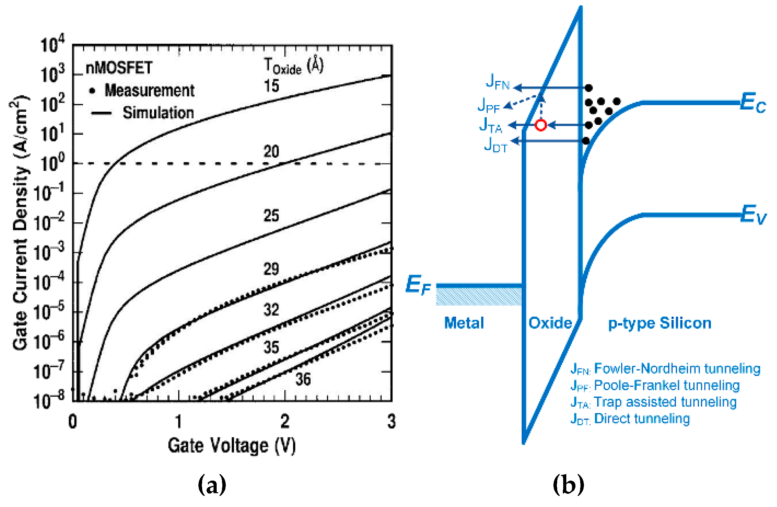
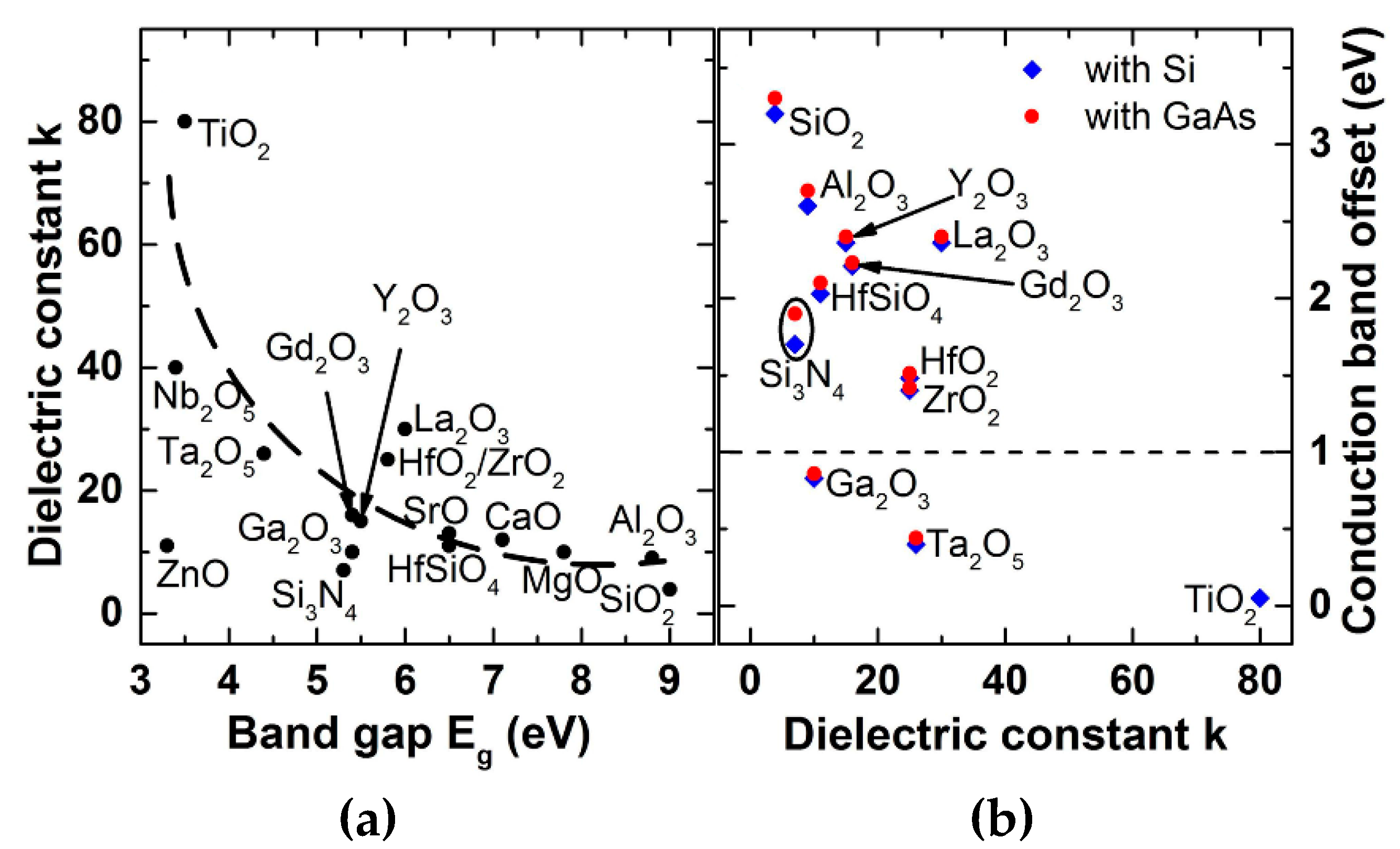
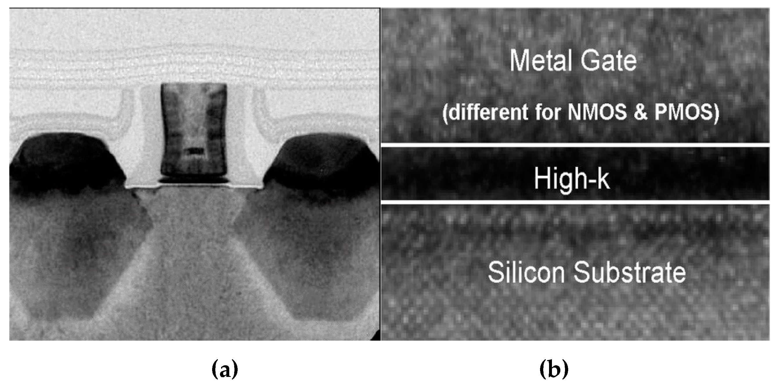
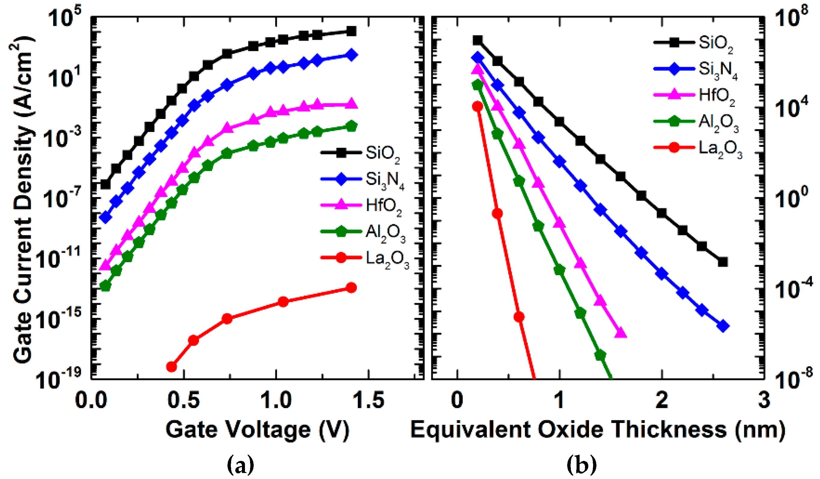
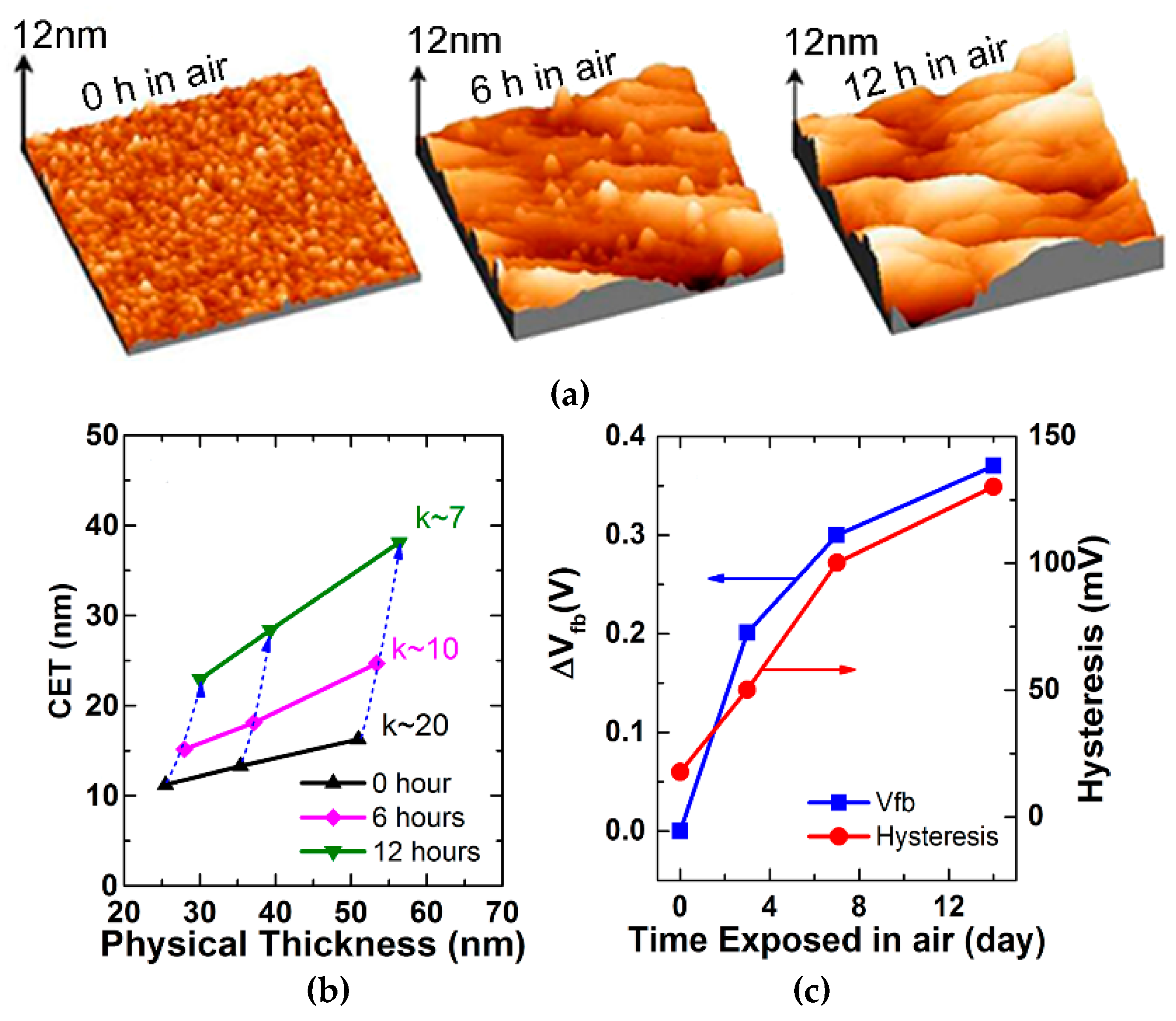
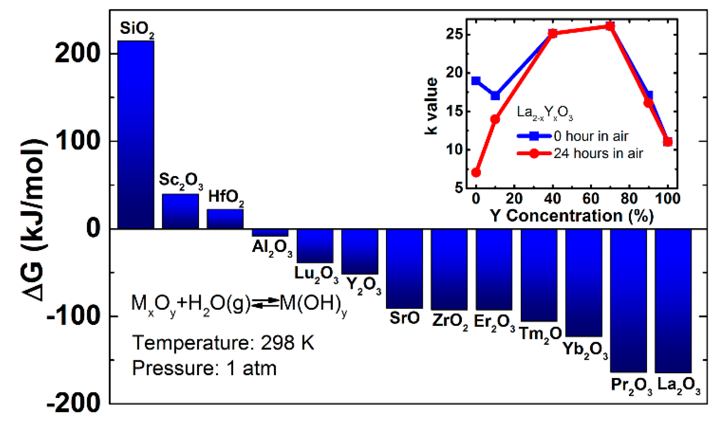
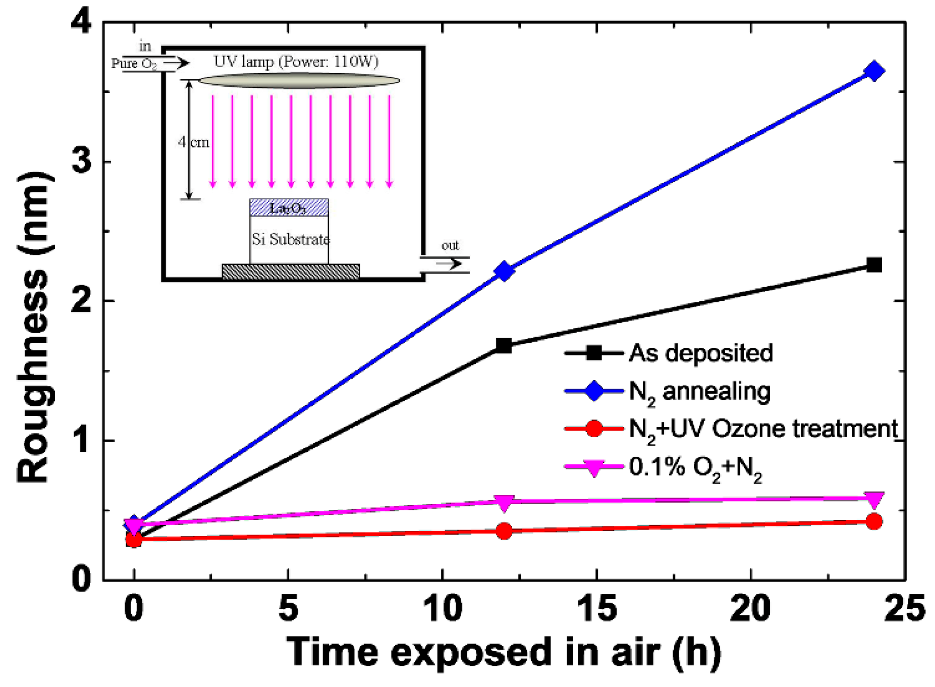
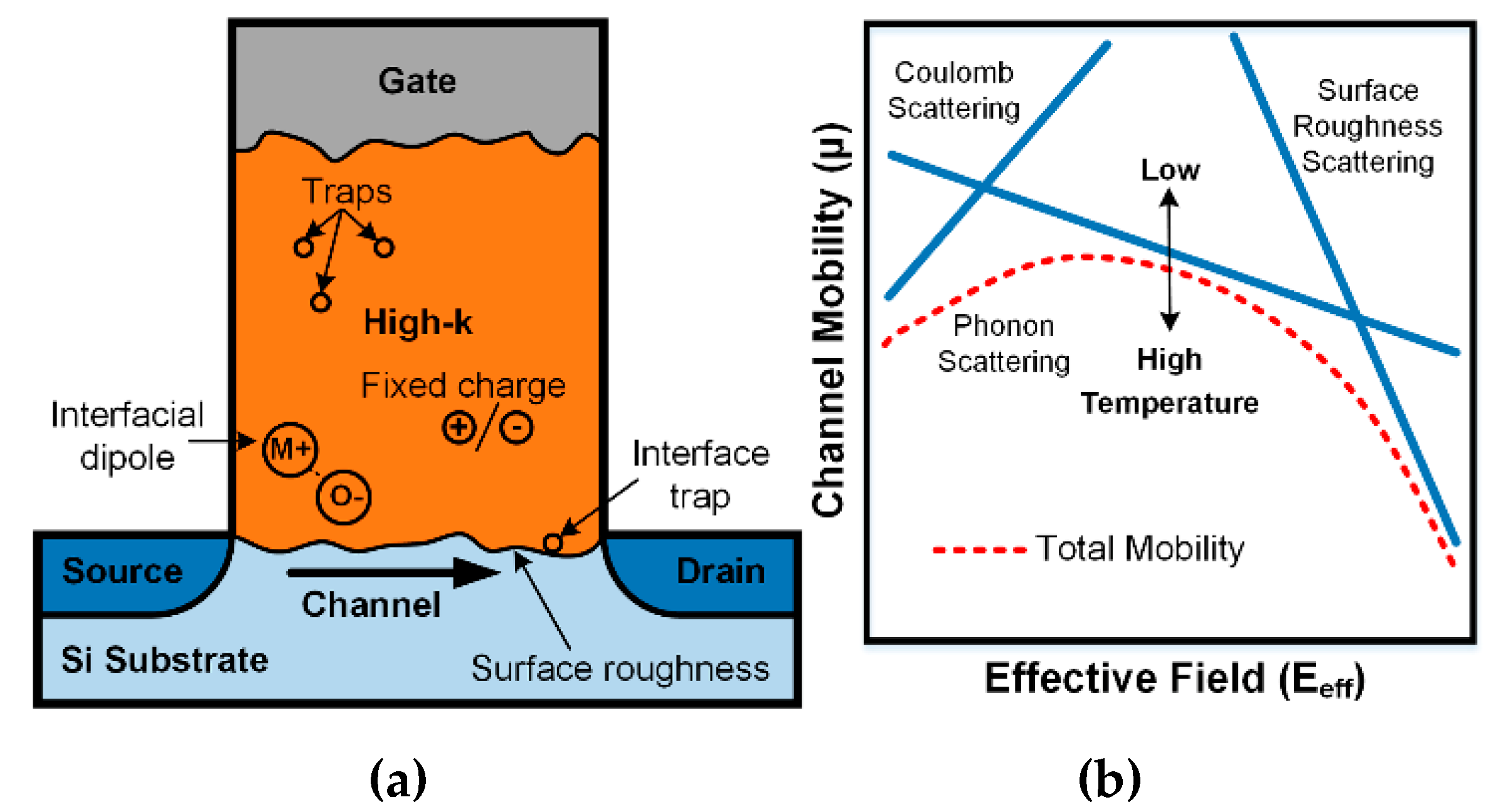
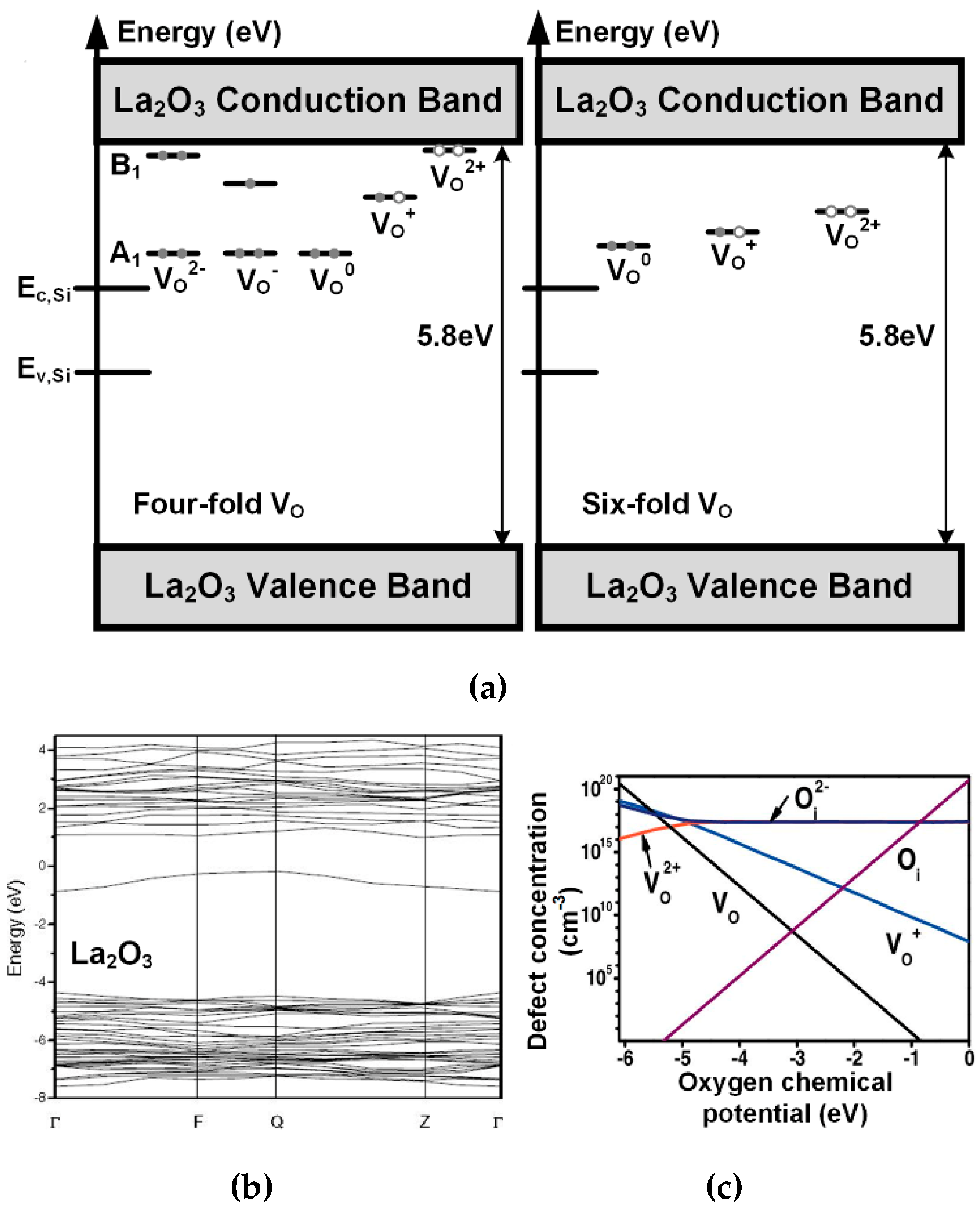
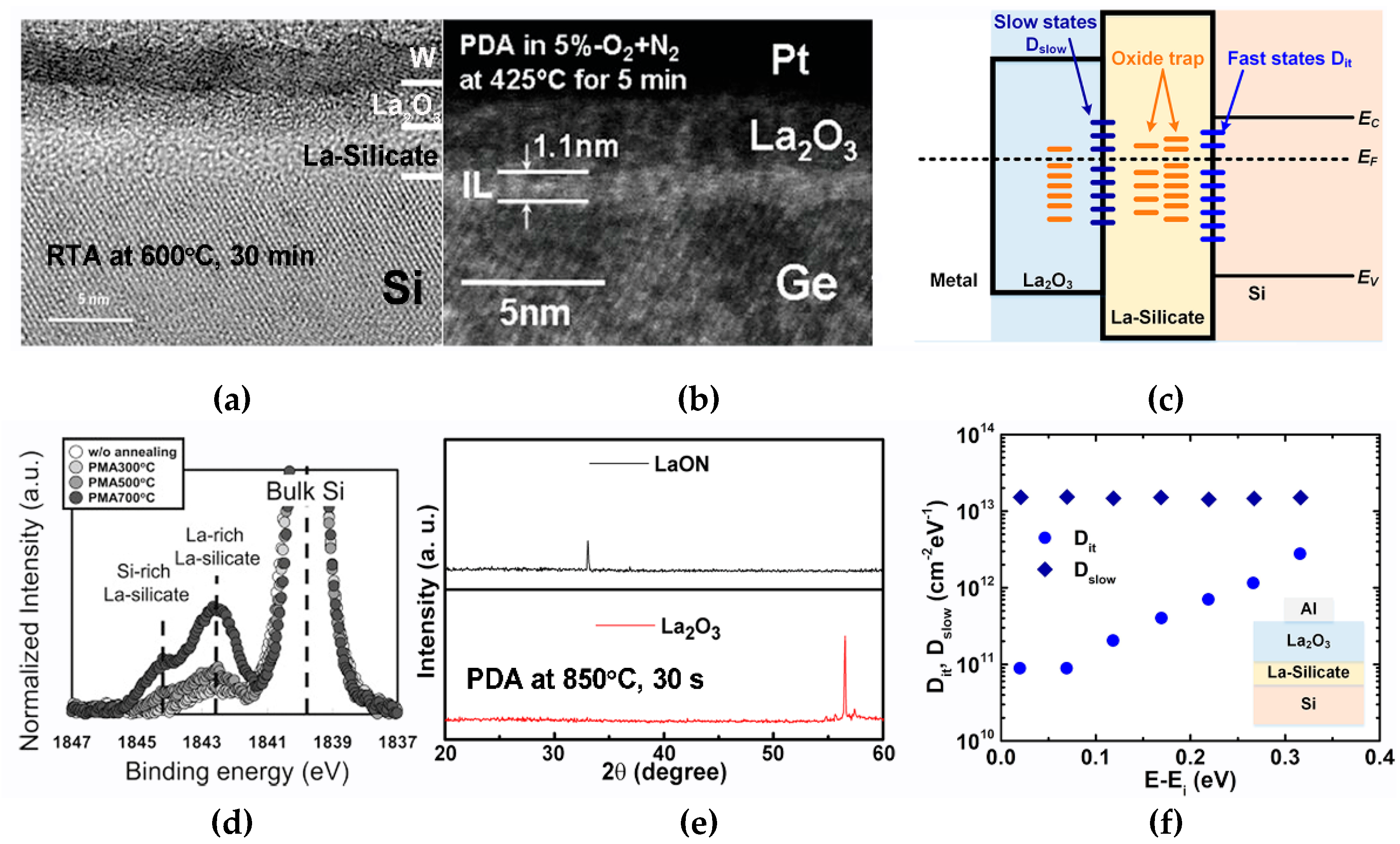
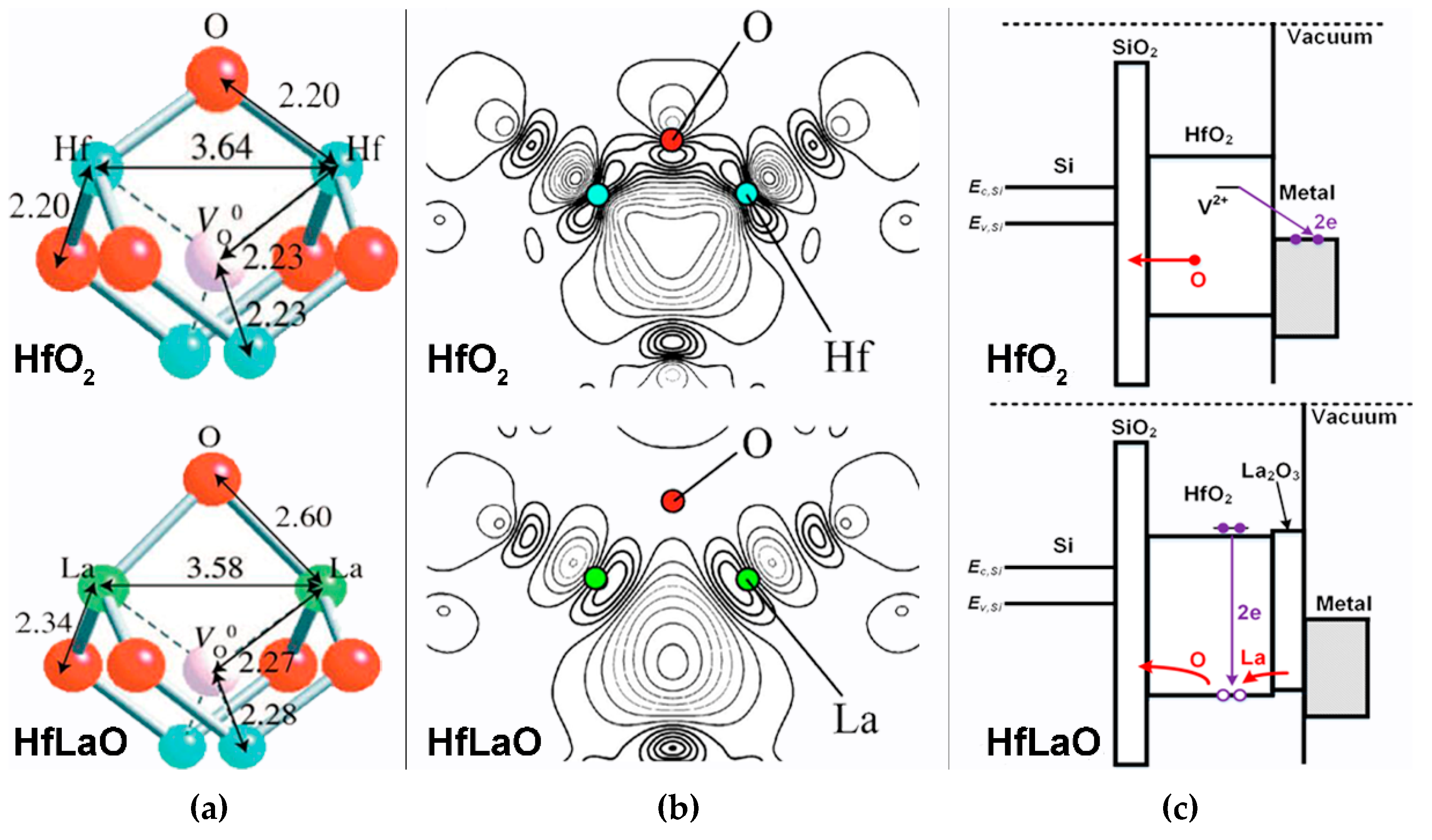
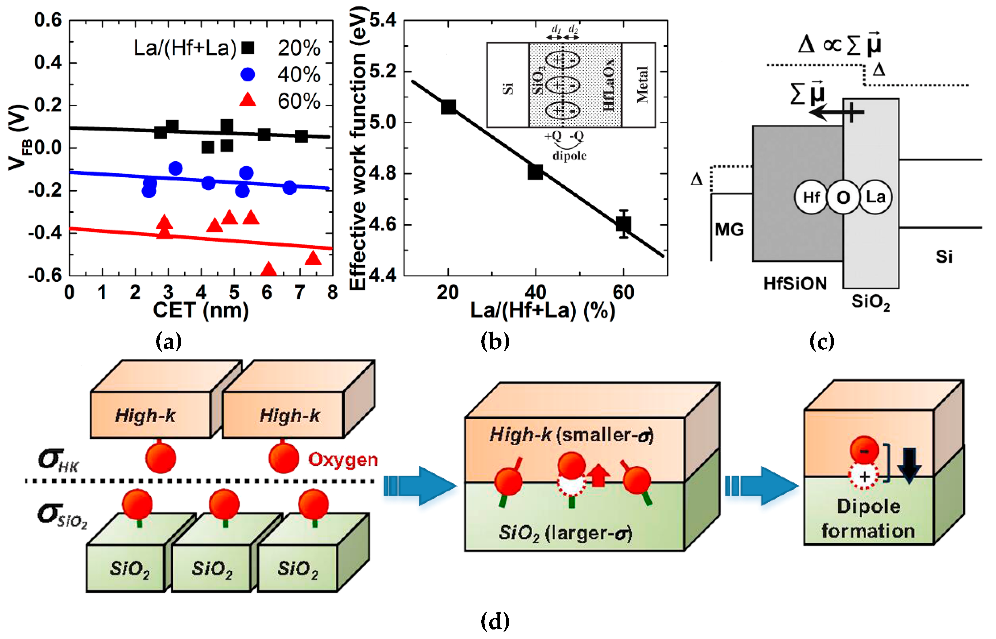
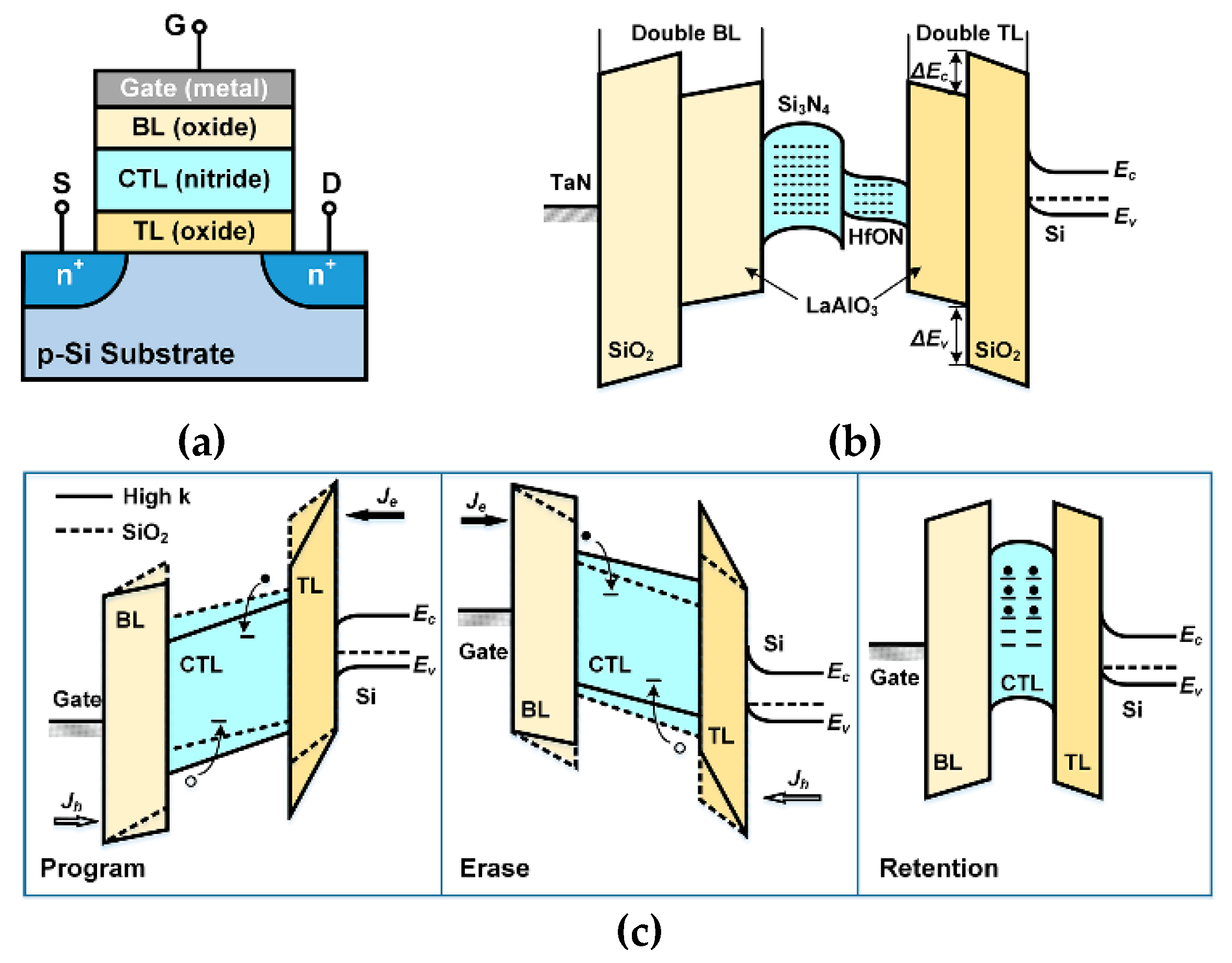
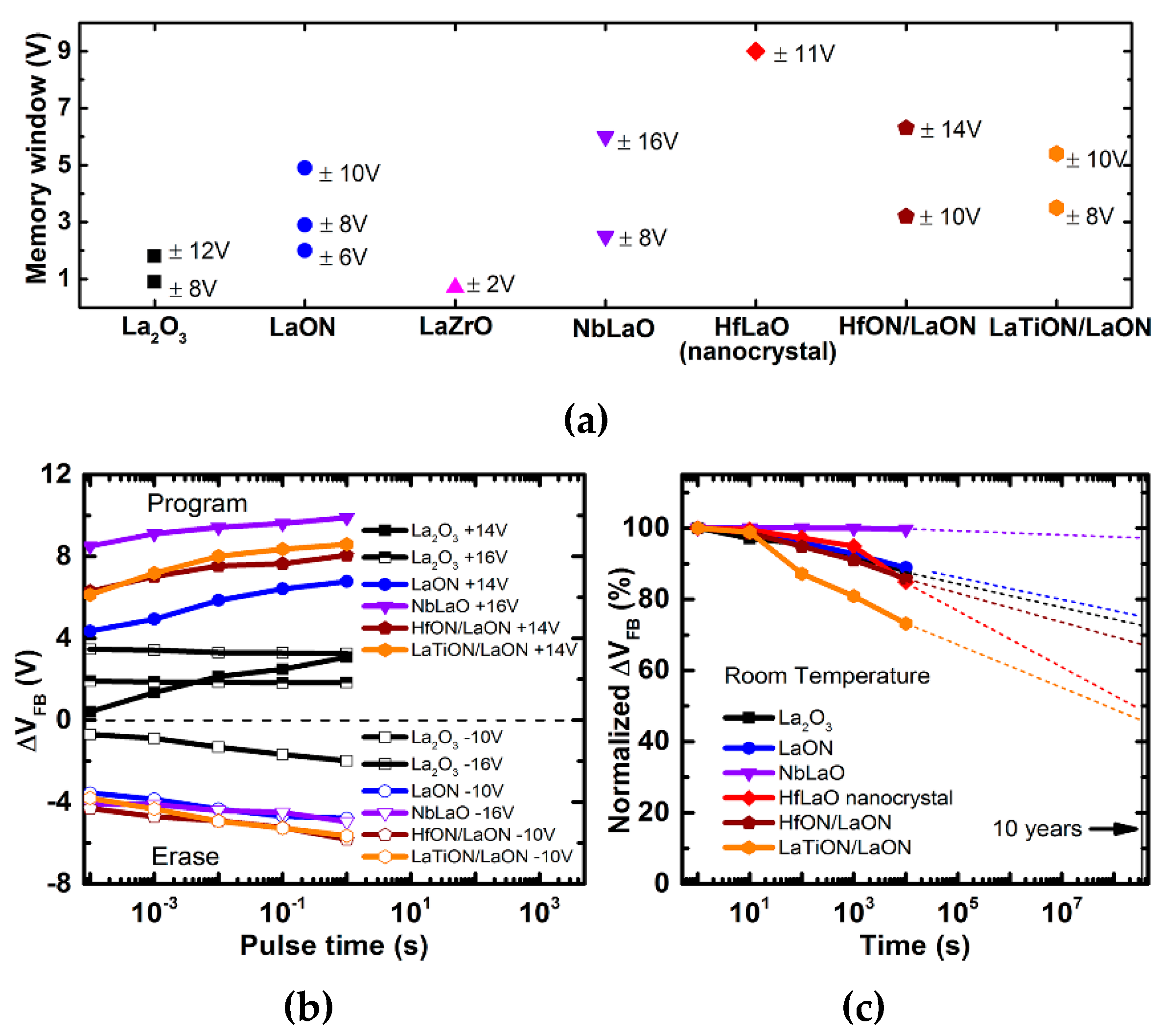
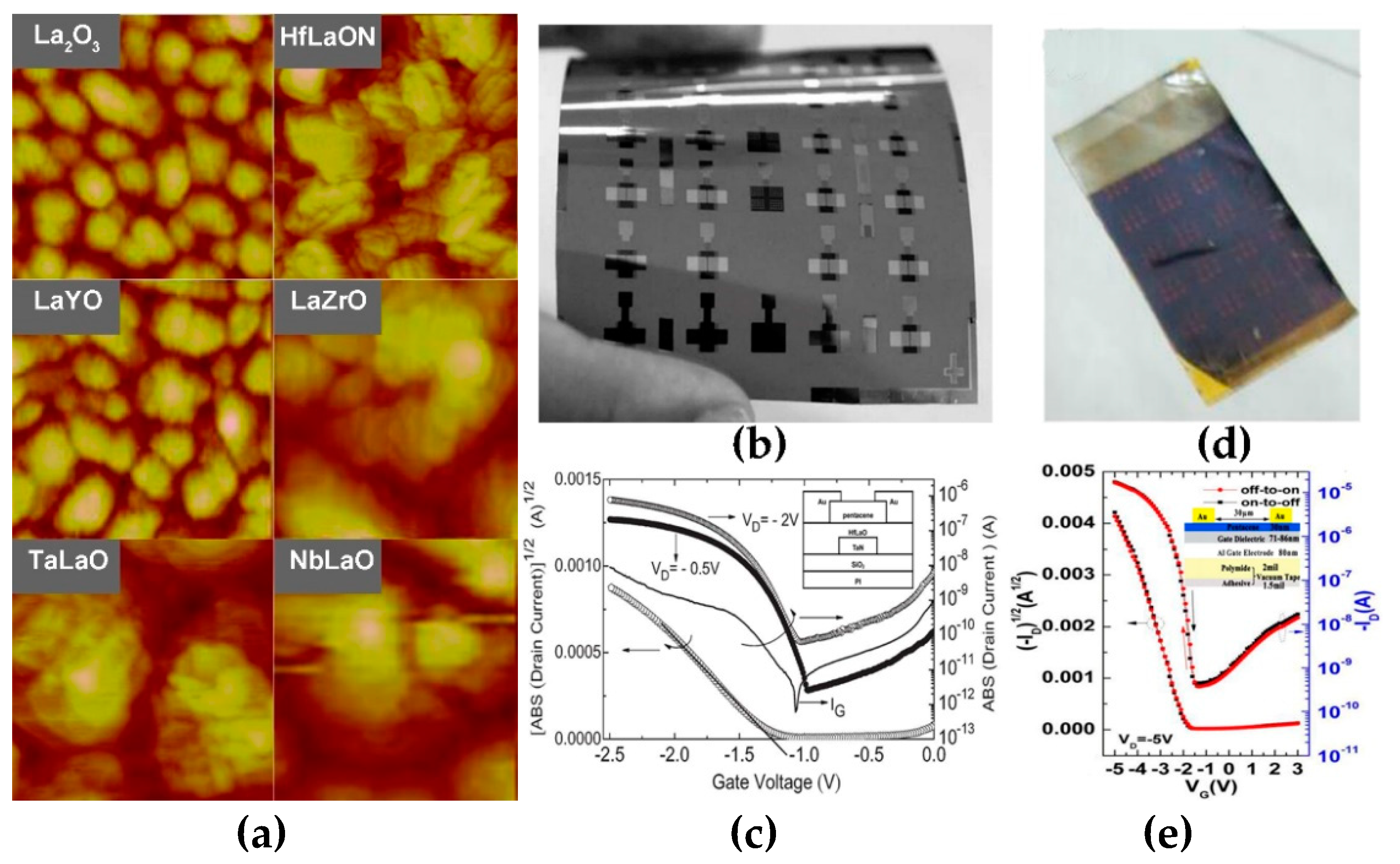
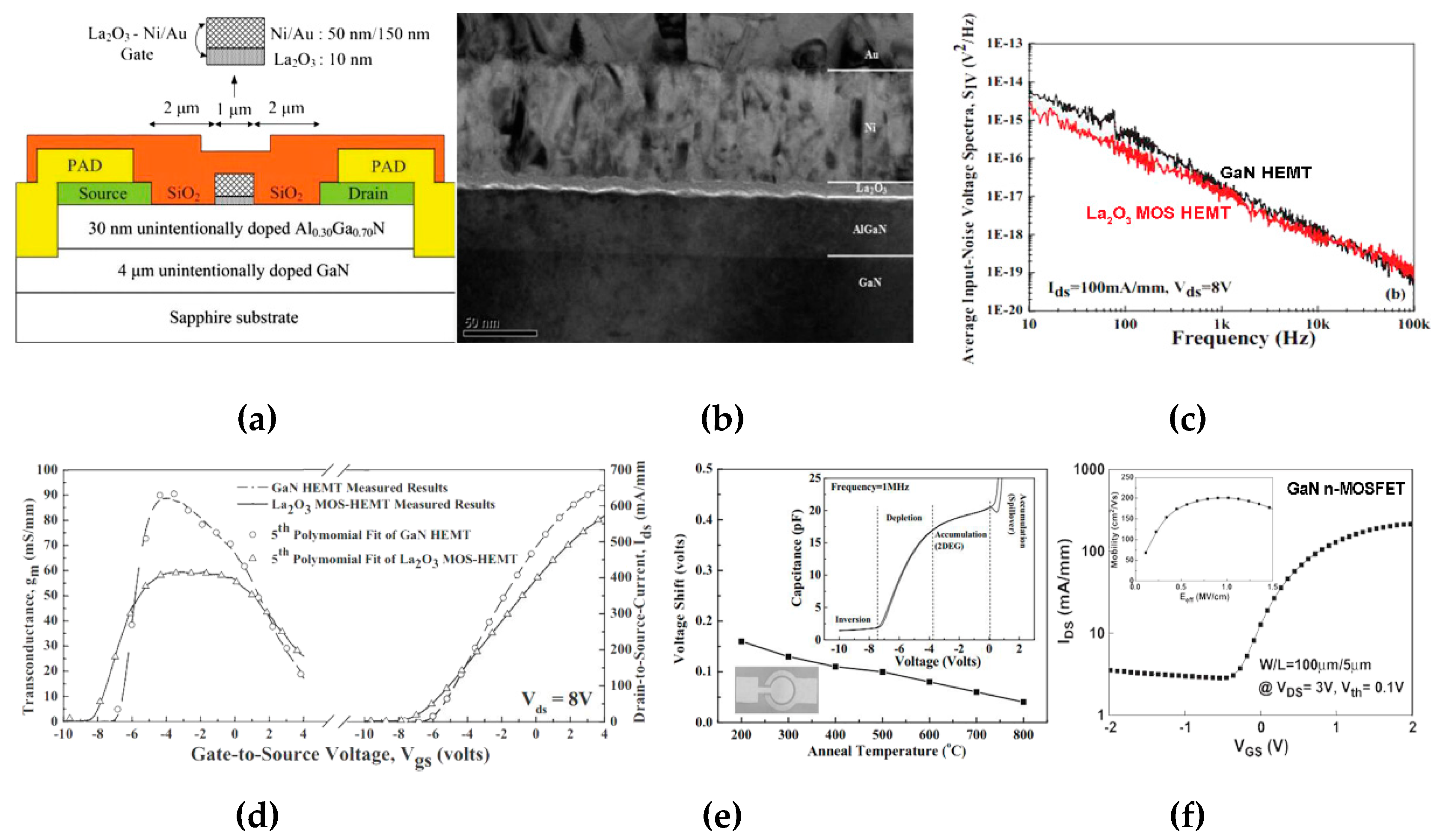
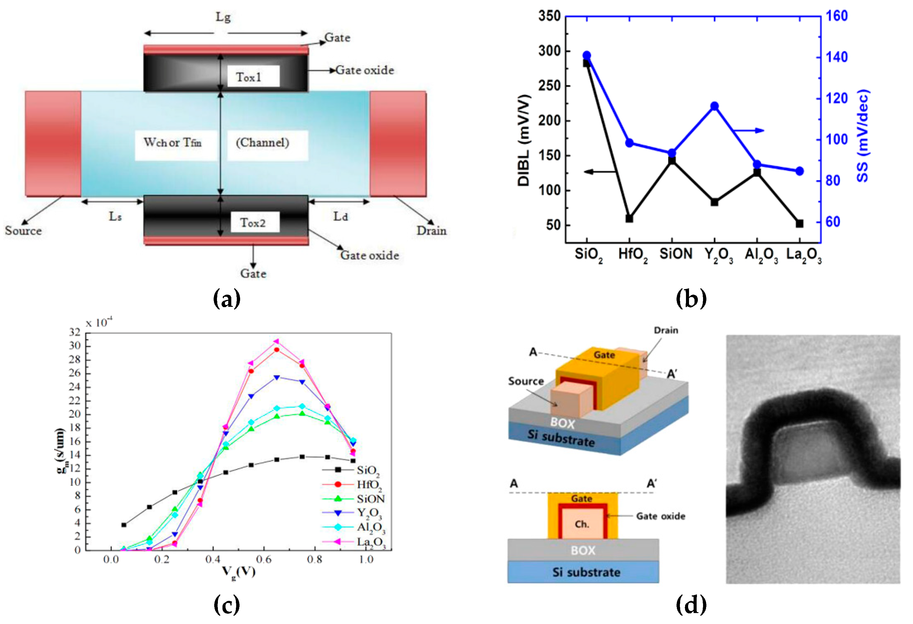
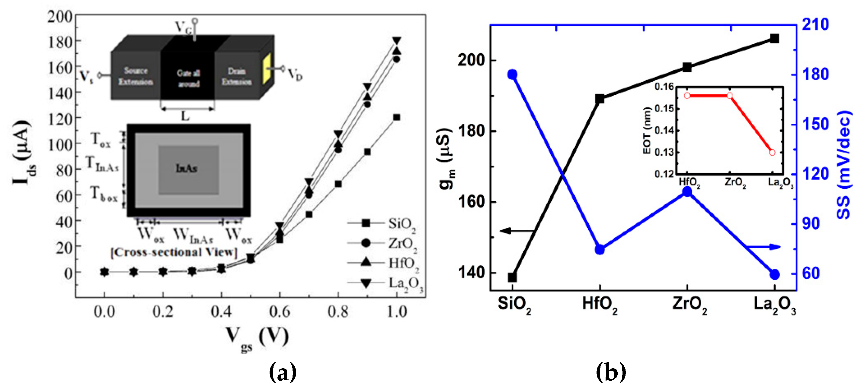
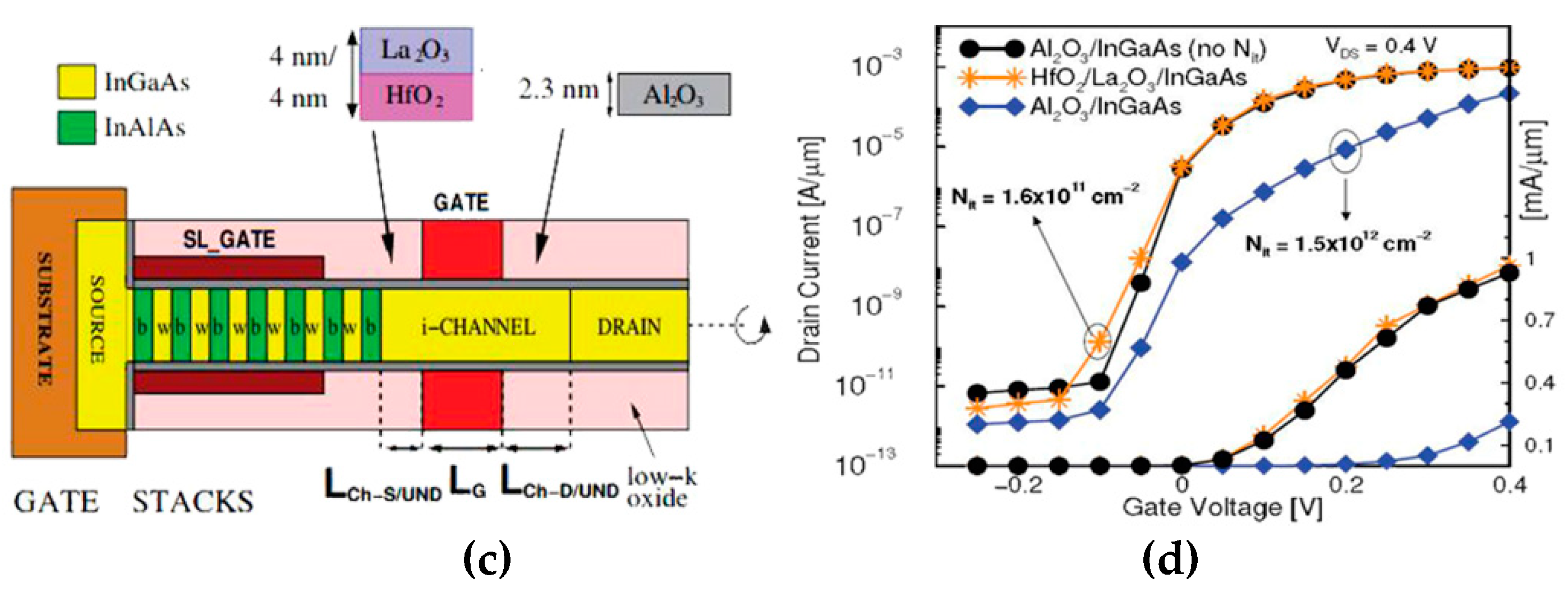
Table 1.
Key geometric parameters for several technology nodes [1].
Table 1.
Key geometric parameters for several technology nodes [1].
| Gate Length (nm) | 22 | 16 | 11 | 8 |
| Dielectric thickness (nm) | 0.8 | 0.6 | 0.4 | 0.3 |
| Junction depth (nm) | 11.0 | 8.0 | 5.5 | 4.0 |
| Channel depletion thickness (nm) | 11.0 | 8.0 | 5.5 | 4.0 |
Table 2.
Characteristics of MOSFETs with La-based high-k gate dielectrics (PVD = Physical Vapor Deposition).
Table 2.
Characteristics of MOSFETs with La-based high-k gate dielectrics (PVD = Physical Vapor Deposition).
| Dielectric | Deposition | Annealing | EOT (nm) | μeff, max (cm2/Vs) | |Vth| (V) | SS (mV/dec) |
|---|---|---|---|---|---|---|
| La2O3/LaSiO [92] | E-Beam | 500 °C, 30 min | 1.15 | 300 | 0.4 | 66 |
| LaAlO3 [97] | Sputtering | 700 °C, 30 s | 1.73 | 213 | ~0.05 | 69 |
| HfLaO [99] | Sputtering | 900 °C, 30 s | 1.3 | 225 | ~0.05 | − |
| HfLaSiO [100] | PVD | 850 °C, 1 min | 1.2 | 160 | − | − |
| LaYO [101] | E-Beam | 600 °C, 5 min | 1.7 | 181 | 0.59 | 95 |
| LaZrO [102] | ALD | 500 °C, 5 min | 1.27 | − | 0.43 | 71 |
| LaTiO [103] | PVD | 600 °C | 0.63 | 300 | 0.12 | − |
Table 3.
Characteristics of IGZO TFTs with La-based high-k gate dielectrics.
| Dielectrics | La2O3 [114] | HfLaO [114] | TaLaO [115] | NbLaO [42] | ZrLaO [116] | LaAlO3 [117] |
|---|---|---|---|---|---|---|
| µsat(cm2·V−1·s−1) | 16.6 | 35.1 | 23.4 | 28.0 | 67.2 | 5.4 |
| Vth (V) | 2.14 | 3.3 | 2.4 | 1.84 | 2.59 | 0.29 |
| Hysteresis (V) | −0.61 | −0.03 | 0.1 | −0.07 | −0.56 | − |
| Ion/Ioff (107) | 1.7 | 0.51 | 2.6 | 3.6 | 0.11 | 0.011 |
| SS (mV/dec) | 210 | 206 | 177 | 170 | 240 | 98 |
| Cox (µF/cm2) | 0.21 | 0.24 | 0.262 | 0.26 | − | 0.23 |
| k | 8.5 | 10.9 | 11.8 | 10.1 | 8.9 | 10.4 |
| RMS (nm) | 0.96 | − | 0.51 | 0.24 | 0.82 | − |
Table 4.
Characteristics of pentacene OTFTs with La-based high-k gate dielectrics.
| Dielectrics | La2O3 [118] | HfLaO [119] | HfLaON [120] | ZrLaO [121] | TaLaO [41] | LaYO [118] | NbLaO [122] |
|---|---|---|---|---|---|---|---|
| µsat(cm2·V−1·s−1) | 0.091 | 0.71 | 0.71 | 0.72 | 1.21 | 0.33 | 1.14 |
| Vth (V) | −2.51 | −1.3 | −0.69 | 0.97 | 2.66 | −2.45 | −1.35 |
| Ion/Ioff (104) | 0.87 | 10 | 1.99 | 0.96 | 3.21 | 0.24 | 29 |
| SS (V/dec) | 476 | 78 | 427 | 578 | 339 | 646 | 208 |
| Cox (µF/cm2) | 0.223 | 0.95 | 0.297 | 0.236 | 0.234 | 0.222 | 0.222 |
| k | 7.54 | 21.7 | 11.5 | 10.6 | 10.9 | 8.46 | 10.8 |
| RMS (nm) | 0.96 | − | 0.138 | − | 0.357 | − | 0.326 |
Table 5.
Characteristics of Ge MOS devices with La-based high-k oxides as IPL or gate dielectric.
| Dielectric | La2O3 [56] | ZrO2 [127] | LaON [128] | HfO2 [129] | LaTiON [130] | HfTiON [131] | HfO2 [132] |
|---|---|---|---|---|---|---|---|
| IPL | − | La2O3 | − | LaON | − | LaTaON | TaON/LaON |
| Deposition | E-beam | ALD | Sputtering | Sputtering | Sputtering | Sputtering | Sputtering |
| Tox (nm) | 5.5 | 7.5 | 8 | 10 | 8 | 7 | 8 |
| k | − | 14.7 | 18.8 | 19.2 | 24.6 | 27.7 | 20.9 |
| Jg (A/cm2) at VFB+/−1 V | 1 × 10⁻⁴ | − | 2.89 × 10⁻⁴ | 5.53 × 10⁻⁴ | 2.2 × 10⁻³ | 7.8 × 10⁻⁴ | 1.77 × 10⁻⁴ |
| CET (nm) | − | 1.92 | − | 2.0 | 1.2 | 1.1 | 1.49 |
| Dit (cm−2·ev−1) | 8 × 10¹¹ | 1.2 × 10¹² | 4.96 × 10¹¹ | 4.2 × 10¹¹ | 3.1 × 10¹¹ | 7.8 × 10¹¹ | 5.32 × 10¹¹ |
Table 6.
Characteristics of GaAs MOS devices with La-based high-k oxides as IPL or gate dielectric.
| Dielectric | La2O3 [136] | LaYO [137] | LaAlO3 [138] | LaLuO3 [139] | TaYON [140] | ZrON [141] | NbAlON [142] | LaTiON [143] |
|---|---|---|---|---|---|---|---|---|
| IPL | Si | − | − | − | LaTaON | LaGeON | LaAlON | LaON |
| Deposition | Sputtering | ALD | MBD | ALD | Sputtering | Sputtering | Sputtering | Sputtering |
| Tox (nm) | 15 | 14 | 10 | 12 | 10 | 10 | 10 | 10 |
| k | 7.5 | 22 | 6.8 | 25 | 22.9 | 12.7 | 25.5 | 25.3 |
| Jg (A/cm2) at VFB+/−1 V | 1.2 × 10⁻⁵ | − | 8 × 10⁻⁸ | − | 1.3 × 10⁻⁵ | 3.8 × 10⁻⁵ | 6.2 × 10⁻⁶ | 2.3 × 10⁻⁵ |
| CET (nm) | 7.8 | 2.48 | 5.73 | 1.87 | 1.71 | 3.07 | 1.48 | 1.54 |
| Hysteresis (mV) | 260 | − | 30 | − | 35 | 30 | 45 | − |
| Dit (cm−2·ev−1) | 1.2 × 10¹² | 5 × 10¹¹ | 5 × 10¹⁰ | 7 × 10¹¹ | 9 × 10¹¹ | 1.2 × 10¹² | 7 × 10¹¹ | 1.05 × 10¹² |
© 2019 by the authors. Licensee MDPI, Basel, Switzerland. This article is an open access article distributed under the terms and conditions of the Creative Commons Attribution (CC BY) license (http://creativecommons.org/licenses/by/4.0/).
Share and Cite
MDPI and ACS Style
Liu, L.N.; Tang, W.M.; Lai, P.T. Advances in La-Based High-k Dielectrics for MOS Applications. Coatings 2019, 9, 217. https://doi.org/10.3390/coatings9040217
AMA Style
Liu LN, Tang WM, Lai PT. Advances in La-Based High-k Dielectrics for MOS Applications. Coatings. 2019; 9(4):217. https://doi.org/10.3390/coatings9040217
Chicago/Turabian StyleLiu, L. N., W. M. Tang, and P. T. Lai. 2019. "Advances in La-Based High-k Dielectrics for MOS Applications" Coatings 9, no. 4: 217. https://doi.org/10.3390/coatings9040217
Note that from the first issue of 2016, this journal uses article numbers instead of page numbers. See further details here.