Real Time Monitoring of a UV Light-Assisted Biofunctionalization Protocol Using a Nanophotonic Biosensor

 , ,
, ,  , and
, and 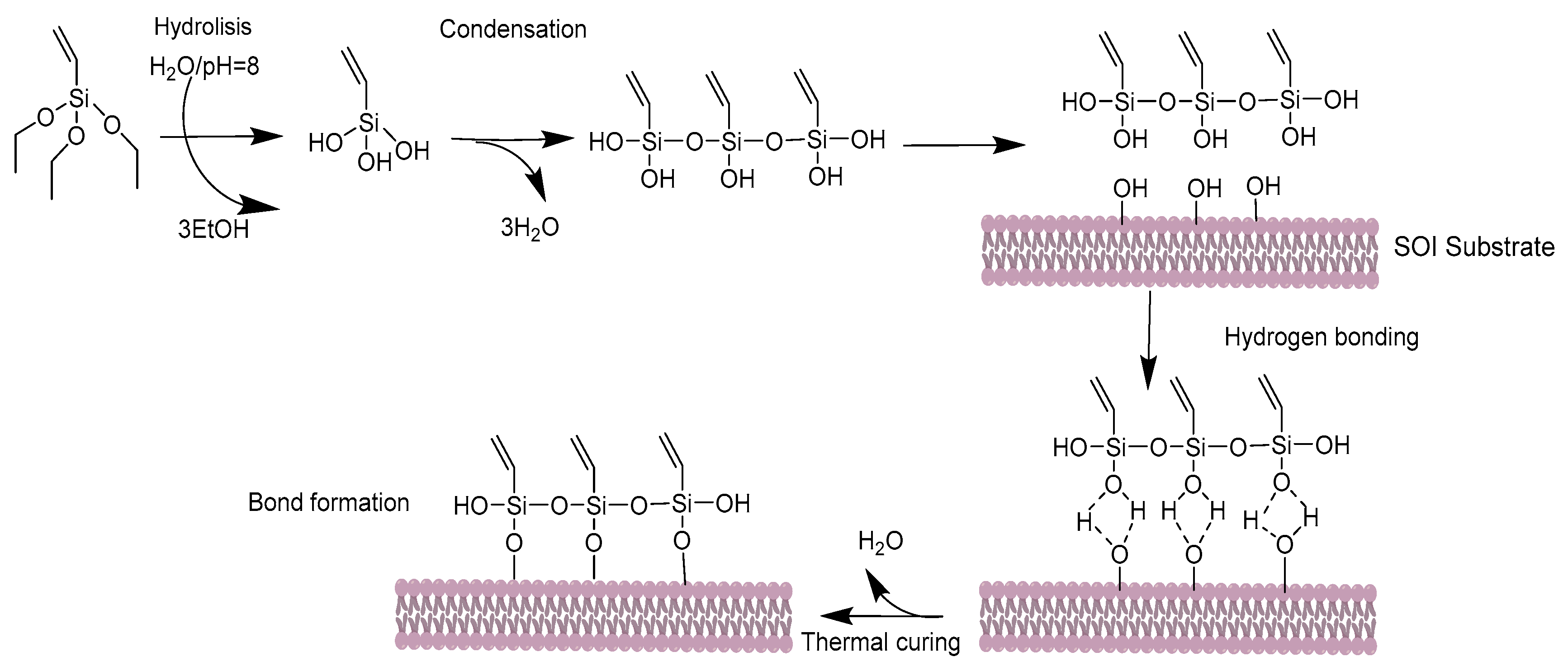
Abstract
:1. Introduction
2. Materials and Methods
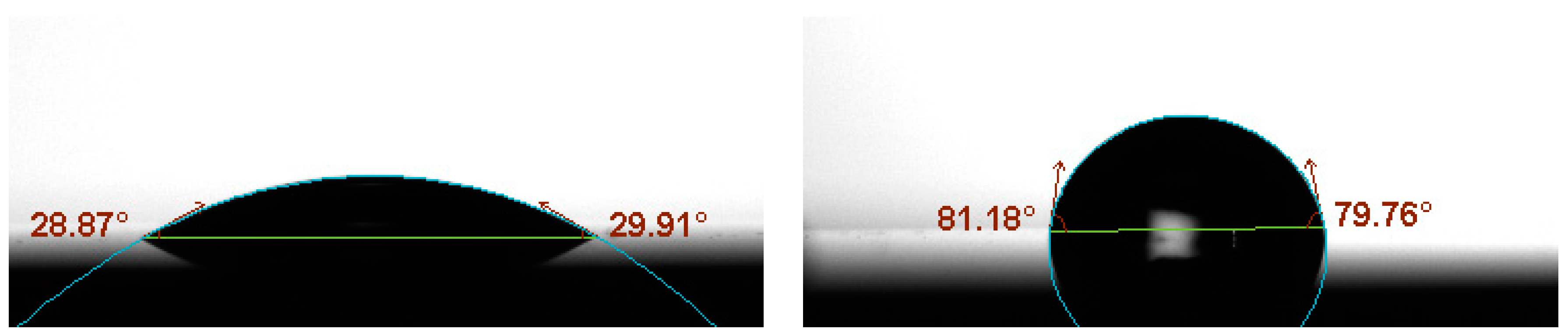
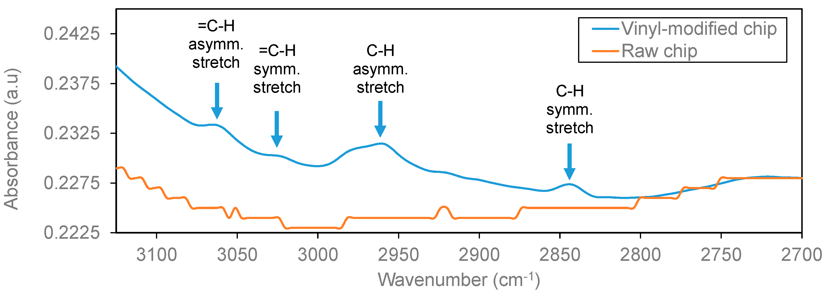
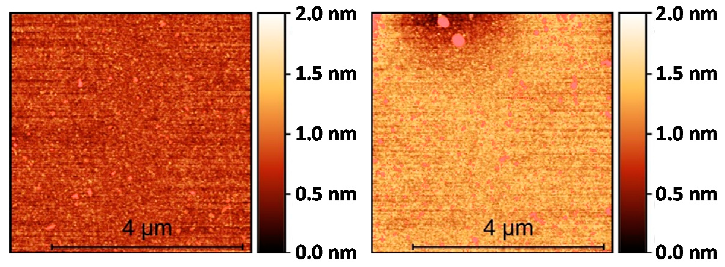
2.1. Silanization of the Silicon Surface
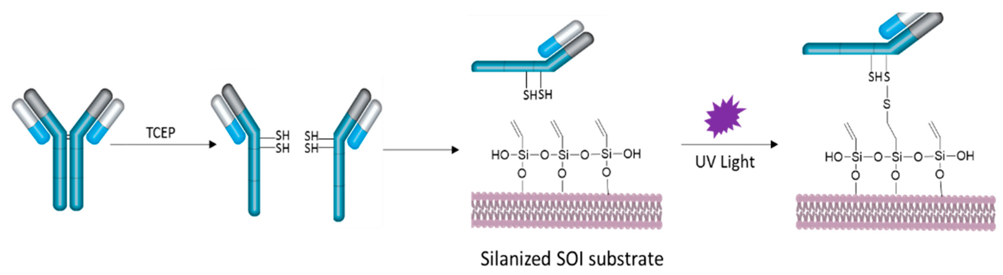
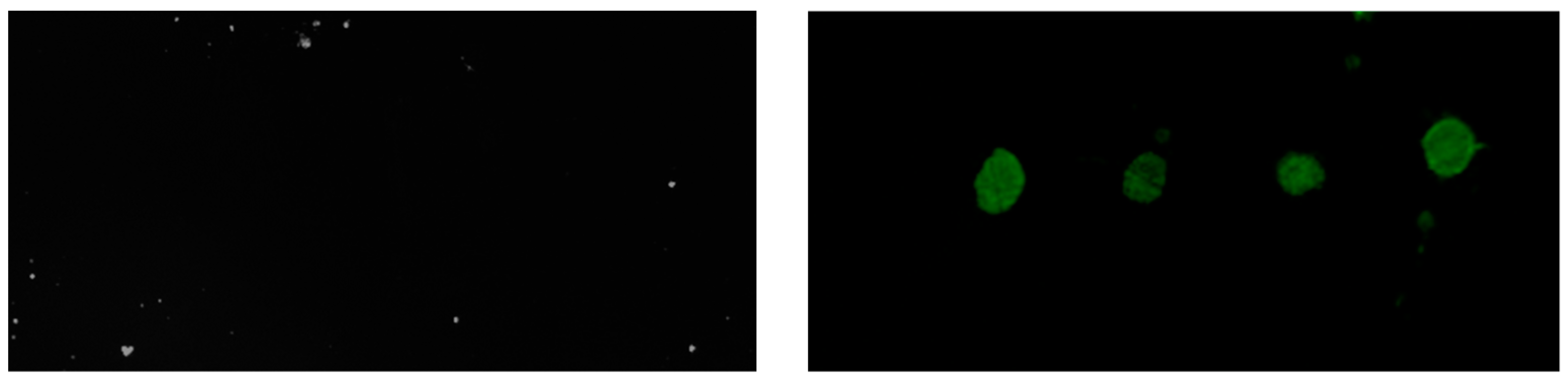
2.2. UV Light-Assisted Immobilization of Half-Antibodies
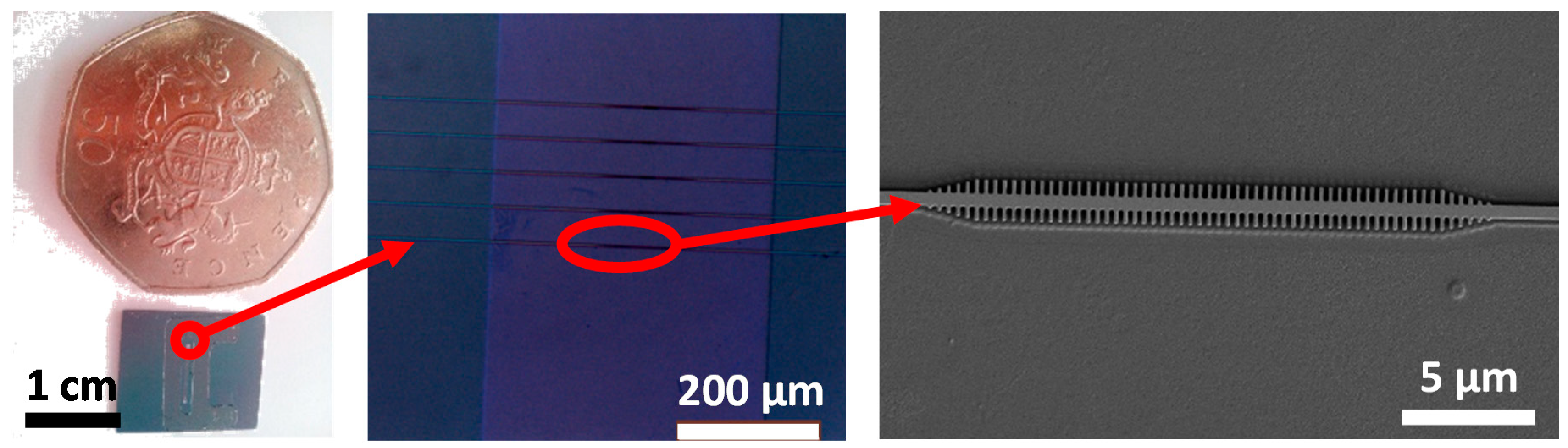
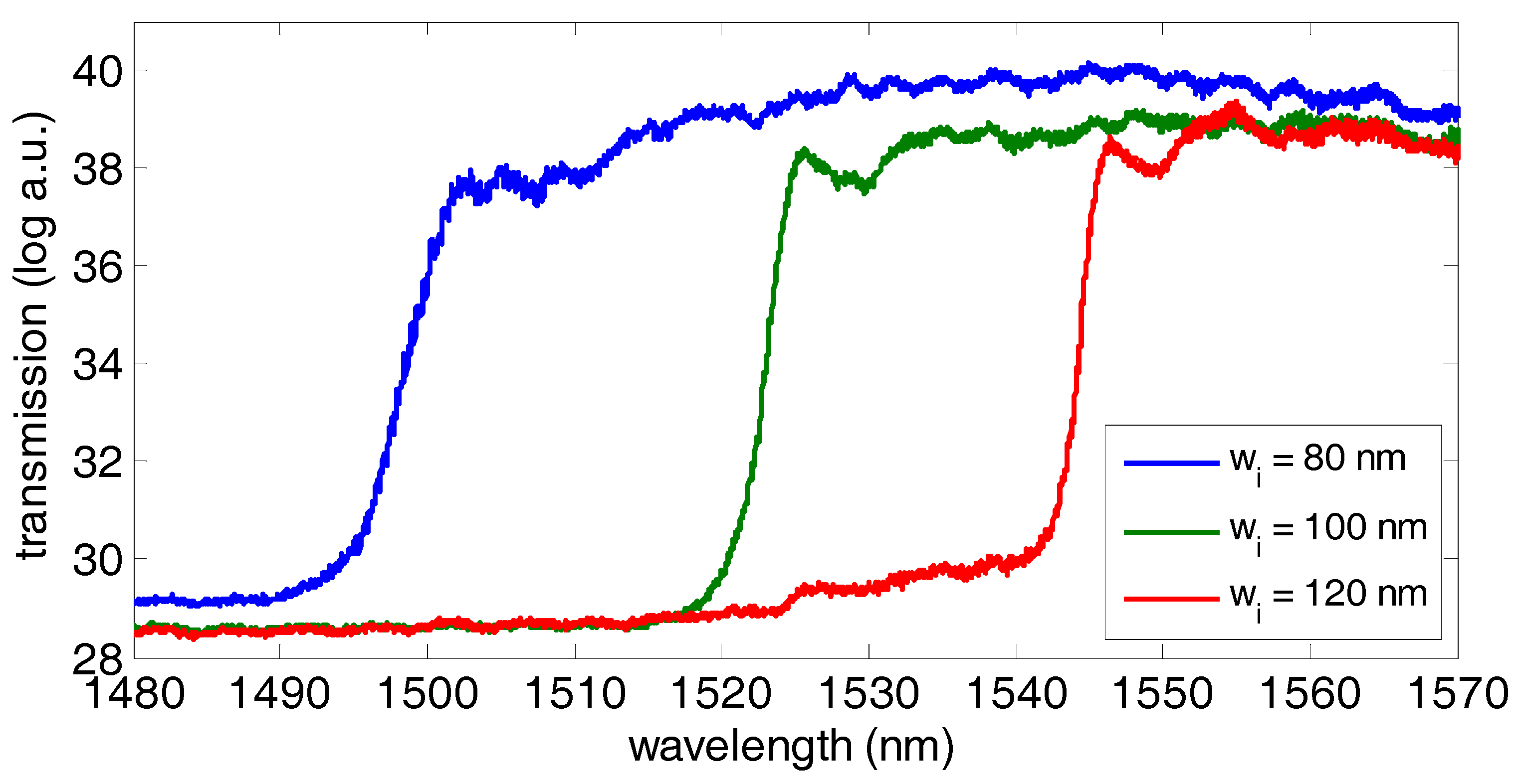
2.3. SOI Photonic Sensing Chip
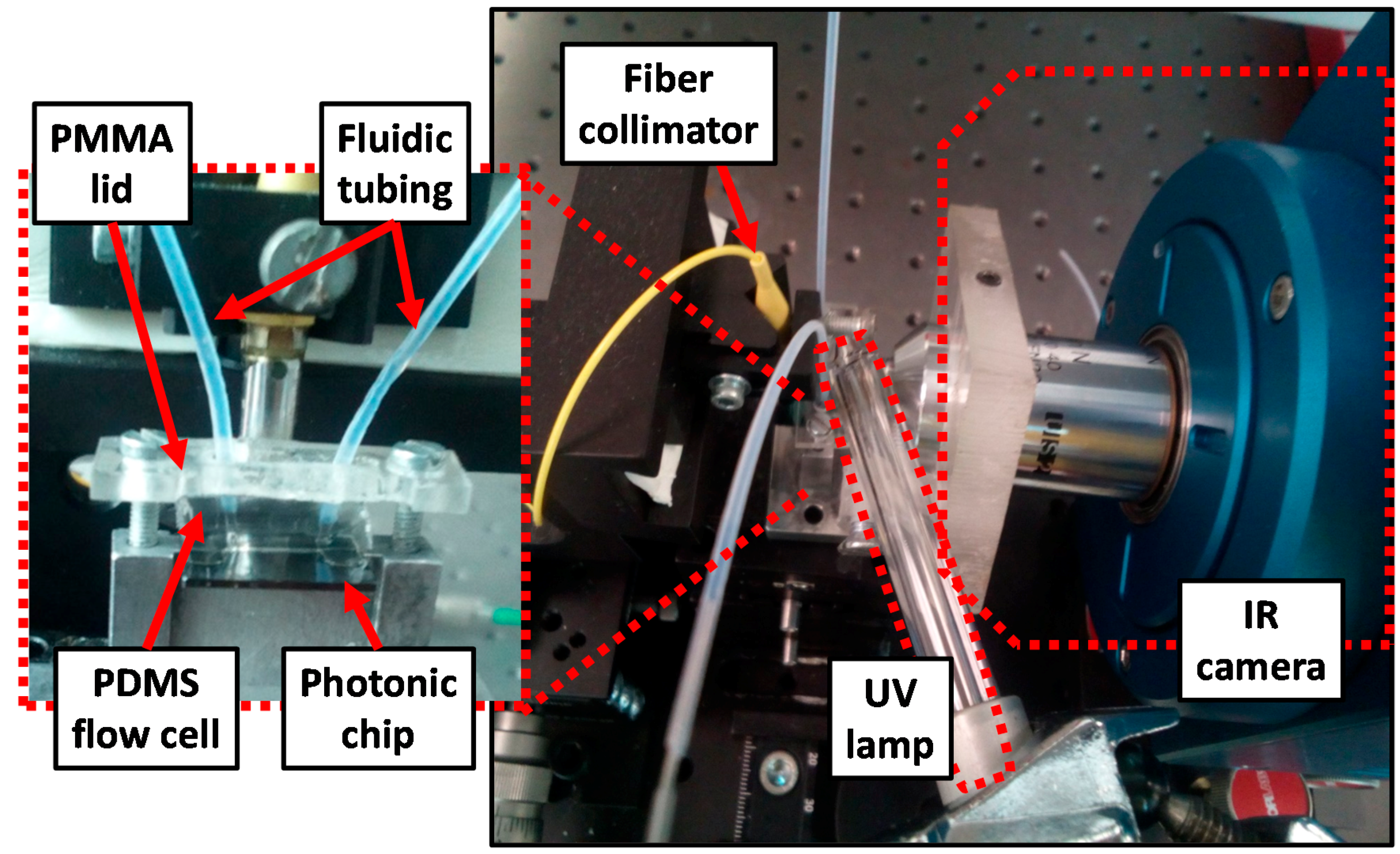
2.4. Experimental Platform
3. Results and Discussion
4. Conclusions
Author Contributions
Funding
Acknowledgments
Conflicts of Interest
References
- Chin, C.D.; Linder, V.; Sia, S.K. Lab-on-a-chip devices for global health: Past studies and future opportunities. Lab Chip 2007, 7, 41–57. [Google Scholar] [CrossRef] [PubMed]
- Wu, J.; Dong, M.; Santos, S.; Rigatto, C.; Liu, Y.; Lin, F. Lab-on-a-Chip Platforms for Detection of Cardiovascular Disease and Cancer Biomarkers. Sensors 2017, 17, 2934. [Google Scholar] [CrossRef] [PubMed]
- Estevez, M.; Alvarez, M.; Lechuga, L. Integrated optical devices for lab-on-a-chip biosensing applications. Laser Photonics Rev. 2012, 6, 463–487. [Google Scholar] [CrossRef]
- Vestergaard, M.; Kerman, K.; Tamiya, E. An overview of label-free electrochemical protein sensors. Sensors 2007, 7, 3442–3458. [Google Scholar] [CrossRef] [PubMed]
- Johnson, B.N.; Mutharasan, R. Biosensing using dynamic-mode cantilever sensors: A review. Biosens. Bioelectron. 2012, 32, 1–18. [Google Scholar] [CrossRef] [PubMed]
- Jonkheijm, P.; Weinrich, D.; Schröder, H.; Niemeyer, C.M.; Waldmann, H. Chemical Strategies for Generating Protein Biochips. Angew. Chem. Int. Ed. 2008, 47, 9618–9647. [Google Scholar] [CrossRef] [PubMed]
- Phaner-Goutorbe, M.; Dugas, V.; Chevolot, Y.; Souteyrand, E. Silanization of silica and glass slides for DNA microarrays by impregnation and gas phase protocols: A comparative study. Mater. Sci. Eng. C 2011, 31, 384–390. [Google Scholar] [CrossRef]
- Escorihuela, J.; Bañuls, M.J.; Grijalvo, S.; Eritja, R.; Puchades, R.; Maquieira, A. Direct covalent attachment of DNA microarrays by rapid thiol-Ene “click” chemistry. Bioconj. Chem. 2014, 25, 618–627. [Google Scholar] [CrossRef] [PubMed]
- Escorihuela, J.; Bañuls, M.J.; Puchades, R.; Maquieira, A. DNA microarrays on silicon surfaces through thiol-ene chemistry. Chem. Commun. 2012, 48, 2116–2118. [Google Scholar] [CrossRef] [PubMed]
- González-Lucas, D.; Bañuls, M.J.; García-Rupérez, J.; Maquieira, Á. Covalent attachment of biotinylated molecular beacons via thiol-ene coupling. A study on conformational changes upon hybridization and streptavidin binding. Microchim. Acta 2017, 184, 3231–3238. [Google Scholar] [CrossRef] [Green Version]
- Alonso, R.; Jiménez-Meneses, P.; García-Rupérez, J.; Bañuls, M.J.; Maquieira, Á. Thiol-ene click chemistry towards easy microarraying of half-antibodies. Chem. Commun. 2018, 54, 6144–6147. [Google Scholar] [CrossRef] [PubMed]
- González-Guerrero, A.B.; Álvarez, M.; Castaño, A.G.; Domínguez, C.; Lechuga, L.M. A comparative study of in-flow and micro-patterning biofunctionalization protocols for nanophotonic silicon-based biosensors. J. Colloid Interface Sci. 2013, 393, 402–410. [Google Scholar] [CrossRef] [PubMed] [Green Version]
- Povinelli, M.; Johnson, S.; Joannopoulos, J. Slow-light, band-edge waveguides for tunable time delays. Opt. Express 2005, 13, 7145–7159. [Google Scholar] [CrossRef] [PubMed]
- Ruiz-Tórtola, Á.; Prats-Quílez, F.; González-Lucas, D.; Bañuls, M.J.; Maquieira, Á.; Wheeler, G.; Dalmay, T.; Griol, A.; Hurtado, J.; García-Rupérez, J. High sensitivity and label-free oligonucleotides detection using photonic bandgap sensing structures biofunctionalized with molecular beacon probes. Biomed. Opt. Express 2018, 9, 1717–1727. [Google Scholar] [CrossRef] [PubMed] [Green Version]
- Sandeep, A.; Saleem, K.; Akhil, V.; Harneet, K.; Parveen, L. Microfluidics mechanics and applications: A review. J. Nano Electron. Phys. 2013, 5, 04047. [Google Scholar]
- Golas, A.; Pardhi, P.; Dimachkie, Z.O.; Siedlecki, C.A.; Vogler, E.A. Surface-energy dependent contact activation of blood factor XII. Biomaterials 2010, 31, 1068–1079. [Google Scholar] [CrossRef] [PubMed] [Green Version]


© 2018 by the authors. Licensee MDPI, Basel, Switzerland. This article is an open access article distributed under the terms and conditions of the Creative Commons Attribution (CC BY) license (http://creativecommons.org/licenses/by/4.0/).
Share and Cite
Sabek, J.; Torrijos-Morán, L.; Griol, A.; Díaz Betancor, Z.; Bañuls Polo, M.-J.; Maquieira, Á.; García-Rupérez, J. Real Time Monitoring of a UV Light-Assisted Biofunctionalization Protocol Using a Nanophotonic Biosensor. Biosensors 2019, 9, 6. https://doi.org/10.3390/bios9010006
Sabek J, Torrijos-Morán L, Griol A, Díaz Betancor Z, Bañuls Polo M-J, Maquieira Á, García-Rupérez J. Real Time Monitoring of a UV Light-Assisted Biofunctionalization Protocol Using a Nanophotonic Biosensor. Biosensors. 2019; 9(1):6. https://doi.org/10.3390/bios9010006
Chicago/Turabian StyleSabek, Jad, Luis Torrijos-Morán, Amadeu Griol, Zeneida Díaz Betancor, María-José Bañuls Polo, Ángel Maquieira, and Jaime García-Rupérez. 2019. "Real Time Monitoring of a UV Light-Assisted Biofunctionalization Protocol Using a Nanophotonic Biosensor" Biosensors 9, no. 1: 6. https://doi.org/10.3390/bios9010006