
Application of Single-Electron Transistor to Biomolecule and Ion Sensors

Research Institute for Nanodevice and Bio Systems, Hiroshima University, 1-4-2 Kagamiyama, Higashihiroshima, Hiroshima 739-8527, Japan
Appl. Sci. 2016, 6(4), 94; https://doi.org/10.3390/app6040094
Submission received: 30 December 2015
/
Revised: 1 March 2016
/
Accepted: 18 March 2016
/
Published: 31 March 2016
(This article belongs to the Special Issue Applied Single-Electron Transistors)
Abstract
:The detection and quantification of chemical and biological species are the key technology in many areas of healthcare and life sciences. Field-effect transistors (FETs) are sophisticated devices used for the label-free and real-time detection of charged species. Nanowire channels were used for highly sensitive detections of target ion or biomolecule in FET sensors, however, even significantly higher detection sensitivity is required in FET sensors, especially when the target species are dilute in concentration. Since the high detection sensitivity of nanowire FET sensors is due to the suppression of the carrier percolation effect through the channel, the channel width has to be decreased, leading to the decrease in the transconductance (gm). Therefore, gm should be increased while keeping channel width narrow to obtain higher sensitivity. Single-electron transistors (SETs) are a promising candidate for achieving higher detection sensitivity due to the Coulomb oscillations. However, no reports of an SET-based ion sensor or biosensor existed, probably because of the difficulty of the room-temperature operation of SETs. Recently, room-temperature SET operations were carried out using a Si multiple-island channel structure. This review introduces the mechanism of ultra-sensitive detection of ions and biomolecules based on an SET sensor and the experimental results.
1. Introduction
The detection and quantification of chemical and biological species are crucial to many areas of healthcare and life sciences, ranging from the diagnosis of disease to the discovery of new drug molecules. The need exists also in the security and environmental fields. Various types of devices are now in production and being developed to meet this need. For the devices, radioactive or fluorescent markers are used in many cases. Since the methods using such markers involve time-consuming and multi-stage processes that are expensive and unsuitable for real-time detections, devices without such markers are desired for detection and quantification.
Field effect transistors (FETs) are sophisticated devices used for label-free and real-time detections of ions and charged molecules. Ion-sensitive FETs (ISFETs) were first reported by Bergveld [1]. Electrical characteristics of ISFETs change in response to the concentration and type of ion present in the aqueous solution on the gate insulator surface. Following the report, ion sensors and biosensors based on Si metal-oxide-semiconductor FETs (MOSFETs) were developed for the detection of various chemical species and biomolecules. Detections based on an FET measure the charge change accompanied by the specific molecular recognition events on the gate or the gate insulator surface. Gotoh et al. fabricated biosensors based on a Si MOSFET for the detection of adenosine-5′-triphosphate (ATP) [2]. Park et al. detected ribosomal protein using a Si MOSFET [3]. Kim et al. [4] and Sakata et al. [5] detected target deoxyribonucleic acid (DNA) using Si MOSFETs with the probe DNA immobilized on the gate surface and the channel surface, respectively.
FETs used for ion sensors and/or biosensors are not limited to Si MOSFETs. Graphene FETs were also used for detecting DNA [6], bacteria [6], protein and ions [7]. Organic FETs were also used for label-free DNA detection [8]. Compared with these non-Si FET sensors, sensors with a Si MOSFET have the merit of being able to be highly integrated on a single chip for the simultaneous detection and quantification of various ions and biomolecules by utilizing mature large scale integration (LSI) techniques.
Nanowire FETs for the sensors are substantially more sensitive than the conventional FETs having a wide channel; this is because carriers in a narrow channel are more effectively affected by the charge on the gate insulator than those in a wide channel. Highly sensitive detections of target ions or biomolecules were reported using nanowire channels in FET sensors [9,10,11,12,13,14,15,16,17,18,19]. There are two types of nanowire fabrication methods. One is the bottom up method utilizing the self-assembled mechanism of atoms and molecules. The other is the top down method using electron beam (EB) lithography. For Si nanowires fabricated using the bottom up method, the following reports exist. Cui et al. detected streptavidin using biotin-modified Si nanowire FETs [9]. Here, streptavidin and biotin are kinds of protein, and the ligand-receptor binding of biotin-streptavidin is well known. The Si nanowire was fabricated using the chemical vapor deposition with gold nanoclusters as catalysts. Using Si nanowire FETs fabricated with this method, electrical detections were also achieved for a single virus of influenza A [10], interactions between ATP and a protein [11], and prostate-specific antigen (PSA) [12]. Here, PSA is a widely used protein biomarker for prostate cancer. For Si nanowires fabricated using the top down methods, on the other hand, the following reports exist. Stern et al. demonstrated immunodetections of mouse-immunoglobulin G and mouse-immunoglobulin A [13]. Li et al. detected target DNA in solution with the probe DNA (12-mer oligonucleotide) attached on the nanowire surface [14]. Kim et al. detected PSA with the antibody of PSA (anti-PSA) immobilized on the nanowire surface [15]. Kudo et al. [16] and Knopfmacher et al. [17] fabricated pH sensors. Materials other than Si were also used for nanowire FET biosensors. Carbon nanotubes are the typical material and were used for label-free protein biosensors [18,19].
However, FET sensors with even higher sensitivity than that of nanowire FET sensors for the detection of target species are preferable and desired, especially in a dilute solution of target ions or molecules. Single-electron transistors (SETs) are a promising candidate for achieving even higher detection sensitivity due to the Coulomb oscillations. There had been no reports on SET-based ion sensors or biosensors, probably due to the difficulty of the room-temperature operation of SETs and incompatibility of biomolecule solution processes with LSI fabrication processes. Recently, using a Si multiple-island channel structure for the room-temperature operation of SETs and the appropriate gate insulator structure for the solution processes, a pH sensor [20] and biomolecule sensors for the detection of streptavidin [21,22] were developed based on SETs. The immunodetection of PSA has been also demonstrated using an SET [22].
In this review, following this introduction, the mechanism for the ultrahigh-sensitive detection of ions and biomolecules using an SET sensor is first explained, and compared with the detection mechanism using a nanowire FET sensor. Second, there is a description of how to fabricate room-temperature operating SETs and the sensors with them. Then, the experimental results of pH, streptavidin, and PSA detections with SET sensors are introduced with their surface modification methods of the gate insulator. Finally, summaries with future prospective are provided.
2. Mechanism of High Sensitivity in Biomolecule Detection Based on a Single-Electron Transistor
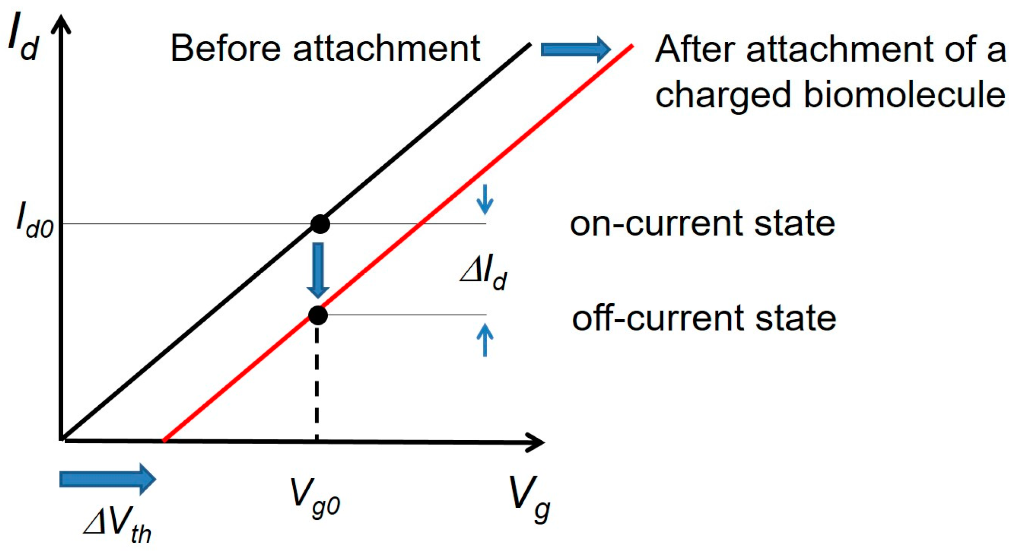
After the attachment of charged biomolecule, drain current (Id) changes from an on-current state (Id0) to an off-current state at the same gate voltage (Vg0) due to the threshold voltage shift (ΔVth) of Id-Vg curve (Figure 1). Therefore, sensitivity is closely related to both magnitudes of ΔVth and the change amount of Id (ΔId) after the attachment. The larger the magnitudes of ΔVth and ΔId, the higher the detection sensitivity of the biosensor.
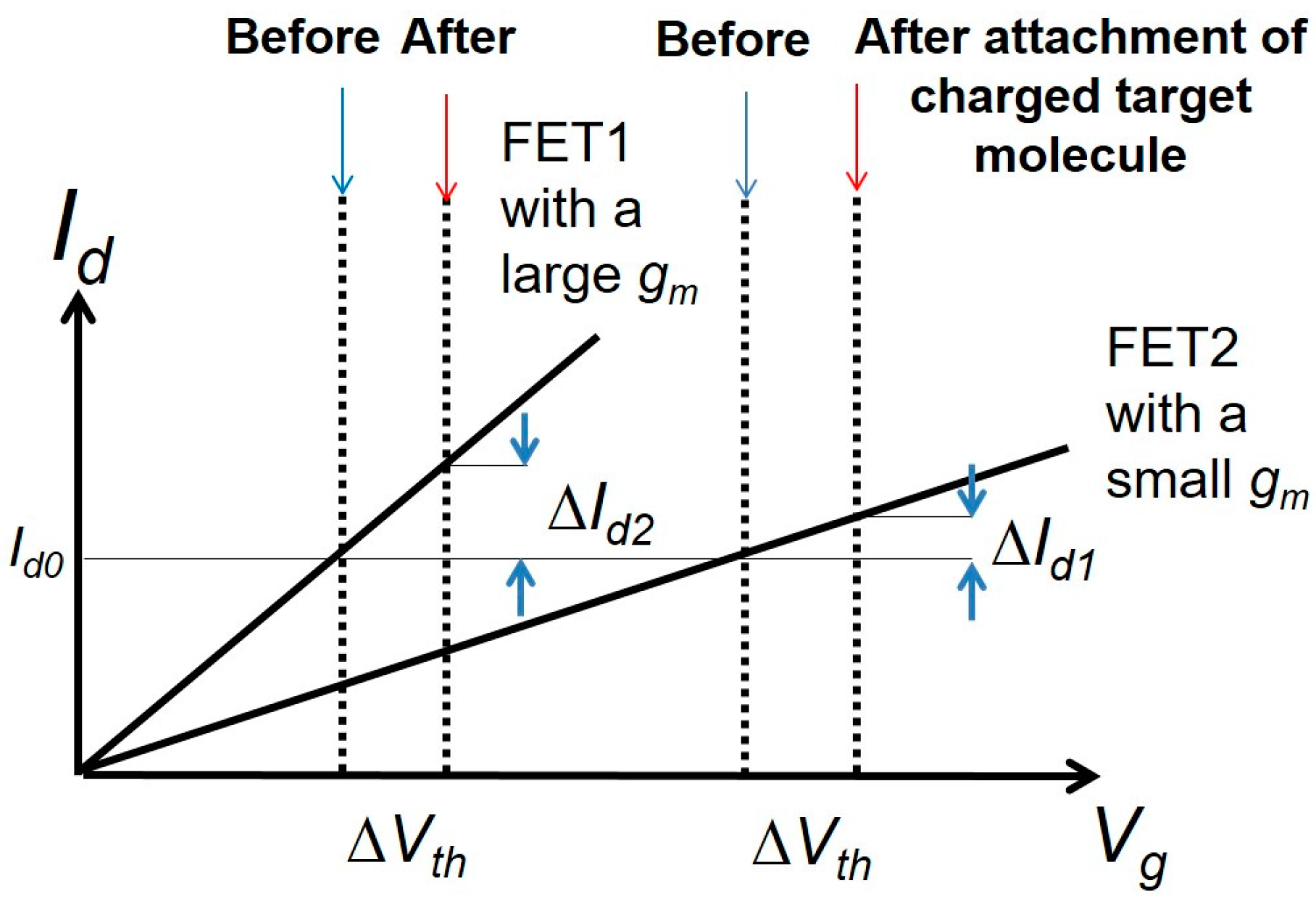
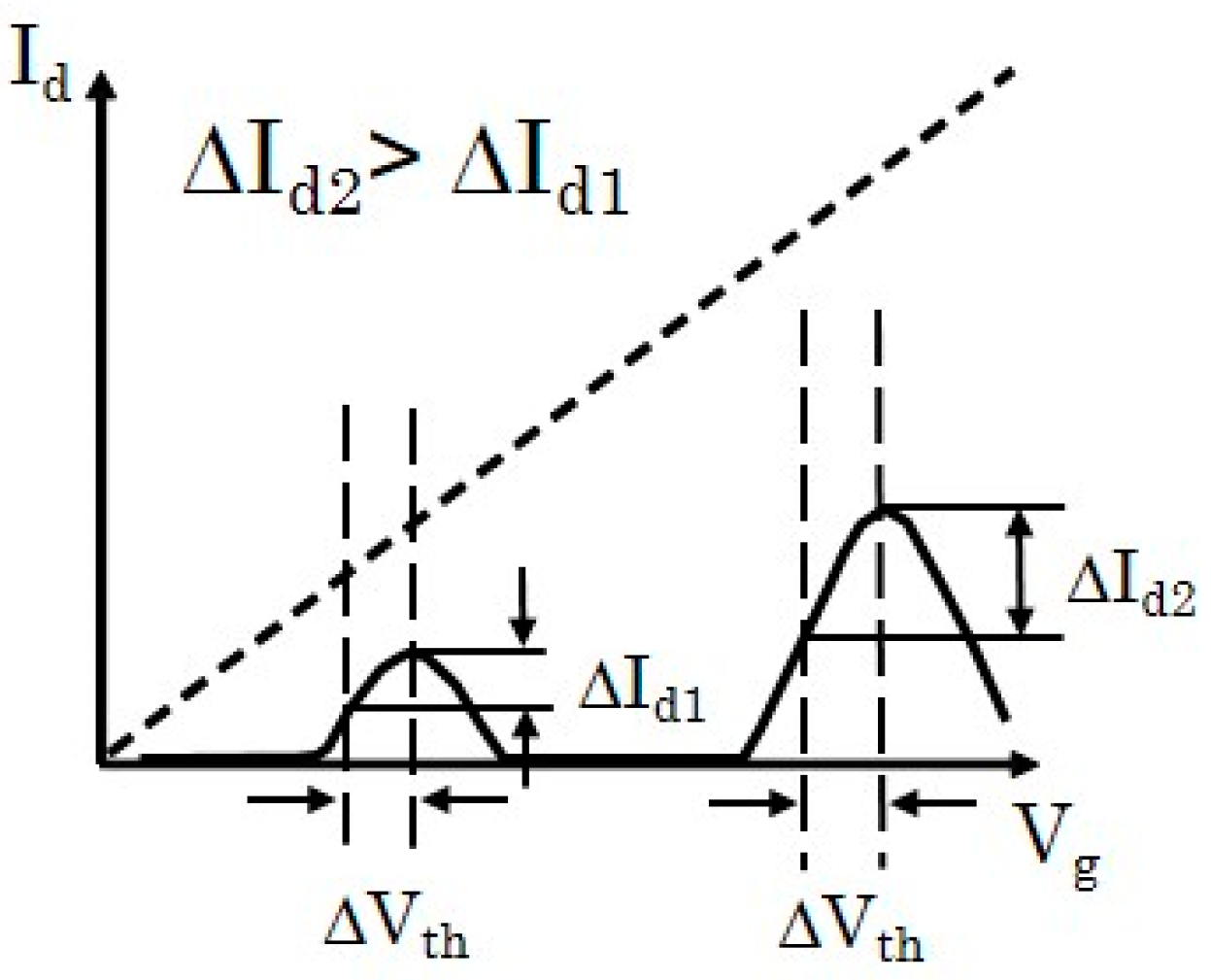
Based on the above consideration, there are two main mechanisms of increase for the detection sensitivity of an FET sensor. One is the increase in transconductance (gm). Since gm is defined as , the FET sensor with a larger gm has a larger magnitude of ΔId (|ΔId|) after the attachment of charged target molecule, as shown in Figure 2. Namely, owing to the larger gm for the FET1 in Figure 2, the magnitude of Id change (|ΔId1|) for the FET1 is larger than that (|ΔId2|) for the FET2.
The other mechanism of the increase in detection sensitivity is the suppression of the effect of percolation for carriers to transfer through the channel in the case of the same polarity of charges between the target molecule and carrier. If the channel width is larger than the size of charged target biomolecule, carriers in the channel can avoid passing through the close region of the target biomolecule and can transfer through the channel; because of this, the percolation path and Id do not change very much from that prior to the attachment. On the other hand, if the channel width is small enough compared with the size of the target biomolecule, carriers cannot avoid passing through the close region of the molecule, leading to the disappearance of the percolation path and large changes to the Id. From the viewpoint of this mechanism, it is effective to decrease the channel width of FET to increase the detection sensitivity. With regard to this percolation effect, the sensitivity enhancement due to the decrease in the channel width of ISFET was confirmed by Monte Carlo simulation [23]. Here, the site percolation property of a finite-size two-dimensional square-lattice system was analyzed to investigate the effect of charged substances on the properties of ISFETs.
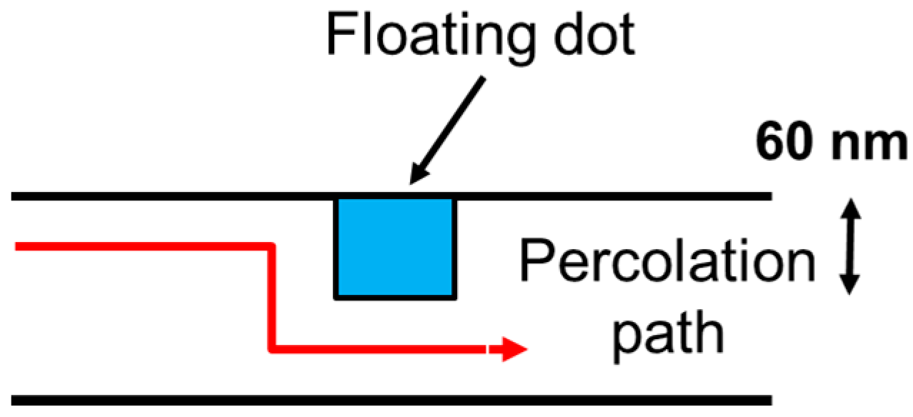
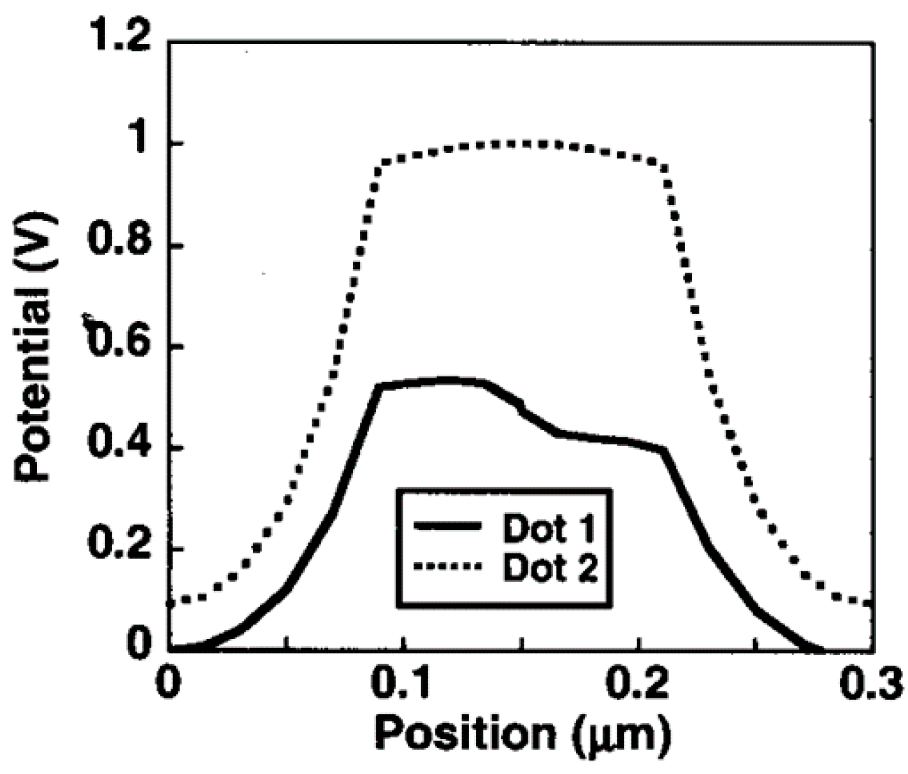
It should be noticed that the operation principle of biosensors with an FET is basically the same as that of floating dot memories, because the attachment of a charged biomolecule on the gate insulator in the biosensors plays the same role as the charge injection of a floating dot in the dot memories. For example, the detection of a biomolecule with an extremely small charge in solution using an FET sensor with a nanowire channel resembles the detection of a single electron injection to a floating dot of the single-electron memory [24,25,26]. The dependence of memory characteristics on the number and distribution of the floating dot were systematically analyzed experimentally and numerically for dots-on-nanowire memories with multiple Si nanoscale floating dots [27,28]. From the numerical results in the case where the width of the channel is wider than the size of the floating dot (Figure 3) [28], the potential in the non-existing region of a floating dot was lower than that in the existing region (Figure 4). This indicates the existence of a percolation path for electrons to pass through the channel when the width of the channel is wider than the size of the dot.
SET sensors should have extremely narrow Si nanowire barriers for the tunnel current to flow at room temperature. The FET sensors used for the comparison with the SET also should have such a narrow nanowire channel region that the tunnel current flows through it, making the percolation effect of carriers well suppressed in this nanowire region.
Because the Coulomb oscillations is modulated and weighted by the current flowing through the nanowire barrier regions, the gm at the corresponding Vg increases with increasing Vg for the SET sensors (Figure 5). Therefore, the gm in the SET sensor can be larger than that in the FET sensor, whose channel consists of the nanowire barrier region, by increasing Vg. Hence, the sensitivity in the SET sensor can be higher than that in the FET sensor with the nanowire channel by increasing Vg.
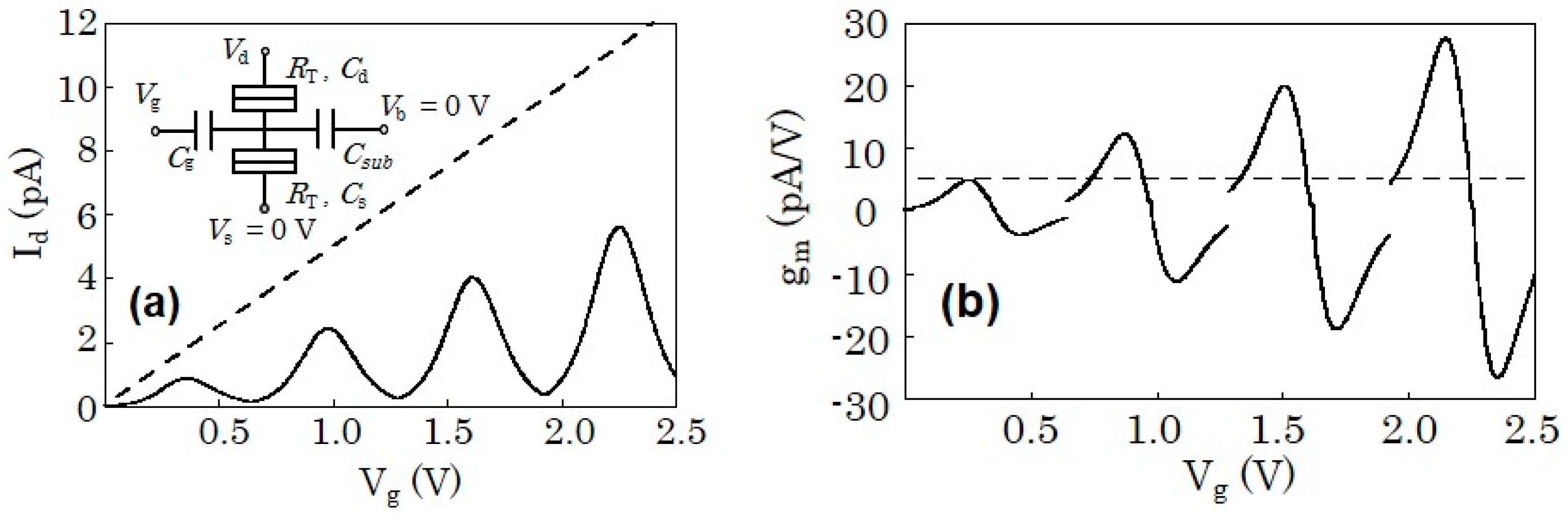
The finding can also be confirmed by the theoretical analysis [22]. The equivalent circuit used for the analysis is shown in the inset of Figure 6. Here, the number of Coulomb islands is assumed to be one, which corresponds to the case where only the smallest island among the multiple islands fabricated acts as a Coulomb island. The Id-Vg characteristics for the SET were calculated using the analytical formula of Id-Vg characteristics for the Coulomb oscillations in the classical regime, weighted by the Vg dependence of current flowing through the nanowire barrier regions. The analytical formula used for Coulomb oscillations is based on the orthodox theory as follows [29,30,31]:
where
where kB, e, T, Vd, Cg, Cs, Cd, Csub, CΣ, and n are the Boltzmann constant, elementary charge, operation temperature, drain voltage, gate capacitance, junction capacitances at source and drain, capacitance between the island and the substrate, total capacitance, and electron number in the Coulomb island. Here, T was set to room temperature. The values of Cg, Cs, and CΣ were obtained from the measurement results of Coulomb oscillations for the SET biosensor in buffer solution [22]. RΣ is the total resistance of the barrier regions, and RΣ = 2RT, where RT is the resistance of a tunnel junction. In the fabricated SET sensors, the buffer solution covers not only Coulomb islands but also the nanowire barrier regions. Since the electric field applied by the voltage of the reference electrode changes the barrier height of the nanowire, the tunnel current through the nanowire junction changes with the voltage. The buffer solution also covers a part of the wide source/drain region and the connecting region between the nanowire barrier region and the source/drain region. The width of the connecting region gradually increased from the nanowire barrier region to the source/drain region in the fabricated devices. These regions act as additional resistance to the tunnel junction resistance in the fabricated SET sensors. If there are only these regions with the additional resistance in the channel of an FET, the analytical formula of the current I can be approximated under the charge-sheet model in the linear region as follows [32]:
where µeff, Cox, W, L, and Vth are the effective mobility, gate oxide capacitance per unit area, effective channel width, effective channel length, and threshold voltage. From the formula, the gm independent of Vg is obtained as
Even if only the tunnel junction resistance is taken into account in the FET, the current through it increases with Vg because the increase in Vg decreases the barrier height. In the calculation of Coulomb oscillations, it was assumed that the current in the tunnel junction increases roughly linearly with Vg because the precise shape of the barrier potential was unclear. Therefore, Vg dependence on RT, including the contribution of the additional resistance, was set so that the current through the junction increases linearly with Vg in the calculation.
The calculated results (solid curves in Figure 6) did, in fact, show the following points: Id at the peaks in Id-Vg characteristics in the SET increases with increasing Vg; the maximum gm values appear at the Vg values near the left-side half maximum of each Id peak. The maximum gm increases with increasing Vg. At large Vg values, the maximum gm values are larger in the case of an SET than the gm in a case where only the nanowire barrier region and the connecting region exist in the channel. In the latter case, the characteristics were calculated for the FET having a nanowire channel with the tunnel junction resistance and the additional resistance (broken curves in Figure 6). It should be noted that the Vg values with the larger gm in the SET can be made to appear near 0 V by adjusting the dopant concentration in the channel and connecting regions. It is also noted that the larger gm values still appear in the case of SET, even if the current through the junction increases with Vg more rapidly than linearly.
The experimental results of Id-Vg characteristics for a fabricated SET biosensor in buffer solution at room temperature confirmed the above results and showed clear Coulomb oscillations in which the peak of Id increases with increasing Vg [22]. Here, Vg was applied by using a reference electrode. This Id increase is due to the increase in the current of the nanowire barrier region with increasing Vg. The corresponding gm-Vg characteristics showed that maximum gm values appear at the Vg values near the left-side half maximum of each Id peak in the Id-Vg characteristics, and that the maximum gm indeed increases with increasing Vg as anticipated above [22].
Finally, it should be noted that if the size of the Coulomb island can be smaller than that in the above-mentioned SET sensor [22], Cg, Cs, Cd, Csub, and CΣ, are smaller in Equations (1) and (2). This leads to a larger gm. Furthermore, an extremely small island size leads to the SET operation in the quantum regime [29,33] from the classical regime. Therefore, the maximum gm of the Coulomb oscillations of the SET can be much larger than that of the corresponding FET with the same nanowire width at the same Vd, even under the constant current through the tunnel junction with increasing Vg.
3. Single-Electron Transistor with Multiple Islands
In the fabricated SET sensors, Si dots were used as Coulomb islands, and the tunnel barriers were formed by the constriction of Si nanowire. The necessary condition for observing single-electron effects, including Coulomb oscillations, is that the charging energy of a Coulomb island should be larger than the energy of operation temperature:
e2/(2CΣ) >> kBT
Consequently, for the room-temperature operation of Si SETs with a single Coulomb island, the island size should be reduced to below 10 nm. In fact, several reports on Si SETs have indicated that the dimension of the Coulomb island should be around 5 nm or below for the room temperature operations [34,35,36], although the precise size to achieve the room temperature SET operation depends on the individual device structure. However, it seems difficult to fabricate such Si SETs with the extremely small Coulomb island reproducibly, even by using current available fabrication techniques. One way to reduce the difficulty is to utilize serially connected islands instead of a single island in the channel region [37]. In such a serially connected multiple-island system, the effective junction capacitance Ceff is smaller than that in a single-island system because the plural junction capacitances are connected in series. In the case of infinite number of serially distributed junction capacitances, for example, the capacitance Ch seen from the edge of a half infinite array is smaller than a junction capacitance C as can be understood from the following relation:
where C0 is a parasitic capacitance including gate and substrate capacitances [38]. The smaller Ceff increases the charging energy e2/(2CΣ) and leads to the increase in the operation temperature. Another reason for the advantage of serially connected islands to the room-temperature SET operation is that it increases the probability of the existence of an extremely small island with an extremely small total capacitance.
With serially connected multiple Coulomb islands, a reliable SET operation is also possible. Generally, in a Coulomb blockade regime, a cotunneling process gives rise to leakage current [39]. The temperature dependence of the valley current of Coulomb oscillations was found to be well described by the inelastic cotunneling theory at high temperatures in the low Vd region [40]. Since the inelastic cotunneling current can be suppressed by multiplexing Coulomb islands, SETs with multiple islands are promising for reliable operation [41]. Furthermore, it was theoretically found that periodic Coulomb oscillations appear with the period determined by the average capacitance in the multiple-island system under the small deviation of gate capacitances [42].
Owing to the above advantages in the multiple-island system, the room-temperature operation of an exclusive-or (XOR) circuit [43] and the high-temperature operation of an exclusive-not-or (EXNOR) circuit [44] have been achieved. Therefore, for the SET sensors in this study, serially connected multiple islands were fabricated in the channel region.
4. Fabrication and Structure of Biosensors with a Single-Electron Transistor with Multiple Islands
In the SET biosensors, geometrically defined multiple islands were fabricated using EB lithography. A non-doped channel structure was adopted for pH detection [20], and a highly doped channel structure was adopted to operate in the accumulation mode for the detections of streptavidin and PSA [21,22]. The final thickness of the channel was less than 20 nm. The final island size and nanowire width were less than 20 nm and 10 nm, respectively. The nanowire region (constrict region in the channel) acts as a tunnel barrier due to the quantum size effect. The channel region, including all barriers and islands in the SET, was inside the solution chamber. The length of channel region was 3.0 µm. The diameter of the chamber was 0.5 cm. An Au reference electrode was used to control the Vg of the SET through a buffer solution.
The process flow of the SET fabrication is as follows [20,21,22]. The thickness of the buried oxide on the B-doped (100) silicon-on-insulator (SOI) wafers used was 400 nm. For the SET with a highly doped channel, the doping (n-type) of the top silicon layer was carried out by POCl3 diffusion. The doping level of the channel and source/drain regions was about 3.5 × 1020 cm−3. For the SET with a non-doped channel, no channel doping was performed. The fabrication process of a channel region includes EB lithography and dry etching. Subsequent isotropic wet etching in a solution of NH4OH/H2O2/H2O reduced the dimension of the channel and the damage introduced during the dry etching process [45]. The numbers of island were 11. Smaller numbers of island tended to increase the island size due to the proximity effect of the wide source/drain region in the EB lithography. Larger numbers of island, on the other hand, tended to increase the probability of disconnection in the nanowire barrier region. For the SET with a non-doped channel, the source and drain areas were formed by ion implantation of As+. Then, a Si3N4/SiO2 stacked gate insulator was fabricated: A layer of SiO2, about 10 nm thick, was thermally grown, followed by the deposition of about 90-nm-thick Si3N4 by low-pressure chemical vapor deposition. This Si3N4 layer prevents the invasion of ions such as Na+ and K+ from the buffer solution into the inside of gate insulator, and enables reliable SET operation. After contact holes and Al electrodes were fabricated, the samples were annealed at 400 °C in an H2 atmosphere. Then, a solution chamber or a fluidic channel was attached to the Si3N4/SiO2 gate insulator.
5. Experimental Demonstrations of Biomolecule Sensing Based on a Single-Electron Transistor
Using the biosensors with an SET that has serially connected multiple Si islands, pH sensor and detections of streptavidin and PSA have been achieved.
5.1. Ion (pH) Detection
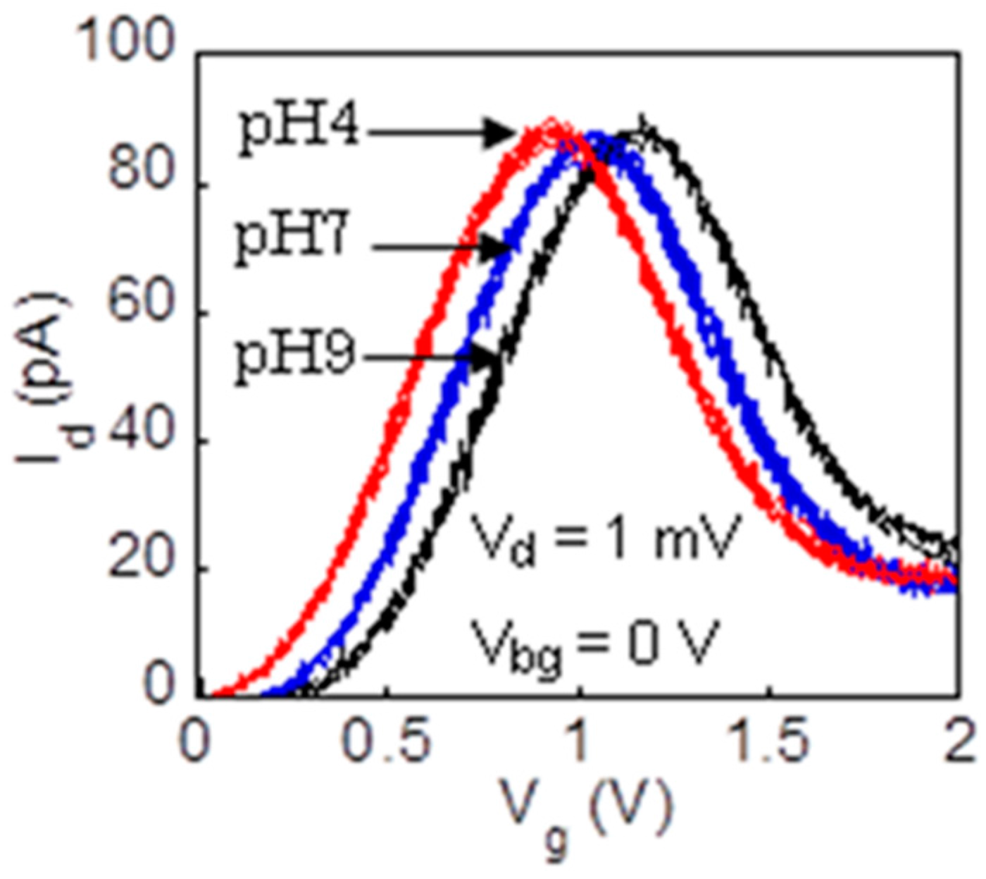
For the pH detection [20], the Id-Vg characteristics were measured for three different buffer solutions: 50 mM phthalate, pH 4; 50 mM phosphate, pH 7; and 10 mM tetraborate, pH 9 (Figure 8). The reference electrode in the buffer solutions was used as a gate. With the increasing pH, the Id-Vg curve shifted toward the high Vg side. Both in the increase and decrease in pH, the positions of Id-Vg curves for the same pH coincide well. Therefore, a reproducible pH response was observed using an SET biosensor for the first time.
5.2. Detection of Streptavidin
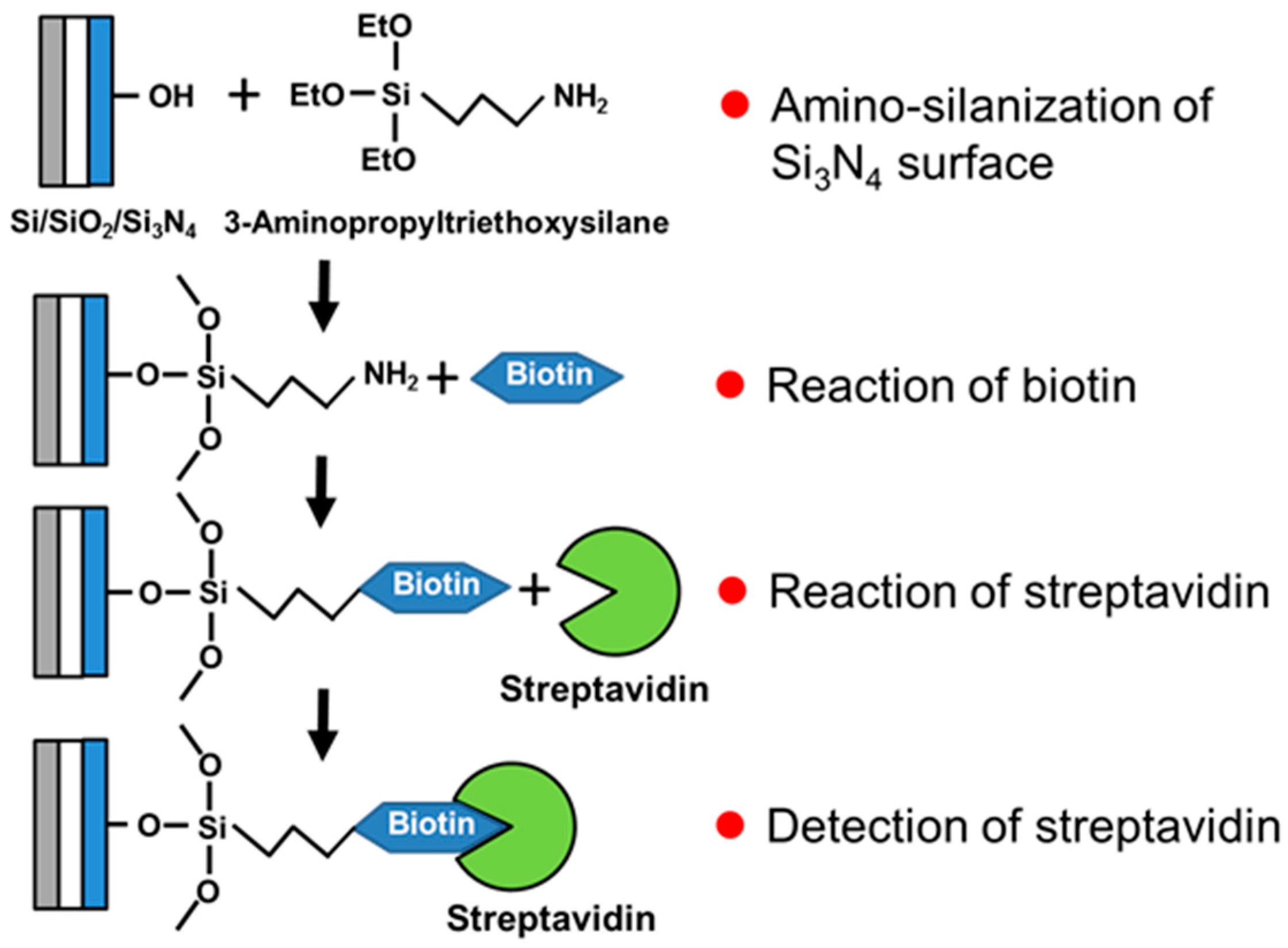
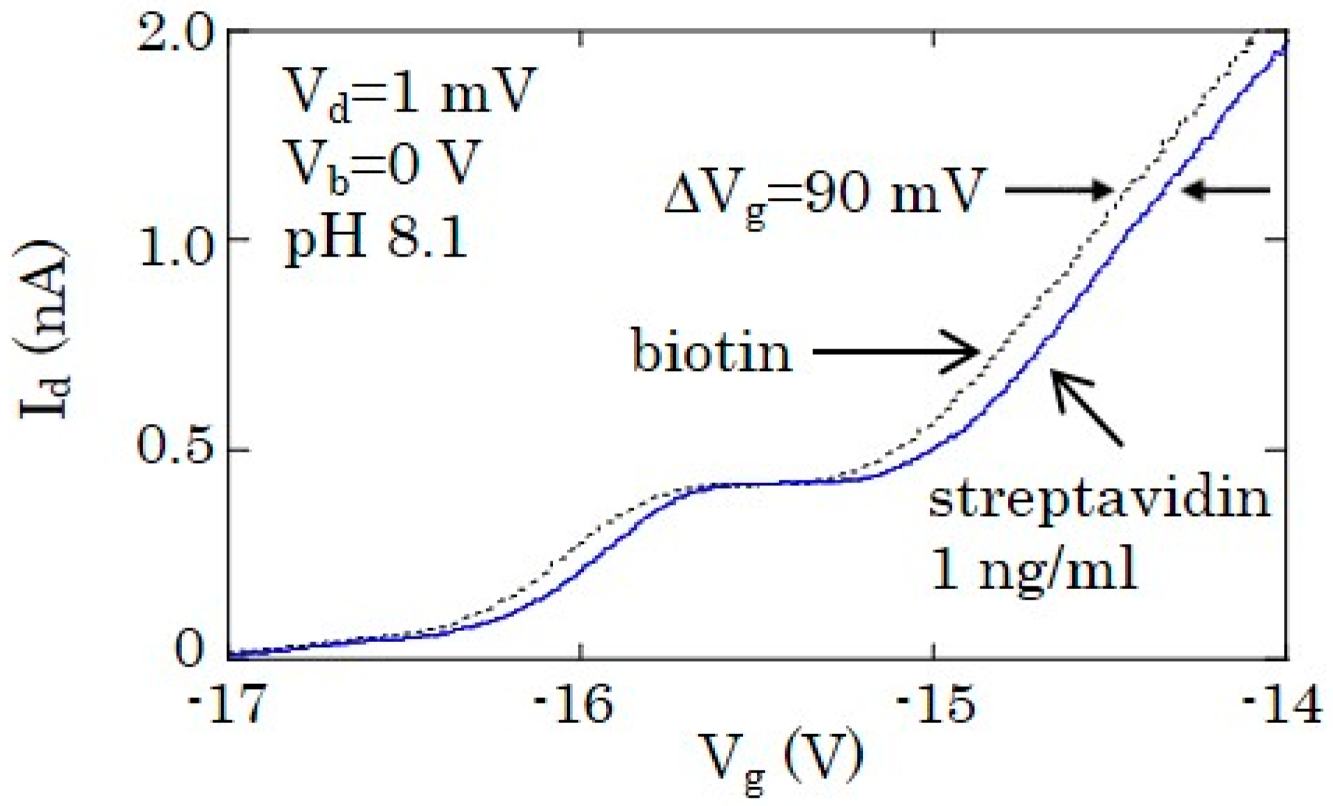
For the detection of streptavidin, a well-known ligand-receptor binding of biotin-streptavidin was used. Therefore, before the introduction of the target biomolecule (streptavidin), the corresponding receptor (biotin) had to be coupled to the surface of the gate insulator of the SET sensor. Then, the target biomolecules of streptavidin were introduced. After the ligand-receptor binding, the charge on the surface of gate insulator changed the electrical characteristics of the sensor. Figure 9 shows the surface modification of the gate insulator for the detection of streptavidin. After the silicon nitride surface was cleaned and amino-silanized, biotin was reacted with the surface. Then, the biotinylated surface was reacted with streptavidin. Negative Vg shift (ΔVg) of the Id-Vg curve of Coulomb oscillations was observed after the attachment of biotin to the surface of the gate insulator [21]. The successive addition of streptavidin resulted in a positive ΔVg, which was consistent with the negative charge of streptavidin in solution at pH 8.0–8.2. Therefore, biomolecule detection using an SET sensor was achieved for the first time [21]. The concentration of streptavidin was 10 µg/mL in the above measurement. Later, the detection of streptavidin binding down to 1 ng/mL (16 pM) was achieved (Figure 10) using an SET sensor [22].
5.3. Detection of PSA
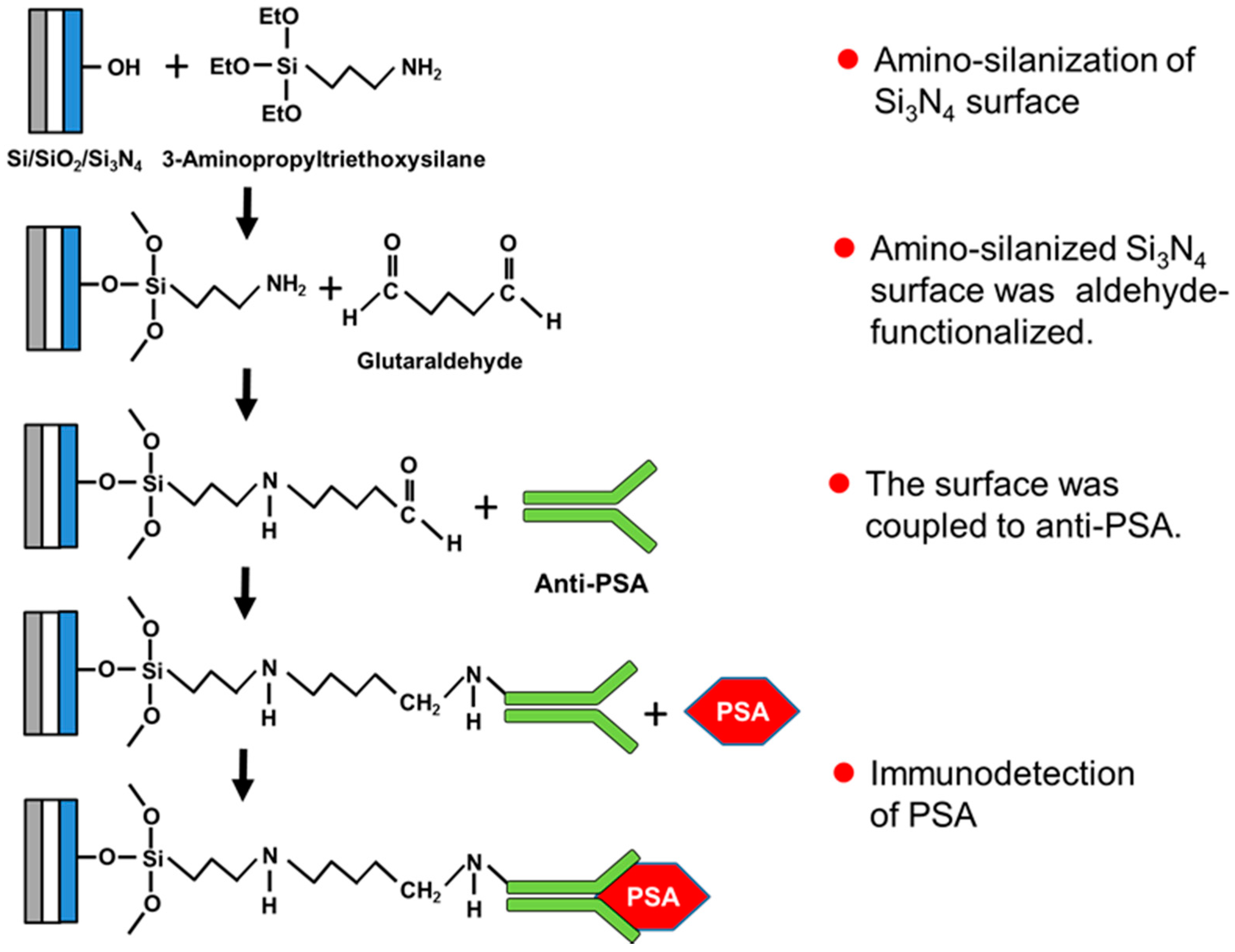
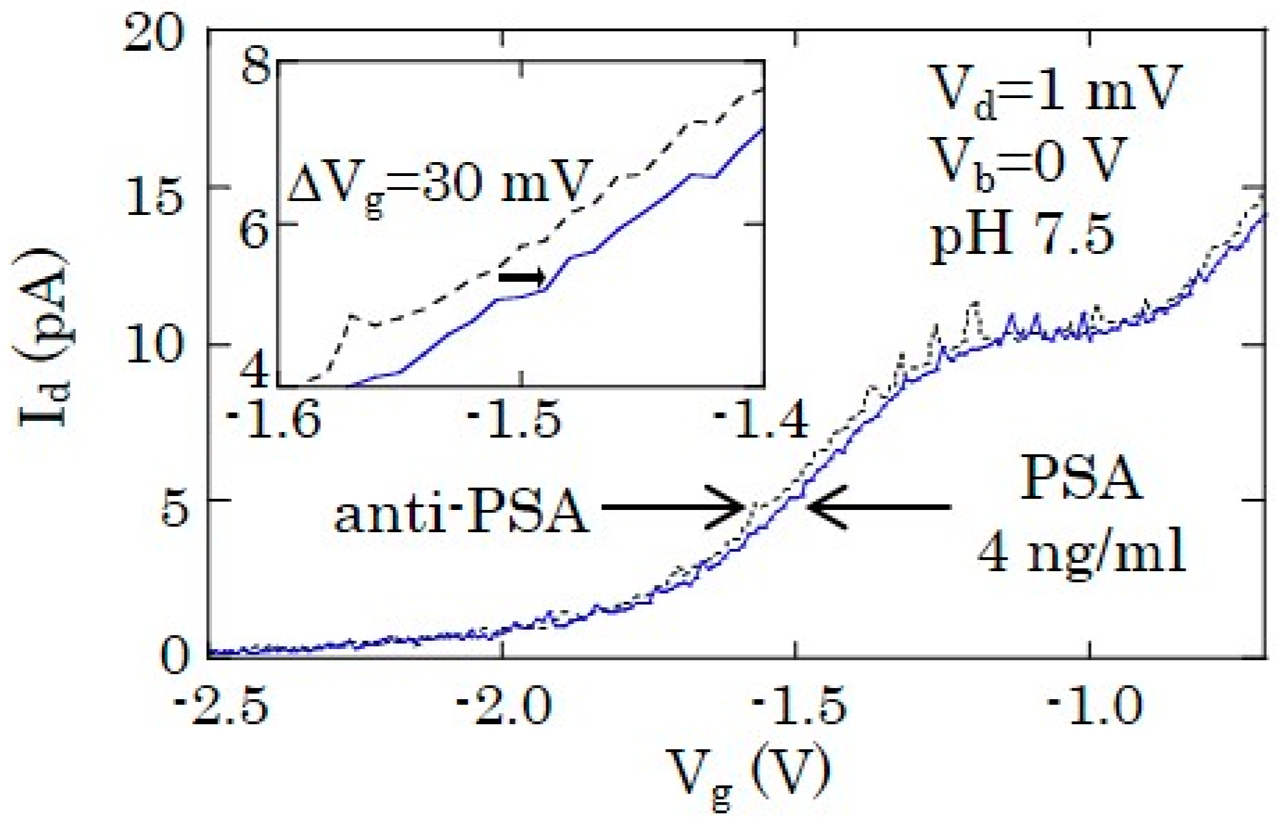
The immunodetection of PSA has been achieved using an SET sensor [22]. The surface modification of the gate insulator was carried out as follows (Figure 11). After silicon nitride surface was anino-silanized, the surface was aldehyde-functionalized. Then, the surface was coupled to the antibody of PSA (anti-PSA). The immunodetection of PSA can be carried out using the specific binding of the antigen and antibody.
For the binding event of 4 ng/mL of PSA to anti-PSA, a positive ΔVg of 30 mV was observed (Figure 12). The positive ΔVg is consistent with the negative charge of PSA in solution at pH 7.5 due to the isoelectric point (6.9) of PSA. It should be noted that 4 ng/mL is the required detection level for practical use because this is the cut-off value for the precise inspection of prostate cancer.
6. Summary and Future Perspectives
In this review, the feasibility of the ultrahigh-sensitive detection of ions and biomolecules using a Si SET biosensor was clearly proven through systematic study. Silicon structures are important for large-scale integration of SET sensors and the peripheral circuits. The mechanism for the ultrahigh-sensitive detection of ions/biomolecules based on an SET sensor was explained and compared with the detection mechanism using a nanowire FET sensor. Nanowire FET sensors can decrease the percolation effect by decreasing the channel width; however, it cannot increase gm because of the narrowness of the channel width. On the other hand, SET sensors can increase gm while keeping the channel width narrow, which leads to a decrease in the percolation effect. This was confirmed by theoretical and experimental analyses. Therefore, in principle, the sensitivity in an SET sensor can be made higher than that in a nanowire FET sensor by increasing Vg. Here, the Vg values with the larger gm in the SET can be made to appear near 0 V by adjusting the dopant concentration in the channel and the connecting regions between the channel and the source/drain.
From the requirement for room-temperature SET operation, the width of the island must be around 10 nm or less. SET biosensors have the clear advantage over nanowire FET biosensors in detecting the biomolecules with a size of around 10 nm or less. In the detection of biomolecules much larger than 10 nm, highly sensitive detection also can be carried out by using the nanowire FET sensor with a large channel width (the same width as the size of the biomolecule), because the gm of such FET sensors are very large. In contrast, nanowire barriers with a large width cannot be used for an SET in the detection of biomolecules much larger than 10 nm, because the quantum confinement effect does not occur and room-temperature SET operations are not possible with such wide nanowire barriers. Consequently, the gm of an SET cannot be increased by enlarging the width of nanowire barrier when detecting biomolecules much larger than 10 nm. The only means of increasing the gm of the SET in this case is to increase Vg. By increasing Vg, the resistance of nanowire barrier decreases. This leads to an increase in the current flowing in the nanowire barriers and the gm of SET. However, there is an upper limit of Vg applied for SET operation. When the resistance of a nanowire barrier becomes smaller than the resistance quantum (25.813 kΩ) by increasing Vg, the quantum fluctuation in the electron number in the island due to tunneling through the barrier becomes large, and this makes SET operation impossible [29]. Therefore, nanowire FET biosensors have greater sensitivity than SET biosensors in detecting extremely large biomolecules. However, even in this case, the actual size of the biomolecule may be much smaller than its nominal size due to the Debye shielding in the solution, which may make the sensitivity of SET greater. Experimental and theoretical research is necessary to clarify this.
The room-temperature operation of Si SETs is inevitably necessary for ion sensors and biosensors because these sensors use buffer solutions. Because a serially connected multiple-island channel structure is advantageous to room-temperature operation of SET, a pH sensor and biomolecule sensors for the detection of streptavidin have been developed based on the SETs with the channel structure. The detection of PSA at the cut-off concentration (4 ng/mL) has been also achieved by the SET sensor, which leads to practical use.
One significant problem in achieving the integration of ultrahigh-sensitive SET sensors is that it is difficult to obtain the uniform Id-Vg characteristics for the plural SETs, although room-temperature SET operation can be possible. Since the island size has to be on the order of 10 nm, simply by adopting the multiple-island channel structure for room-temperature SET operation, a size fluctuation of only a few nm leads to quite different Id-Vg characteristics for the SET, which will make it difficult to integrate the sensors. More precise control of the size of the channel structure is necessary by refining the EB lithography or dry etching technique, although it would be very difficult to avoid the problem of line edge roughness for thin and long Si wire structures. A combination of the EB lithography technique and the self-limiting or assembling technique is another possible way to obtain reliable room-temperature SET operation. For example, Shin et al. reported the room-temperature operation of an SET with a Coulomb island less than 5 nm in size that was fabricated by combining the EB lithography with the pattern-dependent oxidation of Si nanowire [34]. By overcoming such problems, Si SET biosensors will open the door to an integrated single-chip sensor system suitable for multiplexed and simultaneous diagnoses with ultrahigh sensitivity.
Acknowledgments
This study was supported in part by a Grant-Aid for Scientific Research (B) (Grant No. 25289103) from Japan Society for the Promotion of Science.
Conflicts of Interest
The author declares no conflict of interest.
References
- Bergveld, P. Development, operation, and application of the ion-sensitive field-effect transistor as a tool for electrophysiology. IEEE Trans. Biomed. Eng. 1972, BME-19, 342–351. [Google Scholar] [CrossRef] [PubMed]
- Gotoh, M.; Tamiya, E.; Karube, I.; Kagawa, Y. A microsensors for adenosine-5′-triphosphate pH-sensitive field effect transistors. Anal. Chim. Acta 1986, 187, 287–291. [Google Scholar] [CrossRef]
- Park, K.; Kim, M.; Choi, S. Fabrication and characteristics of MOSFET protein chip for detection of ribosomal protein. Biosens. Bioelectron. 2005, 20, 2111–2115. [Google Scholar] [CrossRef] [PubMed]
- Kim, D.; Jeong, Y.; Park, H.; Shin, J.; Choi, P.; Lee, J.; Lim, G. An FET-type charge sensor for highly sensitive detection of DNA sequence. Biosens. Bioelectron. 2004, 20, 69–74. [Google Scholar] [CrossRef] [PubMed]
- Sakata, T.; Kamahori, M.; Miyahara, Y. DNA analysis chip based on field-effect transistors. Jpn. J. Appl. Phys. 2005, 44, 2854–2859. [Google Scholar] [CrossRef]
- Mohanty, N.; Berry, V. Graphene-based single-bacterium resolution biodevice and DNA transistor: Interfacing graphene derivatives with nanoscale and microscale biocomponents. Nano Lett. 2008, 8, 4469–4476. [Google Scholar] [CrossRef] [PubMed]
- Ohno, Y.; Maehashi, K.; Yamashiro, Y.; Matsumoto, K. Electrolyte-gated graphene field-effect transistors for detecting pH and protein adsorption. Nano Lett. 2009, 9, 3318–3322. [Google Scholar] [CrossRef] [PubMed]
- Khan, H.U.; Roberts, M.E.; Johnson, O.; Förch, R.; Knoll, W.; Bao, Z. In Situ, label-free DNA detection using organic transistor sensors. Adv. Mater. 2010, 22, 4452–4456. [Google Scholar] [CrossRef] [PubMed]
- Cui, Y.; Wei, Q.; Park, H.; Lieber, C.M. Nanowire nanosensors for highly sensitive and selective detection of biological and chemical species. Science 2001, 293, 1289–1292. [Google Scholar] [CrossRef] [PubMed]
- Patolsky, F.; Zheng, G.; Hayden, O.; Lakadamyali, M.; Zhuang, X.; Lieber, C.M. Electrical detection of single viruses. Proc. Natl. Acad. Sci. USA 2004, 101, 14017–14022. [Google Scholar] [CrossRef] [PubMed]
- Wang, W.U.; Chen, C.; Lin, K.; Fang, Y.; Lieber, C.M. Label-free detection of small-molecule-protein interactions by using nanowire nanosensors. Proc. Natl. Acad. Sci. USA 2005, 102, 3208–3212. [Google Scholar] [CrossRef] [PubMed]
- Zheng, G.; Patolsky, F.; Cui, Y.; Wang, W.U.; Lieber, C.M. Multiplexed electrical detection of cancer markers with nanowire sensor arrays. Nat. Biotechnol. 2005, 23, 1294–1301. [Google Scholar] [CrossRef] [PubMed]
- Stern, E.; Klemic, J.F.; Routenberg, D.A.; Wyrembak, P.N.; Turner-Evans, D.B.; Hamilton, A.D.; LaVan, D.A.; Fahmy, T.M.; Reed, M.A. Label-free immunodetection with CMOS-compatible semiconducting nanowires. Nature 2007, 445, 519–522. [Google Scholar] [CrossRef] [PubMed]
- Li, Z.; Chen, Y.; Li, X.; Kamins, T.I.; Nauka, K.; Williams, R.S. Sequence-specific label-free DNA sensors based on silicon nanowires. Nano Lett. 2004, 4, 245–247. [Google Scholar] [CrossRef]
- Kim, A.; Ah, C.S.; Yu, H.Y.; Yang, J.; Baek, I.; Ahn, C.; Park, C.W.; Jun, M.S. Ultrasensitive, label-free, and real-time immunodetection using silicon field-effect transistors. Appl. Phys. Lett. 2007, 91. [Google Scholar] [CrossRef]
- Kudo, T.; Kasama, T.; Ikeda, T.; Hata, Y.; Tokonami, S.; Yokoyama, S.; Kikkawa, T.; Sunami, H.; Ishikawa, T.; Suzuki, M.; et al. Fabrication of Si nanowire field-effect transistor for highly sensitive, label-free biosensing. Jpn. J. Appl. Phys. 2009, 48. [Google Scholar] [CrossRef]
- Knopfmacher, O.; Tarasov, A.; Fu, W.; Wipf, M.; Niesen, B.; Calame, M.; Schönenberger, C. Nernst limit in dual-gated Si-nanowire FET sensors. Nano Lett. 2010, 10, 2268–2274. [Google Scholar] [CrossRef] [PubMed]
- Chen, R.J.; Bangsaruntip, S.; Drouvalakis, K.A.; Kam, N.W.S.; Shim, M.; Li, Y.; Kim, W.; Utz, P.J.; Dai, H. Noncovalent functionalization of carbon nanotubes for highly specific electronic biosensors. Proc. Natl. Acad. Sci. USA 2003, 100, 4984–4989. [Google Scholar] [CrossRef] [PubMed]
- Maehashi, K.; Katsura, T.; Kerman, K.; Takamura, Y.; Matsumoto, K.; Tamiya, E. Label-free protein biosensor based on aptamer-modified carbon nanotube field-effect transistors. Anal. Chem. 2007, 79, 782–787. [Google Scholar] [CrossRef] [PubMed]
- Kudo, T.; Nakajima, A. Highly sensitive ion detection using Si single-electron transistors. Appl. Phys. Lett. 2011, 98. [Google Scholar] [CrossRef]
- Kudo, T.; Nakajima, A. Biomolecule detection based on Si single-electron transistors for highly sensitive integrated sensors on a single chip. Appl. Phys. Lett. 2012, 100. [Google Scholar] [CrossRef]
- Nakajima, A.; Kudo, T.; Furuse, S. Biomolecule detection based on Si single-electron transistors for practical use. Appl. Phys. Lett. 2013, 103. [Google Scholar] [CrossRef]
- Kasama, T.; Nakajima, A. Monte carlo simulation of the two-dimensional site percolation problem for designing sensitive and quantitatively analyzable field-effect transistors. Jpn. J. Appl. Phys. 2009, 48. [Google Scholar] [CrossRef]
- Nakajima, A.; Futatsugi, T.; Kosemura, K.; Fukano, T.; Yokoyama, N. Room temperature operation of Si single-electron memory with self-aligned floating dot gate. Appl. Phys. Lett. 1997, 70, 1742–1744. [Google Scholar] [CrossRef]
- Nakajima, A.; Futatsugi, T.; Kosemura, K.; Fukano, T.; Yokoyama, N. Si single electron tunneling transistor with nanoscale floating dot stacked on a Coulomb island by self-aligned process. Appl. Phys. Lett. 1997, 71, 353–355. [Google Scholar] [CrossRef]
- Nakajima, A.; Futatsugi, T.; Kosemura, K.; Fukano, T.; Yokoyama, N. Si single-electron tunneling transistor with nanoscale floating dot stacked on a Coulomb island by self-aligned process. J. Vac. Sci. Technol. B 1999, 17, 2163–2172. [Google Scholar] [CrossRef]
- Nakajima, A.; Fujiaki, T.; Fukuda, Y. Dependence of charge storage and programming characteristics on dot number of floating dot memory. Appl. Phys. Lett. 2008, 92. [Google Scholar] [CrossRef]
- Nakajima, A.; Fujiaki, T.; Ezaki, T. Impact of floating dot distribution on memory characteristics of self-aligned dots-on nanowire memory. J. Appl. Phys. 2009, 105. [Google Scholar] [CrossRef]
- Kouwenhoven, L.P.; McEuen, P.L. Single electron transport through a quantum dot. In Nanotechnology; Timp, G., Ed.; Springer: New York, NY, USA, 1998; pp. 471–535. [Google Scholar]
- Uchida, K.; Matsuzawa, K.; Koga, J.; Ohba, R.; Takagi, S.; Toriumi, A. Analytical single-electron transistor (SET) model for design and analysis of realistic SET circuits. Jpn. J. Appl. Phys. 2000, 39, 2321–2324. [Google Scholar] [CrossRef]
- Inokawa, H.; Takahashi, Y. A compact analytical model for asymmetric single-electron tunneling transistors. IEEE Trans. Electron Devices 2003, 50, 455–461. [Google Scholar] [CrossRef]
- Taur, Y.; Ning, T.H. Fundamenatals of Modern VLSI Devices; The Press Syndicate of the University of Cambridge: Cambridge, UK, 1998; pp. 118–119. [Google Scholar]
- Beenakker, C.W.J. Theory of Coulomb-blockade oscillations in the conductance of a quantum dot. Phys. Rev. B 1991, 44, 1646–1656. [Google Scholar] [CrossRef]
- Shin, S.J.; Jung, C.S.; Park, B.J.; Yoon, T.K.; Lee, J.J.; Kim, S.J.; Choi, J.B.; Takahashi, Y.; Hasko, D.G. Si-based ultrasmall multiswitching single-electron transistor operating at room-temperature. Appl. Phys. Lett. 2010, 97. [Google Scholar] [CrossRef]
- Shin, S.J.; Lee, J.J.; Kang, H.J.; Choi, J.B.; Yang, S.E.; Takahashi, Y.; Hasko, D.G. Room-temperature charge stability modulated by quantum effects in a nanoscale silicon island. Nano Lett. 2011, 11, 1591–1597. [Google Scholar] [CrossRef] [PubMed]
- Lavieville, R.; Triozon, F.; Barraud, S.; Corna, A.; Jehl, X.; Sanquer, M.; Li, J.; Abisset, A.; Duchemin, I.; Niquet, Y. Quantum dot made in metal oxide silicon-nanowire field effect transistor working at room temperature. Nano Lett. 2015, 15, 2958–2964. [Google Scholar] [CrossRef] [PubMed]
- Nakajima, A.; Ito, Y.; Yokoyama, S. Conduction mechanism of Si single-electron transistor having a one-dimensional regular array of multiple tunnel junctions. Appl. Phys. Lett. 2002, 81, 733–735. [Google Scholar] [CrossRef]
- Delsing, P. One-dimensional arrays of small tunnel junctions. In Single Charge Tunneling, Coulomb Blockade Phenomena in Nanostructures; Grabert, H., Devoret, M.H., Eds.; NATO ASI Series B 294; Plenum: New York, NY, USA, 1992; pp. 249–274. [Google Scholar]
- Takahashi, Y.; Horiguchi, S.; Fujiwara, A.; Murase, K. Co-tunneling current in very small Si single-electron transistors. Phys. B 1996, 227, 105–108. [Google Scholar] [CrossRef]
- Ohkura, K.; Kitade, T.; Nakajima, A. Cotunneling current in Si single-electron transistor based on multiple islands. Appl. Phys. Lett. 2006, 89. [Google Scholar] [CrossRef]
- Ohkura, K.; Kitade, T.; Nakajima, A. Electrical characteristics of Si single-electron transistor based on multiple Islands. Jpn. J. Appl. Phys. 2007, 46, 6233–6236. [Google Scholar] [CrossRef]
- Ohkura, K.; Kitade, T.; Nakajima, A. Periodic Coulomb oscillations in Si single-electron transistor based on multiple islands. J. Appl. Phys. 2005, 98. [Google Scholar] [CrossRef]
- Kitade, T.; Ohkura, K.; Nakajima, A. Room-temperature operation of an exclusive-OR circuit using a highly doped Si single-electron transistor. Appl. Phys. Lett. 2005, 86. [Google Scholar] [CrossRef]
- Kitade, T.; Nakajima, A. Application of highly doped Si single-electron transistors to an exclusive-NOR operation. Jpn. J. Appl. Phys. 2004, 43, L418–L420. [Google Scholar] [CrossRef]
- Nakajima, A.; Aoyama, H.; Kawamura, K. Isolated nanometer-size Si dot arrays fabricated using electron-beam lithography, reactive ion etching, and wet etching in NH4OH/H2O2/H2O. Jpn. J. Appl. Phys. 1994, 33, L1796–L1798. [Google Scholar] [CrossRef]
Figure 1.
Drain current (Id) versus gate voltage (Vg) characteristics of a field effect transistor before and after the attachment of charged biomolecule. Id changes from an on-current state (Id0) to an off-current state at the same Vg (Vg0) by the threshold voltage shift (ΔVth).
Figure 1.
Drain current (Id) versus gate voltage (Vg) characteristics of a field effect transistor before and after the attachment of charged biomolecule. Id changes from an on-current state (Id0) to an off-current state at the same Vg (Vg0) by the threshold voltage shift (ΔVth).

Figure 2.
Schematic view to explain that the sensor that has a field effect transistor (FET) with a larger transconductance (gm) has a larger magnitude of the change in drain current Id (ΔId) after the attachment of charged target molecule. Owing to the larger gm for the FET1, the magnitude of ΔId for the FET1 (|ΔId1|) is larger than that for the FET2 (|ΔId2|). ΔVth is the threshold voltage shift after the attachment of charged target.

Figure 3.
Schematic view of dot distribution in a dots-on-nanowire memory with one Si nanoscale floating dot whose width is smaller than that of the channel.
Figure 3.
Schematic view of dot distribution in a dots-on-nanowire memory with one Si nanoscale floating dot whose width is smaller than that of the channel.

Figure 4.
Calculated potential profile perpendicular to the current direction for dots-on-nanowire memories with single and double Si floating dots. Schematic distribution of the single dot is shown in Figure 3. Reproduced with permission from [28], Copyright 2009, AIP Publishing LLC.

Figure 5.
Schematic view of Id–Vg characteristics for the sensor with a single-electron transistor. ΔVth is the threshold voltage shift after the attachment of a charged target. ΔVth is the threshold voltage shift after the attachment of a charged target. ΔId1 and ΔId2 are the change in Id at different Vg values after the attachment. Reproduced with permission from [22], Copyright 2013, AIP publishing LLC.

Figure 6.
(a) Analytical drain current (Id)-gate voltage (Vg) characteristics of a single-electron transistor (SET) (solid curve). The inset shows the equivalent circuit used for the calculation. The broken curve is the analytical Id-Vg characteristics when only the nanowire barrier region exists in the channel; (b) Analytical transconductance (gm)-Vg characteristics of an SET (solid curve). The broken curve is the analytical gm-Vg characteristics when only the nanowire barrier region exists in the channel. Reproduced with permission from [22], Copyright 2013, AIP Publishing LLC.

Figure 7.
Contour plot of drain current Id as a function of drain voltage (Vd) and back-gate voltage (Vbg) at room temperature. Reproduced with permission from [20], Copyright 2011, AIP Publishing LLC.
Figure 7.
Contour plot of drain current Id as a function of drain voltage (Vd) and back-gate voltage (Vbg) at room temperature. Reproduced with permission from [20], Copyright 2011, AIP Publishing LLC.

Figure 8.
Drain current (Id)-gate voltage (Vg) characteristics of an SET sensor for three different pH values at room temperature. Reproduced with permission from [20], Copyright 2011, AIP Publishing LLC.
Figure 8.
Drain current (Id)-gate voltage (Vg) characteristics of an SET sensor for three different pH values at room temperature. Reproduced with permission from [20], Copyright 2011, AIP Publishing LLC.

Figure 9.
Surface modification of the gate insulator for the detection of streptavidin.

Figure 10.
Drain current (Id)-gate voltage (Vg) characteristics of an SET sensor for the detection of streptavidin. Reproduced with permission from [22], Copyright 2013, AIP Publishing LLC.
Figure 10.
Drain current (Id)-gate voltage (Vg) characteristics of an SET sensor for the detection of streptavidin. Reproduced with permission from [22], Copyright 2013, AIP Publishing LLC.

Figure 11.
Surface modification of the gate insulator for the detection of prostate specific antigen (PSA).
Figure 11.
Surface modification of the gate insulator for the detection of prostate specific antigen (PSA).

Figure 12.
Drain current (Id)-gate voltage (Vg) characteristics of an SET sensor for the detection of PSA. Reproduced with permission from [22], Copyright 2013, AIP Publishing LLC.
Figure 12.
Drain current (Id)-gate voltage (Vg) characteristics of an SET sensor for the detection of PSA. Reproduced with permission from [22], Copyright 2013, AIP Publishing LLC.

© 2016 by the author; licensee MDPI, Basel, Switzerland. This article is an open access article distributed under the terms and conditions of the Creative Commons by Attribution (CC-BY) license (http://creativecommons.org/licenses/by/4.0/).
Share and Cite
MDPI and ACS Style
Nakajima, A. Application of Single-Electron Transistor to Biomolecule and Ion Sensors. Appl. Sci. 2016, 6, 94. https://doi.org/10.3390/app6040094
AMA Style
Nakajima A. Application of Single-Electron Transistor to Biomolecule and Ion Sensors. Applied Sciences. 2016; 6(4):94. https://doi.org/10.3390/app6040094
Chicago/Turabian StyleNakajima, Anri. 2016. "Application of Single-Electron Transistor to Biomolecule and Ion Sensors" Applied Sciences 6, no. 4: 94. https://doi.org/10.3390/app6040094
Note that from the first issue of 2016, this journal uses article numbers instead of page numbers. See further details here.