
Abstract
The electrical and electroluminescent properties of MOVPE GaN p-n homojunctions have been analyzed as a function of temperature and bias. Electroluminescence is observed for V>3 V under dc and ac conditions. The main emission at low T is a donor-acceptor transition involving shallow acceptors, though it disappears at higher T due to the ionization of the acceptors and compensation by ionized donors. Room temperature dc and ac electroluminescence spectra evolve under increasing bias from a blue-shifting visible band involving deep states at the p-type side of the p-n junction, to a band-to-band UV recombination at high bias. In agreement, the superlinear dependence of light-current characteristics at low current injection becomes linear when the defects are saturated. Time analysis of the spectra vs pulse duration and duty cycle allows the determination of the visible radiative recombination and relaxation times associated to the Mg-related deep states, which are found to behave as acceptors lying 0.55 eV above the valence band. A simple 3-level model is able to explain the visible emission, which involves the conduction band (or shallow donor) and those deep acceptors in the p-layer. Optimum UV/visible ratio emission requires intense and relatively long pulses, with a high duty cycle to impede visible recombination.
1. Introduction
Recently, an impressive progress in wide band-gap III-nitride research has led to the succesful development of blue light-emitting diodes (LEDs) and lasers [1] [2]. These realisations have been possible because of the improved crystal quality obtained by Metal Organics Vapor Phase Epitaxy (MOVPE), and especially because of the achievement of GaN p-type doping. Improved growth process (use of buffer layers, purification of carrier gases, and so on) have allowed the reduction of the electron residual concentration.
The mechanism of acceptor compensation which prevents obtaining low resistivity GaN:Mg by MOVPE is likely related with Mg-H complexes created during MOVPE growth [2]. Because of the large activation energy and the formation of these complexes, a post-growth treatment of the p-type layer is also needed, either by low-energy electron-beam irradiation [3] or by thermal treatment in N2 ambient [4]. In spite of activation treatments [5], the presence of deep level centers or complexes have been demonstrated in highly doped p-type GaN by deep level transient spectroscopy [6], photocapacitance [7], and photoluminescence (PL) [5] [7] [8] [9]. However, the donor or acceptor nature of these defects is still under debate.
PL spectra of Mg-doped layers show a broad band around 430 nm (2.8 eV) involving these deep centers. The dominant emission in the electroluminescence (EL) spectra of p-n homojunction MOVPE GaN LEDs may actually take place at this wavelength [10] [11] [12] [13], thus resulting in a much lower efficiency than the intrinsic capabilities of the material.
For comparison, Nichia's codoped InGaN:Zn, Si/AlGaN double heterostructure (DH) diodes [14] [15] [16] [17] also show a deep emission. Nevertheless, due to the use of a different p-dopant and to an efficient activation, these devices provide intense blue and blue-green light [18], because their operation is not much affected by the deleterious effect of deep levels.
Another way to avoid the effect of deep levels in the EL spectra is the fabrication of p-i-n LEDs [12], in which the energy of the main emission is close to the band-gap of the active material. On the other hand, the EL of GaN homojunctions grown by Molecular Beam Epitaxy is not much affected by those deep levels, due to a higher activation even without any post-growth treatment [19] [20]. In these devices, the dominant emission at 390 nm also involves shallow acceptors.
In this work, the electrical and optical properties of homojunction GaN LEDs grown by MOVPE will be studied at different temperatures and under different biasing conditions, in order to investigate the nature of the transitions involved in the EL spectra. After a brief description on the fabrication of the devices and their electrical properties, the EL spectral response will be analyzed and related to the light-current characteristics. Next section is devoted to the time response of the blue and UV emissions, by pulsed biasing with controlled pulse durations and frequencies. The results will be discussed and compared with theoretical calculations, in order to discern between the character of the deep levels, either donor or acceptor. Conclusions are summarized in Sect. 7.
2. Growth and LED fabrication
p-n homojunctions were grown on basal plane sapphire by MOVPE. Sources for GaN growth were trimethyl-gallium and NH3, as described in detail elsewhere [21]. A low temperature GaN buffer was used, on top of which Si and Mg doped GaN layers were deposited, 1.4 µm and 0.5 µm thick respectively. Si was efficiently introduced in the vapour phase as SiH4 diluted in H2, to provide free electron density in the 1018 cm−3 range. The p-type precursor was bismethyl-cyclopentadienhyl Mg (MeCp2Mg). Mg incorporation up to 1020 cm−3 and thermal treatment in N2 atmosphere in the MOVPE growth chamber [9] [13] allow for hole concentrations close to 5.1017 cm−3.
Circular mesas with 320 µm diameter were performed by dry etching through the p-type layer [9] [13] to expose the GaN:Si layer, as shown in the cross-sectional view of the device (Figure 1). Ni/Au bilayer contacts were thermally deposited on both p and n layers. The devices were encapsulated on TO-5 headers, drilled with a 3 mm hole to allow detection from the n-type side through the sapphire substrate. Isolated devices were wirebonded for electrical contacts.

Cross-section view of the p-n diode.
3. Electrical properties
The capacitance-voltage (C-V) and current-voltage (I-V) characteristics of the devices were measured with an HP4284A LCR-meter and an HP4155A semiconductor parameter analyzer, respectively. Diode capacitances are approximately 200 pF. An effective impurity concentration of 4.1018cm−3 is determined from the slope of the 1/C 2-V characteristic. The space charge region (scr) is estimated to be shared between the n- and p-type regions.
Much information on the LED behaviour is usually obtained from a careful study of the I-V characteristics. A typical curve at room temperature (RT) is shown in Figure 2, where two different regimes can be observed depending on the applied bias:
-
i)
At low voltages, 0.1 V < V < 1.5 V, once the effect of leakage resistance (Rs ≈10 MΩ) can be neglected, the current increases exponentially with V as
$${\text{I}} \sim {\text{exp}}\left( {{{\alpha }}\,{\text{V}}} \right)$$where α ≈ 4.86 V−1 at RT. In fact, α is almost insensitive to temperature in the 4-300 K range. This dependence, usually observed in wide bandgap p-n diodes, either GaN homojunctions [22] or InGaN DH LEDs [14] [15] [16] [23], is attributed to tunneling current assisted by shallow or deep traps.
-
ii)
For higher current injection, V>2.5 V, the characteristic behaves as
$${\text{I}} \sim {\left( {{\text{V - }}{{\text{V}}_{\text{O}}}} \right)^2}$$where VO = 2.0 V at RT and increases when cooling the device (VO = 4.75 V at 4K). This behaviour suggests conduction through an isolator with traps once the diode is conducting, i.e., space-charge-limited current is the dominant mechanism at high voltages. This dependency is expected for a wide band-gap material like GaN, and has been reported for ion-implanted p-n junctions in β-SiC [24]. In our case, the isolator is likely to lie beneath the non-ideal p-ohmic contact, and its length is estimated to be ~150 Å. In this regime, series resistance decreases with voltage from 50 Ω at 5 V down to 10 Ω at 10 V.
Figure 2. 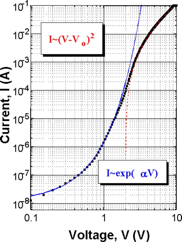
Typical I-V characteristic in a log-log scale. Two regimes of tunneling and space charge limited current are identified at low and high biasing, respectively (see text).

Fedison et al. [22] have reported a similar behavior for low currents in homojunction LEDs as those observed in our devices. However, they can observe a conventional Shockley diffusion current before early saturation of the current occurs. Unfortunately, due to this limitation, the I-V characteristics in our devices cannot provide information on the current mechanisms involved in the junction when the diode is emitting light (voltages higher than 3 V), so that either tunneling, generation-recombination and/or diffusion processes may take place.
4. Electroluminescence spectral response and L-I characteristics
In order to investigate on their electroluminescent properties, the diodes were excited by either a Keithley 220 dc programmable current source, and an HP8116A function generator able to provide voltage pulses with a 50 MHz bandwidth. EL spectra were measured with a high resolution HTR-1000 Jobin Yvon monochromator and a GaAs photomultiplier, using lock-in techniques. White light was also detected by a UV-enhanced Si photodetector.
The evolution of EL spectra under increasing voltage has been studied for dc and ac excitations, both producing a similar behaviour except for the more pronounced thermal effects under dc operation. EL spectra recorded at different ac biasing conditions are shown in Figure 3. At low bias, a broad blue-shifting visible band is observed, while a sharp UV peak (370 nm, FWHM=15 meV) becomes dominant at high voltages. In addition, the typical yellow band (YB) at 560 nm, completely absent at low bias, is enhanced by current injection. The oscillatory pattern seen in the spectra is due to Fabry-Perot interference. The lineshape features an abrupt decrease at high energies due to internal optical absorption. EL spectra have been recorded from the p-side and the n-side of the junction, the latter been more intense because the light is mainly produced below the upper contact. A slight reabsorption of UV light by p-GaN also takes place, since the UV-to-visible ratio is somewhat larger for n-side emission.

EL spectra performed under 1 MHz pulse biasing with several pulse amplitudes.
The visible emission, which appears at 3 V excitation as a broad and weak band centered around 550 nm, increases in intensity and shifts down to 430 nm for high injection (or pulse amplitude). It should be clear that this recombination involves deep centers and not shallow acceptors, since no emission at 390 nm is observed. The transition does not behave as a typical DAP, since it experiences a very large shift, indicating that the defects are located in a broad, multi-level band. The energy shift is due to saturation of the lowest energy levels, either if they behave as deep donors or as deep acceptors. The shifting behaviour of the visible band under increasing bias has also been observed in InGaN [14] [15] [16] and homojunction MOCVD GaN LEDs [4] [11] [14]. In most cases, it is interpreted as due to tunneling transport across the junction through one or several intermediate states.
The broad blue-violet emission has also been observed by low temperature PL in highly Mg-doped GaN layers [7]. This band blue-shifts by around 100 meV for a 2-decade increasing excitation intensity [9] [13], in the same way as observed for the visible emission in EL spectra for increasing current. Whatever the current mechanism involved, the blue recombination process takes place at the p-side of the junction.
EL spectra recorded at different temperatures are shown in Figure 4 for a relatively low current injection (~10 µA at 4K, ~10 mA at RT). The dominant emission at 4K peaks at 388 nm (3.20 eV), being due to recombination between residual donors and the shallow acceptor (DAP). However, this emission is thermally quenched and the band at 430 nm (2.88 eV) involving deep levels is observed at RT. This significant change in the LED operation might be explained by the ionization of the shallow acceptor and compensation by the presence of donors, either residual or diffused Si.

dc EL spectra at several temperatures, under low bias to avoid heating of the device.
The light-current characteristics have been obtained both from a direct measurement of the light (full symbols in Figure 5) and by integration of the EL spectra obtained at several voltages (open circles). In agreement with the spectral evolution, the L-I curve shows a superlinear dependence at low current (L ~ Im, with m=2.3), which becomes almost linear (m=0.9) when the defects are saturated. This behaviour has also been observed in Nichia LEDs [23]. The change in slope corresponds to the bias for which the blue emission is stacked at 430 nm, and its intensity is also saturated. The relative efficiency, dL/dI vs I, is shown in the inset to Figure 5. A slight decrease is observed for I>50 mA, which likely corresponds to some heating of the LED as also deduced from the small red-shift of the UV band at increasing currents.

L-I log-log characteristics. Inset: Relative efficiency characteristics, dL/dI vs I. Full and open symbols represent the light measured by a Si photodetector and the integrated EL spectra like those shown in Figure 3, respectively. Solid curves are linear fits in the low and high current injection regimes.
5. Electroluminescence time response
A more careful study of the EL spectra is needed in order to elucidate the nature of the deep levels. Some EL experiments have been performed under different conditions of pulsed excitation, by changing the pulse duration t ON or the duty cycle δ at fixed pulse amplitude.
Figure 6 shows EL spectra recorded under pulsed excitation, with 7 V pulses of increasing duration. Each spectrum has been renormalized to give the average spectral intensity during the time while the pulse is in the ON state. It is assumed that the device was switched off for enough time before the pulse is active (long tOFF). The small red-shift from 370 to 375 nm observed for increasing tON is likely due to heating of the device when it is emitting for a long time. As observed in Figure 6, the UV emission is constant with time, indicating the continuous supply of both electrons and holes. On the contrary, the blue emission at 430 nm shows a clear decay, which is attributed to an inhibition of this recombination path due to a long relaxation time of the acceptor. The EL intensity of this band is plotted in Figure 7 vs the pulse duration, from which the exponential fit

EL spectra recorded at 7V amplitude pulses of different duration.

Time evolution of the violet EL intensity.
provides the saturation time of the acceptor level τsat ≈ 135 ns.
In order to obtain direct information on the relaxation time of the acceptor τ10, the diode has been excited by pulses of fixed duration and variable frequency f or duty cycle δ = f·tON = tON / (tON + tOFF). EL spectra obtained under 7 V, 200 ns pulses for frequencies between 200 kHz and 4 MHz (duty cycles δ from 0.04 to 0.8, respectively), are shown in Figure 8. The measured intensity has been corrected to give the average light emitted in each pulse. The UV radiation does not depend on δ (i.e. on the rest time tOFF), whereas the visible intensity clearly decreases with δ . In other words, a long time is needed so that the involved acceptors are recharged with holes. This relaxation time is obtained by fitting the intensity vs t (= tOFF) to the expression

EL spectra recorded at 7V amplitude, 200 ns pulses, at several frequencies (duty cycles).
as illustrated in Figure 9, with the result τ10 ≈ 1.06 µs.

Violet EL intensity observed after different rest time tOFF.
6. Discussion
The deep levels which dominate the EL response (broad and red-shifting violet-blue band) are due to the presence of Mg-related defects, which form a continuum of states, as suggested above, whereas the UV emission is grossly due to band-to-band recombination. The UV-to-blue ratio increases with pulse amplitude, as shown in Figure 3, pointing to the saturation of the deep defects involved in the visible emission. Additionally, for a fixed amplitude, the longer the pulse the higher UV/visible ratio, as observed in Figure 6. In other words, the injected carriers are trapped first by the states which generate the blue band, as also reported for the Nichia DH-LED by Basrur et al [17]. Besides, the UV-to-visible emission ratio at constant pulse duration is optimized by using high duty cycles (Figure 8), in order to block the visible band emission. All this requirements for the amplitude, duration and duty cycle of the pulsed biasing in order to improve the UV emission contribute to heat the device.
Basrur et al. describe the visible and UV generation mechanism by a four-level system, which implies that visible emission involves transitions from donors to acceptors in the depletion layer. Lifetimes of 5 and 115 ns for the UV and blue bands are obtained, with a relaxation time for the acceptor as low as 0.8 ns (more than one thousand times smaller than in our device). Therefore, the visible emission in these candela-class DH-LEDs involves shallower levels instead than the deep centers introduced by Mg-doping.
6.1. Nature of deep levels
Figure 10 shows a model with all the levels which could potentially be involved in the radiative recombinations of our GaN LEDs. The blue-violet emission is likely to take place at the p-side of the junction. Deep centers involved in the blue-violet emission could behave either as donors or as acceptors. The first attribution has been recently proposed to justify the two-peak shape of PL spectra at 2.7 and 2.9 eV [9] [13]. The incorporation of deep donors as a result of heavy Mg doping would also explain why it is so difficult to obtain p-type material. However, a transition between deep donors (labelled DLD in Figure 10) and the shallow acceptor (SA) level or the valence band (VB) cannot explain our observations, because it would be characterized by a very fast relaxation.

Level recombination model of the GaN UV-blue LED. RD and Si stand for shallow donors, SA for shallow acceptors, DLD and DLA for deep levels behaving as donors and acceptors, respectively, and YBA for the deep acceptors involved in the yellow luminescence. The UV and visible emissions at the p-side region are explained by a simple 3-level system involving levels 2, 1 and 0.
An alternative possibility is to consider the deep level as an acceptor. This interpretation would not be appropiate if only tunneling currents are taken into account. However, other current mechanisms could contribute to the EL as previously indicated. Actually, the visible emission could be produced by the recombination of electrons from the conduction band (CB) or shallow residual donors (RD) to a deep acceptor related to Mg in the p-type layer (DLA). In this way, both requirements of a continuous supply of electrons and a long relaxation time of the acceptor are satisfied.
Together with deep acceptors, deep donors may also be present in the heavily doped p-type layer. However, only two clearly resolved bands in the UV and visible regions are seen. In addition, the time behaviour observed for the blue EL intensity suggests t hat the recombination path through deep donors is less probable than that through deep acceptors. Therefore, the contribution to EL from deep donors to acceptors or valence band will be neglected.
6.2. Levels model
In practice, a simple 3-level system is enough to justify the EL at the p-side of the p-n junction, as illustrated in Figure 10, where level 2 is either the conduction band or the shallow donor, level 1 is the band of deep states, and level 0 is the valence band. The shallow acceptor SA level plays no role in this model, since no EL at 390 nm is seen in the spectra at RT.
A simulation of the level populations N2(t) and N1(t) provides the time dependency for the UV and visible emissions taking place in the p-type region, according to
where J(t) is the current density, d=150 Å, and N is the deep acceptor concentration. A fast UV recombination τ20 = 5 ns has been assumed, and τ20 << τ non2 (non-radiative time of level N2). The lifetime τ21 depends on N1, while τ10 = 1.06 µs and the empty band recombination time, τ′21, are constant. Using τsat=135 ns to fit the visible intensity decay, τ′21≈70 ns is obtained. The time evolution of the UV and visible emissions are in full agreement with the observations: LUV(t)~N2(t) shows a very slight increase while LVIS(t)~N2(t)/ τ21(t) decreases with time in the same fashion as observed for the blue-violet EL intensity.
6.3. Origin of deep levels
Deep acceptor states lie around Eg-EVIS ≈ 0.55 eV above the valence band (actually, this is the lower energy of the broad band of levels in the gap). This energy is compared with results from first-principles calculations in order to identify the origin of the deep acceptors, which should involve defects associated with Mg doping. Here, both acceptors and ionized donors should be taken into account as possible defects involved in the blue emission. Deep donors associated to nitrogen vacancies in p-type material (VN3+, at 0.9 eV above the valence band [25]), related to Mg doping (VN-Mg2+, at 0.7 eV above the valence band [25]), and also hydrogenated nitrogen vacancies (VN-H [26]) could be involved in the blue-violet emission.
On the other hand, the UV emission at 370 nm (3.35 eV) should be due to one (or both) of the following processes:
-
1)
generation-recombination in the n-side of the junction, from Si donors to valence band
-
2)
radiative recombination at the p-side, involving residual donors fed by diffusion of electrons.
The yellow emission, from shallow donors to an acceptor (YBA in Figure 10), is likely to occur in the n-type region, as suggested by the fact that it is not observed in the PL spectra of heavily doped GaN [7]. Deep acceptors in n-type GaN have been attributed to VGa-H complexes [27]. Either trapping of diffused holes by the YBA, or tunneling from the deep acceptor in the p-type side could take place. Some contribution to the YB could also be due to a PL emission after reabsorption of the UV electroluminescence in the bulk.
7. Conclusions
A detailed characterization of the electrical and optical properties of MOVPE GaN p-n homojunction light emitting diodes has been performed. The EL spectra consist of a blue-violet emission (430 nm) involving acceptor deep states generated by Mg doping located 0.55 eV above the valence band, a UV band-to-band recombination at 370 nm, and the YB. The blue and YB emissions take place at the p-side and n-side of the p-n junction respectively, whereas the UV recombination may be produced at both regions. The p-type emissions can be explained by a simple 3-level model, with intrinsic recombination times τ′21 ≈ 70 ns and τ10 ≈ 1.0 µs. The UV-to-visible emission ratio is optimized by using intense and long pulses, at high duty cycles, in compromise with heating of the device. The UV emission is therefore much more efficient and monochromatic than the blue-violet emission. In order to optimize the LED performance, a better activation of the p-dopant species or a new dopant (like Zn) are needed. Furthermore, the optimum blueLED should be achieved by using an InGaN active layer with the proper In content which gap energy matches the required wavelength emission.
References
S. N. Mohammad, A. A. Salvador, H. Morkoç, Proc. IEEE 83, 1306–1355 (1995).
Shuji Nakamura, Gerhard Fasol, The Blue Laser Diode - GaN based Light Emitters and Lasers (Springer-Verlag, Heidelberg, 1997).
H. Amano, M. Kito, K. Hiramatsu, I. Akasaki, Jpn. J. Appl. Phys. 28, L2112 (1989).
S. Nakamura, T. Mukai, M. Senoh, N. Iwasa, Jpn. J. Appl. Phys. 31, L139–L142 (1992).
W. Gotz, N. M. Johnson, J. Walker, D. P. Bour, R. A. Street, Appl. Phys. Lett. 68, 667–669 (1996).
P. Hacke, H. Nakayama, T. Detchprohm, K. Hiramatsu, N. Sawaki, Appl. Phys. Lett. 68, 1362–1364 (1996).
F. J. Sanchez, F. Calle, D. Basak, J. M. G. Tijero, M. A. Sánchez-García, E. Monroy, E. Calleja, E. Muñoz, B. Beaumont, Pierre Gibart, J.J. Serrano, J.M. Blanco, MRS Internet J. Nitride Semicond. Res. 2, 28 (1997).
M. Smith, G. D. Chen, J. Y. Lin, H. X. Jiang, A. Salvador, B. N. Sverdlov, A. Botchkarev, H. Morkoc, B. Goldenberg, Appl. Phys. Lett. 68, 1883–1885 (1996).
S. Haffouz, B. Beaumont, M. Leroux, M. Laugt, P. Lorenzini, Pierre Gibart, L.G. Hubert-Pfalzgraf, MRS Internet J. Nitride Semicond. Res. 2, 37 (1997).
S. Nakamura, T. Mukai, M. Senoh, Jpn. J. Appl. Phys. 30, L1998 (1991).
B. Golenberg, J. D. Zook, R. J. Ulmer, Appl. Phys. Lett. 62, 381 (1993).
M. Schauler, C. Kirchner, M. Mayer, A. Pelzmann, F. Eberhard, Markus Kamp, P. Unger, K. J. Ebeling, MRS Internet J. Nitride Semicond. Res. 2, 44 (1997).
B. Beaumont, S. Haffouz, P. Gibart, M. Leroux, Ph. Lorenzini, E. Calleja, E. Muñoz, unpublished (1998).
H. C. Casey, J. Muth, S. Krishnankutty, J. M. Zavada, Appl. Phys. Lett. 68, 2867 (1996).
P Perlin, M Osinski, PG Eliseev, VA Smagley, J Mu, M Banas, P Sartori, Appl. Phys. Lett. 69, 1680–1682 (1996).
PG Eliseev, P Perlin, J Furioli, P Sartori, J Mu, M Osinski, J. Electron. Mater. 26, 311–319 (1997).
J. P. Basrur, F. S. Choa, P. -L. Liu, J. Sipior, G. Rao, G. M. Carter, Y. J. Chen, Appl. Phys. Lett. 71, 1385 (1997).
Shuji Nakamura, Takashi Mukai, Masayuki Senoh, Appl. Phys. Lett. 64, 1687–1689 (1994).
R. P. Vaudo, I. D. Goepfert, T. D. Moustakas, D. M. Beyea, T. J. Frey, K. Meehan, Appl. Phys. Lett. 79, 2779 (1996).
N. Grandjean, J. Massies, M. Leroux, P. Lorenzini, Appl. Phys. Lett. 72, 82 (1998).
B. Beaumont, M. Vaille, T. Boufaden, B. el Jani, P. Gibart, J. Cryst. Growth 170, 316–320 (1997).
J. B. Fedison, T. P. Chow, H. Lu, I. B. Bhat, Appl. Phys. Lett. 72, 2841 (1998).
I Martil, E Redondo, A Ojeda, J. Appl. Phys. 81, 2442–2444 (1997).
J. A. Edmond, K. Das, R. F. Davis, J. Appl. Phys. 63, 922 (1988).
CH Park, DJ Chadi, Phys. Rev. B 55, 12995 (1997).
C. G. Van de Walle, Phys. Rev. B 56, R10023 (1997).
J Neugebauer, CG Van de Walle, Appl. Phys. Lett. 69, 503–505 (1996).
Acknowledgments
The authors would like to acknowledge Drs. J. Neugebauer, I. Izpura, and I. Mártil for interesting and useful discussions. This work is supported by CICYT TIC95-0770 and ESPRIT LAQUANI 20968 Projects.
Author information
Authors and Affiliations
Rights and permissions
About this article
Cite this article
Calle, F., Monroy, E., Sánchez, F.J. et al. Analysis of the Visible and UV Electroluminescence in Homojunction GaN LED’s. MRS Internet Journal of Nitride Semiconductor Research 3, 24 (1998). https://doi.org/10.1557/S109257830000096X
Received:
Accepted:
Published:
DOI: https://doi.org/10.1557/S109257830000096X