Abstract
Silicon carbide (SiC) has emerged as a significant wide bandgap semiconducting material, playing a pivotal role in the fabrication of high-frequency, high-power electronic devices in modern times. Its exceptional properties, such as high thermal conductivity, high saturation velocity, and high breakdown field, have positioned it as a valuable constituent in various application fields, including transportation, communication, and bioelectronics. However, the efficacy and long-term reliability of SiC-based devices are critically dependent on the quality of both the SiC substrate and epitaxial material employed. The presence of deleterious defects within these materials can induce device degradation and failure, posing a significant challenge in realizing the full potential of the device. Therefore, it is imperative to address the quality while maintaining the availability of large-scale single crystals of SiC to further expand the development of SiC-based device technology. Among various kinds of crystallographic defects in bulk crystal, low angle grain boundary (LAGB) is a commonly observed planar defect that prevents the implementation of large size (≥ 1 cm2) SiC devices [1]. In both 6H and 4H-SiC, LAGBs have been observed to replicate during the epitaxial growth [2], which can lead to profound impact on the physical and electronic properties of the crystal that subsequently triggers device degradation. Literature reveals that the presence of LAGBs in commercial wafers can lead to increased leakage currents during reverse-bias operation of devices [3]. Besides, the existence of prismatic tilt boundaries is usually accompanied with aggregation of edge type basal plane dislocations (BPDs) [4], which cause severe degradation in SiC bipolar devices [5] as BPD segments can dissociate into partials and form stacking faults in between [6].
This study investigated a unique distribution pattern of LAGBs observed on physical vapor transport (PVT) grown off-axis 4H-SiC wafers. Synchrotron X-ray topographs in both transmission and grazing geometry reveal that three sets of LAGBs are presented on one side of the wafer, away from the facet position, each set contains numerous LAGB arrays. Figure 1 (a) shows a schematic diagram where each oval outlines the approximate location of each LAGB set. As the grazing-incidence topographs shown in Figure 1 (b), the LAGB sets distributed at the upper and lower region of the wafer consist of white contrast threading edge dislocations (TEDs) extending from the inner area towards the edge approximately along 60º and 120º direction, respectively. The LAGB set positioned at the middle region of the wafer consists of dark contrast TEDs extending from the inner area towards the edge approximately along 90º direction. All individual TED arrays in each LAGB set extends along the <1-100> directions, with identical Burgers vectors perpendicular to the array direction. The white and dark contrast of TEDs corresponds to tilt in opposite directions. White contrast TEDs are with Burgers vectors of 1/3[2-1-10] and 1/3[1-210], dark contrast TEDs are with Burgers vectors of 1/3[-2110] and 1/3[-12-10]. Such TED LAGBs are identified as pure tilt boundaries that accommodate the rotational misorientation between two adjacent regions. Therefore, a flat wafer is expected to exhibit zero net misorientation due to these TED arrays. However, any non-zero net misorientation resulting from these arrays is likely to promote instability, ultimately leading to the curvature of the plane. A systematic analysis is being carried out across several wafers and this relationship between the distribution of TED arrays and lattice curvature will be discussed.
Reference:
[1] N. Ohtani et al. Journal of Crystal Growth237–239, 1180–1186, (2002).
[2] C. Hallin et al, J. Cryst. Growth181, 241 (1997).
[3] R. Singh and M. Pecht, IEEE Industrial Electronics Magazine, 2, 19-31, (2008).
[4] Y Chen et al, Materials Science Forum556, 231-234 (2007).
[5] T. Kimoto, et al., Proc. IEEE Int. Rel. Phys. Symp., 2A-1.1–2A-1.7, (2017).
[6] M. Dudley, et al, Materials Science Forum, 600-603, 261-266 (2008).
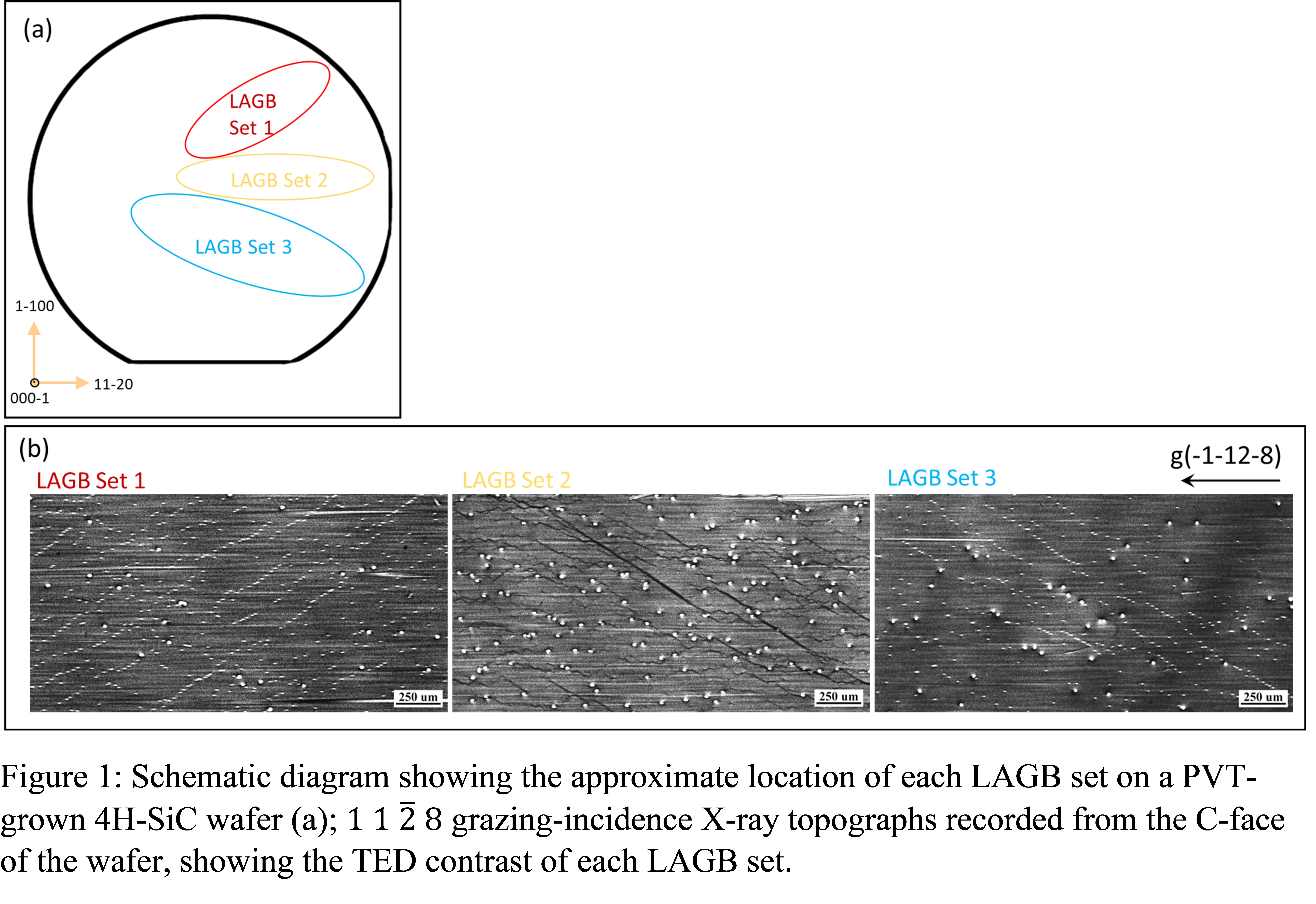
Figure 1