Abstract
Two-dimensional (2D) materials have attracted much attention over the last decade due to their high performance in nanoelectronic devices. The discovery of graphene opened up many opportunities to investigate and explore other 2D materials. There has been a drive to expand the toolbox of 2D materials to also include insulators and semiconductors with a variety of bandgaps. As a result, a wide range of materials have been discovered or predicted,1 with molybdenum disulfide (MoS2) being particularly popular. The semiconducting phase of MoS2 (2H-MoS2) is one of the most commonly studied among the transition metal dichalcogenides.2 It has a thickness dependent band gap which has drawn attention for field-effect transistors (FET) where a high on/off current ratio is desired.3-5 However, for applications in batteries,6supercapacitors,7 and solar cells,8 a substantially increased conductivity is required in order to achieve reasonable currents. Using 2H-MoS2 requires a relatively high voltage to get sufficient conductivity due to the presence of a band gap. The most common source of conductive MoS2 is metallic MoS2 (1T-MoS2) that has been prepared via the lithium intercalation process, which requires inert atmosphere processing and safety procedures.9 Hence, there is a desire to develop a safer and more efficient process to yield conductive MoS2.
Defects plays a very important role in modulating the electrical properties of MoS2. Sonication of MoS2 in an appropriate solvent results in many disordered structural defects. The most common defects on MoS2 are sulfur defects.10 These defects increase the energy level of the gap state and eventually deteriorate the device performance. Thiol based molecules are commonly used to reduce the number of sulfur defects on MoS2.11 Other molecules such as oxygen or organic super acids like bis(trifluoromethane) sulfonamide (TFSI) have also been reported to passivate the surface defect.12,13 Past research has mainly focused on the theoretical study of defective MoS2 and how to utilize those defects for improving photoluminescent efficiency. However, those defects can also be utilized to improve the conductivity of MoS2 as a safer alternative for applications in batteries, supercapacitors, solar cells and sensors.
In this work, we show a simple and effective way to prepare few layer conductive MoS2 under ambient conditions. We have demonstrated that the sheet resistance of the conductive MoS2 that we prepared is up to five orders of magnitude higher than that of the semiconducting phase of MoS2, depending on the dopant concentration. The samples were also characterized with Hall measurements, X-ray photoelectron spectroscopy (XPS) and Raman spectroscopy. An important goal of our work is to control the conductivity of the MoS2 thin films in safe and facile ways that enable their application in low-cost chemiresistive sensors in liquid environments. We fabricated chemiresistive pH sensors with centimeter channel lengths while maintaining low measurement voltages. Our study furthers the understanding of conductive forms of MoS2, and also opens a new pathway for next generation electronic devices.
References:
1. M. D. Segall et al., J. Phys.: Condens. Matter, 14, 2717–2744 (2002).
2. H. Wan et al., RSC Adv., 5, 7944 (2015).
3. D. Kiriya et al., J. Am. Chem. Soc., 136, 7853−7856 (2014).
4. H. Fang et al., Nano Lett., 13, 1991−1995 (2013).
5. M. Choi et al., ACS Nano, 8, 9332-9340 (2014).
6. T. Stephenson et al., Energy Environ. Sci., 7, 209-231 (2014).
7. L. Cao et al., Small, 9, 2905–2910 (2013).
8. M.-L.Tsai et al., ACS Nano, 8, 8317-8322 (2014).
9. G. Eda et al., Nano Lett., 11, 5111–5116 (2011).
10. A. Dabral et al., Phys. Chem. Chem. Phys., 21, 1089-1099 (2019).
11. D. M. Sim et al., ACS Nano, 9, 12115-12123 (2015).
12. K. C. Santosh et al., J. Appl. Phys., 117, 135301 (2015).
13. H. Lu et al., APL Mater., 6, 066104 (2018).
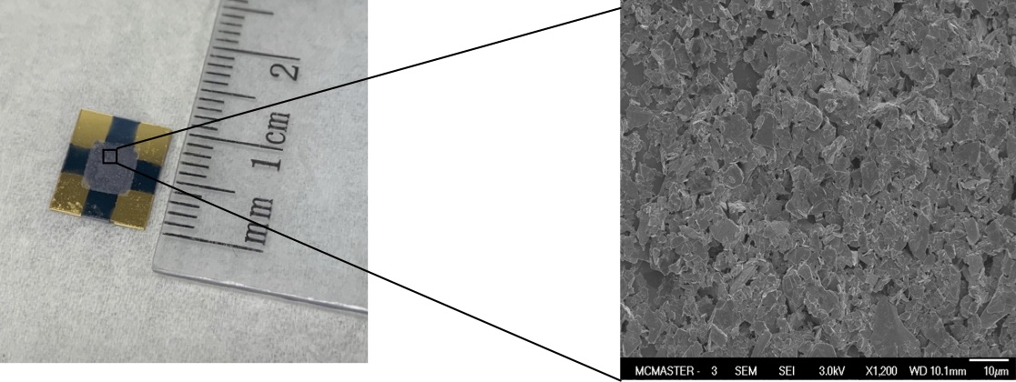
Figure 1