

Abstract
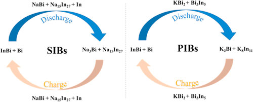
Sodium ion batteries (SIBs) and potassium ion batteries (PIBs) are promising post-lithium candidates for grid-scale energy storage, and understanding of the Na/K chemistry is crucial for the development of advanced electrode materials. Herein, a nanoporous indium-bismuth (np-InBi) alloy was fabricated by chemical dealloying of a ternary Mg-In-Bi precursor, and shows a three-dimensional ligament-channel structure. As the anode for SIBs and PIBs, the np-InBi alloy exhibits decent initial discharge capacity. More importantly, the Na/K storage mechanisms of the np-InBi electrode were investigated using operando X-ray diffraction (XRD). The operando XRD results demonstrate that the (de)sodiated mechanism of the np-InBi electrode in SIBs involves (de)alloying processes between InBi + Bi to Na3Bi + Na15In27 via the intermediate products of NaBi + Na15In27 + In. Simultaneously, the (de)potassiated mechanism of the np-InBi electrode in PIBs yields the reversible processes of InBi + Bi ↔ KBi2 + Bi3In5 ↔ K3Bi + K8In11.
Export citation and abstract BibTeX RIS

This is an open access article distributed under the terms of the Creative Commons Attribution 4.0 License (CC BY, http://creativecommons.org/licenses/by/4.0/), which permits unrestricted reuse of the work in any medium, provided the original work is properly cited.
Post-lithium batteries including sodium ion batteries (SIBs) and potassium ion batteries (PIBs) have aroused extensive attention as promising alternatives to lithium ion batteries (LIBs) especially for grid-scale energy storage owing to the natural abundance, easy access and low cost of Na and K. 1–4 In general, the successful design strategy of LIBs can be analogously applied and thus efficiently accelerate the exploration for advanced electrodes in SIBs and PIBs. However, the large ionic radius of Na/K (1.02/1.38 Å for Na+/K+ vs 0.76 Å for Li+) leads to sluggish electrochemical kinetics and dramatic volume expansion, significantly reducing the rate capability and lifespan of the electrode. 5,6 Therefore, there is an urgent need to nanoengineer the electrode materials with proper porous architecture to alleviate the volume expansion/contraction & eliminate the resistance, and deeply understand the (de)alloying mechanism during cycling via operando (in situ) spectroscopy methods (such as operando X-ray diffraction (XRD), Raman technique, transmission electron microscopy (TEM), on-line differential electrochemical mass spectrometry (DEMS), and so on) to find the key limitation and guide the subsequent electrode design. 7,8
Alloy anodes including Bi, In, Sb, Sn, etc., are promising as potential candidates for SIBs and PIBs due to their extraordinary Na+/K+-storage capacities and proper working potentials, but are limited by the electrochemically-induced unstable surface electrolyte interphase (SEI) films and pulverization/aggregation related with the tremendous volumetric variations. 9–12 Among all sorts of alloys used, the InBi alloy would be an ideal choice due to the following reasons. (I) In has considerable deformability, which can effectively withstand severe volume change during cycling. 13 (II) In and Bi possess moderate theoretical gravimetric capacity of 467 mAh g−1(Na2In) and 385 mAh g−1(Na3Bi) in SIBs, respectively. 14 (III) InBi exhibits the layer-like crystal structure with the relative weak interlayer binding, which may be beneficial for the ion transfer. 15 (IV) In and Bi can serve as mutual buffer substrates to accommodate volumetric variations because of different (de)sodiated/(de)potassiated potentials. For example, Murgia et al. have reported the moderate lifespan under the sluggish magnesiated kinetics and complex reaction pathway of InBi anode, not only implying the promising capability in storing the large Na+/K+ ions, but also emphasizing the significance for clarifying the interaction between In and Bi. 16 Simultaneously, the sodiated/potassiated processes of In are varied in different In-based compounds in terms of previous reports, exhibiting partial irreversibility (In-Sb-S 11 ), complete inert (In-S 17,18 ) as well as complete reversibility (In-Sb 19 /Zn-In-S 20 /In2Se3-CoIn2-CoSe2 21 ), which attaches more importance for deeply comprehending the relationship between the sodiation/potassiation behaviors of In and the composition of In-based compounds. However, to our best knowledge, the InBi anode has not be applied in SIBs/PIBs and the corresponding (de)sodiated/(de)potassiated mechanisms of InBi are still unknown. Notably, chemical dealloying is an efficient method to fabricate the nanoporous architecture, where the most electrochemically active element(s) in the alloy precursors can be selectively etched, leaving the (nano)porous ligament-channel structure. 22 Such method has been extensively utilized in the battery field owing to the unique mechanical, physical and chemical properties of the dealloying-induced architecture. 23
Herein, nanoporous InBi (np-InBi) alloy was designed and fabricated by chemical dealloying of an Mg-In-Bi precursor. As an anode for SIBs/PIBs, the np-InBi alloy shows good electrochemical storage capacity for both Na+ and K+ ions. More importantly, operando XRD technique was utilized to real-timely investigate the Na+/K+-storage mechanisms (crystalline products) of the np-InBi anode. In SIBs, the np-InBi electrode follows (de)alloying processes between InBi + Bi to Na3Bi + Na15In27 via the intermediate products of NaBi + Na15In27 + In. Moreover, the np-InBi anode in PIBs yields the reversible processes of InBi + Bi ↔ KBi2 + Bi3In5 ↔ K3Bi + K8In11.
Experimental
Material preparation
The np-InBi alloy was synthesized by chemical dealloying of a ternary Mg92In4Bi4 (nominal composition, at%) precursor. Firstly, under the protection of the Ar gas, pure Mg, In and Bi blocks (purity, 99.9 wt%) were melted in a graphite crucible using a vacuum induction melting furnace, and then cast into a mold to form the Mg92In4Bi4 ingot. Secondly, the ingot was further rapidly solidified into foils with the thickness of tens of microns by utilizing a melt-spinning apparatus (at a speed of 1500 revolutions per minute (rpm)) under the Ar atmosphere. Thirdly, the Mg92In4Bi4 foils were dealloyed in a 2 wt% tartaric acid solution at room temperature until no bubbles appeared. Finally, the dealloyed samples were thoroughly rinsed with deionized water and ethanol, followed by drying in vacuum at 60 °C for 10 h. For the fabrication of the p-In, the experimental procedures were analogous except that the precursor was Mg92In8 (at%).
Microstructural characterizations
The phase constitutions of the as-prepared samples were identified utilizing an XD-3 diffractometer (Beijing Purkinje General Instrument Co., Ltd., China) equipped with Cu Kα radiation. The microstructure of the samples was characterized by scanning electron microscopy (SEM, JSM-7610F) and transmission electron microscopy (TEM, JEOL-JEM-2100). The measurement for the scale of ligaments was conducted by Software Nano Measurer (Version: 1.2.5). An energy dispersive X-ray (EDX) analyzer coupled with SEM (COXEM EM-30) was used to determine chemical compositions of the samples.
Electrochemical measurements
All electrodes were prepared by a scrapping-coating method. The slurry was fabricated by mixing the active material powders, conductive agent (Super P), and carboxymethyl cellulose (CMC) binder in terms of a weight ratio of 7: 2: 1 in deionized water, followed by stirring for approximately 12 h to form a homogeneous slurry and subsequently coated onto a stainless steel mesh (type 304, thickness: 0.1 mm) for operando XRD, or Cu foil for other electrochemical measurements. The electrodes were further dried at 80 °C for 12 h in vacuum, and then the disks (diameter: 12 mm) were punched with the mass loading of ∼1.0 mg cm−2. Na/K foil (purity: 99.8 wt%, Sigma-Aldrich) was adopted as both the counter and reference electrodes, while the glass fiber (GF/D, Whatman) was used as the separator. The electrolyte was 1 M NaClO4 in propylene carbonate (PC) with 5 wt% addition of fluoroethylene carbonate (FEC) (ester-based) or 1 M NaPF6 in diglyme (ether-based) for SIBs, and 1 M KFSI in ethylene carbonate (EC)/diethyl carbonate (DEC) solvent mixture with 1:1 by volume (ester-based) or 3 M KFSI in 1,2-dimethoxyethane (DME) (ether-based) for PIBs. The CR2032 cells were assembled in an argon-filled glove box and then aged for 24 h before tests. For the operando XRD, a home-made CR2032 coin cell was used equipped with one side Be window (10 mm in diameter) transparent for X-ray. The electrolytes used for operando XRD were ester-based electrolytes (1 M NaClO4 in PC with 5 wt% FEC for SIBs, and 1 M KFSI in EC/DEC solvent mixture with 1:1 by volume for PIBs). The ester-based electrolyte is more stable compared with the ether-based electrolyte, and suitable for the operando research. Meanwhile, the solvent type mainly determines the properties of the SEI film to influence the electrochemical performance, and is not significantly related with the reaction mechanism during cycling. 24 The XRD patterns were collected based on a "time step" method through the window of the coin cell, cycled at low current densities. In the "time step" mode, the scan rate of XRD was determined by the count time (herein, 8 s) for each degree point, to enhance the intensity of the XRD pattern with enough count time. Galvanostatic measurements and galvanostatic intermittent titration technique (GITT) were evaluated by the test system (LAND-CT2001A, Wuhan, China). Cyclic voltammograms (CVs) were obtained by a CHI 660E potentiostat. Electrochemical impedance spectroscopy (EIS) measurements were carried out by a Zahner Zennium potentiostat at open circuit voltage (OCV) and the charged state. The frequency range was set from 10 mHz to 100 kHz with an excitation voltage of 5 mV.
Results and Discussion
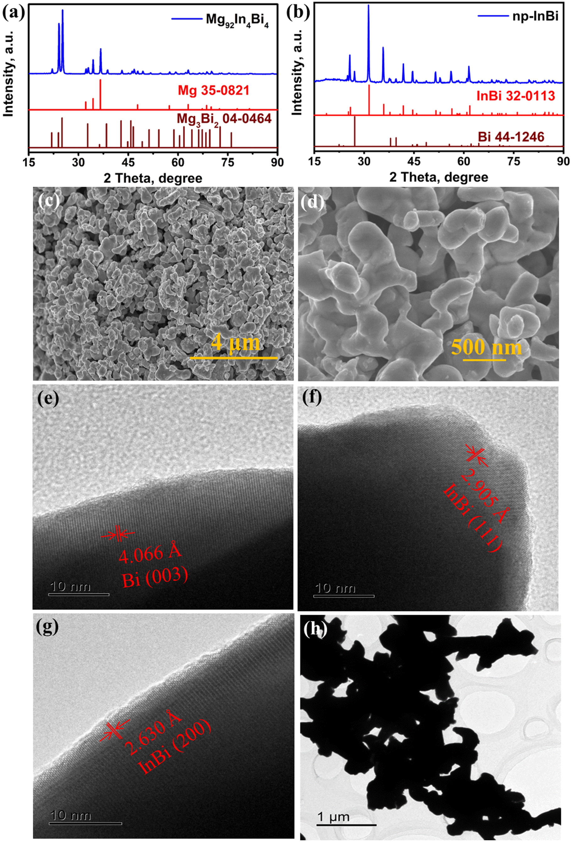
The XRD pattern of the Mg92In4Bi4 foils (Fig. 1a) is indexed to Mg3Bi2 (JCPDS # 04–0464) and Mg (JCPDS # 35–0821) phases where In solubilizes due to its high solid solubility in Mg as depicted by the phase diagram of the Mg-In system (Fig. S1). 25 The high content (92 at%) of Mg was chosen for not only exceeding the "parting limit" to avoid the compositional and geometric restrictions on dealloying, 26,27 but also increasing porosity of the dealloyed samples for facilitating the ion transportation and mitigating the volumetric change. Additionally, the precursor composition was chosen to be close to the eutectic point of the Mg-Bi system according to the Mg-Bi phase diagram, in order to refine the size of the eutectic microstructure (Mg(In)/Mg3Bi2). After dealloying, the predominant peaks of Mg3Bi2 and Mg(In) phases of the Mg92In4Bi4 foils disappeared, and the XRD pattern of the np-InBi alloy could be assigned to InBi (JCPDS # 32–0113) and Bi (JCPDS # 44–1246) phases (Fig. 1b). Here, the peaks belonging to Bi are much weaker in comparison with those of InBi. The Rietveld refinement for the XRD pattern of np-InBi was conducted to calculate the phase constitution of np-InBi (Fig. 1b and Fig. S2), showing that the mass fractions of the InBi and Bi phases are 94.7 and 5.3 wt% respectively and thus confirming the small amount of Bi in the np-InBi alloy. The SEM images (Figs. 1c–1d) elucidate that the np-InBi samples show a three-dimensional ligament-channel structure where the mean size of ligaments is 279.0 ± 70.8 nm (Fig. S3). Additionally, the EDX results (Fig. S4) reflect that the actual atomic ratio of the np-InBi alloy is close to its nominal composition. Only a minor amount of Mg is detected, and both the In and Bi elements are homogeneously distributed in the np-InBi alloy. TEM was utilized to further characterize the microstructure of the np-InBi alloy (Figs. 1e–1h). The high-resolution TEM (HRTEM) images (Figs. 1e–1g) reveal that the lattice fringes can be well distinguished, matching with the crystal planes of Bi (003), InBi (111) and (200), further confirming the presence of Bi and InBi in the np-InBi alloy. As depicted in Fig. 1h, the nanoporous feature can be clearly observed with the ligament size of 303.1 ± 109.4 nm (Fig. S3), which is consistent with the SEM results. Herein, the formation of such structure can be attributed to the dealloying procedure. During the dealloying process in the tartaric acid solution, the active element (Mg) in the Mg(In) and Mg3Bi2 phases of the Mg-In-Bi precursor was selectively etched away, while the inert elements (In and Bi) were retained and reorganized via surface diffusion to form the nano-sized ligament-channel structure. 22

Figure 1. (a), (b) XRD patterns of (a) the rapidly solidified Mg92In4Bi4 foils and (b) the as-dealloyed np-InBi powders. (c)–(d) SEM images of the np-InBi alloy. (e)–(g) HRTEM and (h) TEM images of the np-InBi alloy.
Download figure:
Standard image High-resolution imageTo evaluate the electrochemical performance of the np-InBi electrode for SIBs, CVs and galvanostatic (dis)charge measurements were performed in the ester-based electrolyte. Figure 2a shows the CVs profiles of the np-InBi electrode during the initial cycles at the scan rate of 0.1 mV s−1. In the first cathodic scan, the peaks at 0.22/0.36/0.52/0.85 V (vs Na+/Na) can be attributed to the SEI formation and sodiation of np-InBi, followed by the peaks at 0.09/0.52/0.62/0.73/0.79 V (vs Na+/Na) in the anodic scan which are associated with the desodiation of np-InBi. In subsequent cycles, a slight shift of cathodic peaks can be observed accompanied with the well overlapping of the anodic peaks. Figure 2b shows the discharge-charge curves of the np-InBi electrode during the initial cycles at 0.2 A g−1, which delivers the initial discharge capacity of 474.6 mAh g−1 with the initial Coulombic efficiency (ICE) of 89.8% (Fig. S5). Notably, such high ICE is important for the potential industrial application accompanied with the strict electrolyte amount control. 28 However, the cycling stability of the np-InBi electrode is unsatisfactory, and the specific capacity rapidly decays within 15 cycles. The poor cycling stability stems from the pulverization/aggregation and unstable SEI film formation induced by dramatic volumetric variation and ester-based electrolyte. 29

Figure 2. Electrochemical measurements for the np-InBi anode in SIBs. (a) CVs at the scan rate of 0.1 mV s−1 and (b) discharge-charge curves for different cycles at 0.2 A g−1. (c) Nyquist plots and (d) corresponding relationship in the low frequency range between Z' and ω−1/2 at OCV and the charged state after the 1st cycle. (e) The GITT profiles during the 1st cycle. (f) The diffusion coefficients for Na+ ions as a function of voltage calculated from the GITT profiles in (e).
Download figure:
Standard image High-resolution imageThe ion/electron transfer properties were further probed with EIS and GITT. Figure 2c shows the Nyquist plot of the np-InBi electrode at OCV and the charged state after the 1st cycle, which are further analyzed by fitting equivalent circuits (Fig. S6). The Warburg factor (Fig. 2d) was obtained from the relationship between Z' and ω−1/2 in the low frequency range and utilized to roughly calculate the diffusion coefficient of Na+ (DNa-eis ) in terms of the following equation, 30,31


where R, T, A, n, F, CNa , ω, and σ represent the gas constant, absolute temperature, electrode surface area, number of electrons per molecule, Faraday constant, Na+ concentration in the electrolyte (herein, 1 M) utilized to simplify the gradient concentration of Na+ which is suitable under the relative high frequency area, 30 angular frequency, and Warburg factor. From the calculated results (Table SI), the charge transfer resistance (Rct ) becomes smaller and DNa-eis increases after the 1st cycle, indicating the reduction of impedance and the improved ion diffusion/electron transfer induced by the electrochemical effects. As shown in Figs. 2e–2f, GITT was performed for the np-InBi electrode by intermittently repeated short pulses (current density, 0.05 A g−1) for 1800 s, followed by an open circuit for 7200 s to obtain the equilibrium potential during cycling. The DNa-gitt values at different potentials were estimated according to the Fick's second law of diffusion and following simplified equation, 32–34

where τ is the pulse duration (1800 s), nm is the number of moles, Vm is the molar volume of the alloy obtained from the Materials Project Database (fixed without considering the volume variation), 35 A is the electrode-electrolyte interface area, ΔEτ and ΔEs can be obtained from Fig. 2e. The DNa-gitt values during the discharge process are considerably smaller than those during the charge process, elucidating the facile diffusion capability after the initial electrochemical activation. Meanwhile, the average voltage drop during 0.22−0.54 V (vs Na+/Na) is 22 mV, smaller than that (28 mV) during 0.58−0.75 V (vs Na+/Na), suggesting that the electrochemical kinetics of NaBi + In + Na15In27 → Na3Bi + Na15In27 is facile compared with that of InBi + Bi → NaBi + In + Na15In27 during the sodiated process for np-InBi (Fig. 2e). 36 Notably, Lim et al. revealed the possible sluggish kinetics accompanied with the crack formation of NaBi → Na3Bi compared with that of Bi → NaBi for Bi anode. 37 Hence, such improvement may be related with the formation of Na-In alloy, which inversely accelerates the further sodiation of Bi component.
The electrochemical performance of the np-InBi anode was also investigated for PIBs in the ester-based electrolyte. Figure 3a shows the CVs of the np-InBi electrode in the initial five cycles at 0.1 mV s−1. In the 1st cathodic scan, the peaks at 0.09/0.53 V (vs K+/K) are assigned to the SEI formation and potassiation process, while the peaks at 0.73/1.00/1.08/1.16 V (vs K+/K) are associated with the depotassiation process of the np-InBi electrode. Figure 3b shows the discharge-charge profiles of the np-InBi electrode at 0.2 A g−1, delivering an initial discharge capacity of 458.8 mAh g−1 with an ICE of 65.3% (Fig. S5). Despite the high specific capacity, the np-InBi electrode shows inferior cycling stability, and the discharge capacity decreases to less than 200 mAh g−1 within 15 cycles. Similar to the scenario in SIBs, the poor cycling stability is related with the inferior structural integrity of the electrode and ester-based electrolyte. 38 Hence, the cycling stability of InBi was characterized in the ether-based electrolytes for SIBs and PIBs. As depicted in Fig. S7, the np-InBi anode displays the well improved cycling stability with the capacity retentions of 335.3 and 248.6 mAh g−1 after 100 cycles for SIBs and PIBs respectively, much better than those (less than 200 mAh g−1 merely over 15 cycles) in the ester-based electrolytes. Such results elucidate that the ether-based electrolyte can play the vital role to elevate the electrochemical performance, which may be attributed to the formation of thin and dense SEI film generated by the ether-based electrolyte. In addition, the cycling stability of p-In was characterized in the ester- and ether-based electrolytes for SIBs and PIBs at 0.2 A g−1 (Figs. S8–9), all exhibiting inferior performance compared with that of np-InBi.

Figure 3. Electrochemical measurements for the np-InBi anode in PIBs. (a) CVs at the scan rate of 0.1 mV s−1 and (b) discharge-charge curves for different cycles at 0.2 A g−1. (c) Nyquist plots and (d) corresponding relationship in the low frequency range between Z' and ω−1/2 at OCV and the charged state after the 1st cycle. (e) The GITT profiles during the 1st cycle. (f) The diffusion coefficients for K+ ions as a function of voltage calculated from the GITT profiles in (e).
Download figure:
Standard image High-resolution imageEIS (Figs. 3c–3d) and GITT (Figs. 3e–3f) analyses were performed to elucidate the ion/charge transportation according to the above-mentioned equations like those of SIBs. From the EIS results (Table SII), Rct decreases and DK-eis increases after the 1st cycle, elucidating that the electrochemically-driven enhancement of ion/electron transfer capacity. Meanwhile, the DK-gitt values of potassiation are substantially smaller than those of the depotassiation process (Fig. 3f). The average voltage drop during 0.17–0.39 V (vs K+/K) is 133 mV, much smaller than that (190 mV) during 0.41–0.93 V (vs K+/K), suggesting that the electrochemical kinetics of KBi2 + Bi3In5 → K3Bi + K8In11 is facile compared with that of InBi + Bi → KBi2 + Bi3In5 during the potassiated process for np-InBi, 36 which implies that the formation of Bi3In5 can facilitate the further potassiation of np-InBi (Fig. 3e).
To clarify the sodiation/desodiation mechanisms, the phase transition of the np-InBi electrode was probed by operando XRD technique during the initial discharge-charge-discharge processes between 0.01–2.0 V (vs Na+/Na) at 0.025 A g−1 (Fig. 4). At the beginning of the discharge, the peaks at 25.7°/31.4°/35.8°/37.8°/41.8°/44.6° and 27.2°/37.9°/39.6°/44.6°/45.9°/46.0°/48.7° can be attributed to InBi and Bi, respectively, while the peak at 45.9° is assigned to the stainless-steel mesh. Meanwhile, the peaks at 38.6°/41.3°/44.0° belong to BeO (JCPDS # 43–1000) stemming from the oxidation of Be surface facing to the air. 39 In Stage 1 (1.78−0.39 V (vs Na+/Na)), the peaks belonging to InBi and Bi diminish and eventually disappear, accompanied with the appearance and gradual increase of peaks at 18.2°/25.5°/31.6°/36.5°/37.4°/41.2°/45.8°, 19.2°/20.1°/20.9°/21.6°/22.4°/23.3°/32.5°/32.9°/36.7°/37.2°/38.5° and 33.0°/36.3°/39.2° denoted to the NaBi (JCPDS # 04–0701), Na15In27 (JCPDS # 65–1163) and In (JCPDS # 05–0642), respectively. As the discharge proceeding in Stage 2 (0.39–0.01 V (vs Na+/Na)), the peaks of NaBi and In gradually fade away and finally vanish, accompanied by the emergence and strengthening of peaks at 18.4°/18.8°/20.9°/26.3°/32.8°/33.7°/37.0°/37.8°/39.1°/47.6° attributed to Na3Bi (JCPDS # 04–0351). Meanwhile, the intensities of peaks assigned to Na15In27 further increase, related to the enhancement of crystalline degree induced by the electrochemical effects. Hence, this process is associated with the complete transformation from InBi + Bi to Na3Bi + Na15In27 via the immediate product of NaBi + Na15In27 + In. When being charged back to 2.0 V (vs Na+/Na) (Stage 3 and 4), inverse dealloying reactions occur, correlated with the dealloying of Na3Bi + Na15In27 to generate InBi + Bi via NaBi + Na15In27 + In. Regarding the 2nd discharge, the similar alloying process of InBi + Bi → NaBi + Na15In27 + In → Na3Bi + Na15In27 can be detected, implying the high reversibility of such reaction. The contour plot (Fig. 4a) schematically demonstrates the corresponding phase evolution process of the np-InBi electrode in SIBs.

Figure 4. (a) Contour plot and (b) line plot of the operando XRD results of the np-InBi electrode during the initial discharge-charge-discharge processes in SIBs. The discharge − charge profiles at 0.025 A g−1 are also shown for reference (right part). The labels "Δ" and "Φ" point to BeO and stainless-steel mesh, respectively.
Download figure:
Standard image High-resolution imageNotably, In is generally regarded as the "relatively inactive material," which delivers the limited storage capability. For example, Veith et al. reported that the pure In film exhibits the low initial reversible capacities (75 mAh g−1) and needs tens of cycles to be activated to reach the highest capacity of 125 mAh g−1, merely a quarter of its theoretical value (467 mAh g−1). 14 From the above-mentioned results, the Na15In27 phase can form in the 1st cycle without any activation and correspond to the specific capacity of 129 mAh g−1, comparable to that of pure In after being activated. Such results suggest that the alloying strategy via introducing the traditional Na-active material (Bi) can significantly accelerate the activation of In. Lim et al. have reported the delayed structural transformation of Bi during the sodiation, interpreting that the NaBi can tolerate a considerable amount of excess Na+ ions in a metastable structure before transforming into Na3Bi structure. 37 Hence, NaBi can serve as the stable Na-containing channels, facilitating the sodiation of In with the high sodiophilicity of NaBi. 40
Simultaneously, operando XRD was utilized to investigate the (de)potassiated mechanism of the np-InBi electrode in PIBs (Fig. 5). During the initial discharge in Stage 1 (1.61–0.40 V (vs K+/K)), the peaks belonging to InBi and Bi gradually diminish and finally disappear, accompanied with the appearance and proliferation of peaks at 16.1°/31.2°/32.6°/37.8°/49.8° and 28.3°/29.5°/31.4°/33.0°/42.7°/43.9°/47.4°/48.8° relevant to KBi2 (JCPDS # 03–0698) and Bi3In5 (JCPDS # 23–0850), respectively. With the continuous discharge in Stage 2 (0.40–0.01 V (vs K+/K)), the peaks at 28.9°/29.6°/33.2° and 30.6°/30.9°/31.9°/32.4°/35.7°/40.8°/41.4°/41.8°/43.6° indexed to K3Bi (JCPDS # 04–0642) and K8In11 (JCPDS # 37–0002) respectively, start to appear and strengthen at the expense of the sustaining declination of KBi2 and Bi3In5. Such procedure is correlated with complete transformation from InBi + Bi to K3Bi + K8In11 through the immediate products of KBi2 + Bi3In5. Upon the desodiation process (Stage 3, 0.01–0.7 V (vs K+/K)), the reoccurrence and continuous growth of the peaks of KBi2 and Bi3In5 can be probed, accompanying with the intensities of peaks indexed to K3Bi and K8In11 steadily decreasing and finally vanishing, indicative of the depotassiated conversion from K3Bi + K8In11 to KBi2 + Bi3In5. When being fully charged (Stage 4, 0.7–2.0 V (vs K+/K)), the peaks belonging to KBi2 and Bi3In5 begin to decrease and eventually disappear with the occurrence and enhancement of peaks attributed to InBi and Bi. In the subsequent 2nd discharge (Stage 5–6) processes, similar alloying procedure of InBi + Bi → KBi2 + Bi3In5 → K3Bi + K8In11 can be found, but the peak intensities of the discharged products are markedly smaller than those during the first discharge process. Hence, the (de)potassiation mechanism of the np-InBi electrode is correlated with the (de)alloying processes of InBi + Bi ↔ KBi2 + Bi3In5 ↔ K3Bi + K8In11. Particularly, compared with the scenario in SIBs, the K8In11 forms in PIBs and is relevant to the higher specific capacity of 169.8 mAh g−1 even under the more sluggish kinetics of K+ in contrast to that of Na+. 41 The improved performance may be related to the generation of intermetallic phase (Bi3In5) except for KBi2 during the middle stage of (dis)charge, differing from the phenomenon (NaBi + In) in SIBs. The formation of such intermetallic phase can realize the superior potassiation depth of In by achieving more uniform mixing of Bi and In compared with pure In in SIBs. In addition, only the crystalline (de)sodiated/(de)potassiated products of np-InBi can be detected due to the limited energy density in the lab-scale XRD equipment, where the amorphous phases need to be evidenced by high-resolution synchrotron in the following work.

Figure 5. (a) Contour plot and (b) line plot of the operando XRD results of the np-InBi electrode during the initial discharge-charge-discharge processes in PIBs. The discharge − charge profiles at 0.02 A g−1 are also shown for reference (right part). The labels "Δ" and "Φ" point to BeO and stainless-steel mesh, respectively.
Download figure:
Standard image High-resolution image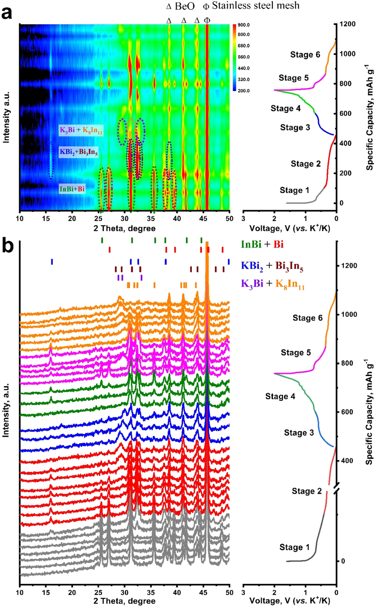
Conclusions
In summary, we fabricated the np-InBi alloy by chemical dealloying of the Mg-In-Bi precursor. The np-InBi alloy exhibits a three-dimensional ligament-channel structure with the average ligament size of 279.0 ± 70.8 nm (based upon the SEM results). As an anode for SIBs, the np-InBi anode shows the initial discharge capacity of 474.6 mAh g−1 with the ICE of 89.8%. Even in PIBs, the np-InBi anode could display the initial discharge capacity of 458.8 mAh g−1. By utilizing the operando XRD, the (de)sodiated/(de)potassiated mechanisms (crystalline products) of np-InBi were proposed, involving the (de)alloying processes of InBi + Bi ↔ NaBi + In + Na15In27 ↔ Na3Bi + Na15In27 ((de)sodiation) and InBi + Bi ↔ KBi2 + Bi3In5 ↔ K3Bi + K8In11 ((de)potassiation). The present results could provide valuable information on understanding of electrochemical processes and design of advanced alloy anode materials for SIBs and PIBs.
Acknowledgments
The authors gratefully acknowledge financial support by the National Natural Science Foundation of China (51871133), Taishan Scholar Foundation of Shandong Province, the Key Research and Development Program of Shandong Province (2021ZLGX01), and the program of Jinan Science and Technology Bureau (2019GXRC001).
Supplementary data (3 MB DOCX)