

Abstract
The present study used chemical deposition to deposit thin copper aluminum tin sulfide (CATS4) layers onto clean glass substrates. X-ray diffraction analysis was utilized to explore the crystalline structure of the CATS4 films, which refers to the CATS4 films having a cubic crystal structure. Energy-dispersive X-ray analysis showed the presence of Cu, Al, Sn, and S peaks in the CATS4 films, and their atomic ratio is close to 1:1:1:4. Spectrophotometric measurements of optical transmittance and reflectance spanning the 400–2500 nm spectral range were performed to describe the optical properties of the CATS4 layers. The CATS4 films demonstrated a direct energy gap transition between 1.42 and 1.31 eV. Further, increasing the layer thickness enhanced the refractive index and Urbach energy of the CATS4 films. The inspected CATS4 films showed better optoelectrical properties with increasing thickness, including improved optical conductivity, optical resistivity, optical carrier concentration, relaxation time, and optical mobility. Increasing the thickness of the CATS4 films increased their nonlinear optical indices. Additionally, the hot probe apparatus verified the p-type semiconducting characteristics of CATS4 films.
Export citation and abstract BibTeX RIS
Chalcogenide materials based on selenium, tellurium, and sulfur have been investigated, created, and employed for photovoltaic cells. 1–3 The inexpensive production technique, significant absorption coefficient, and direct band gap of these chalcogenide materials make them appropriate for photovoltaic applications. 4 The chalcogenide materials developed for PV applications include CuInGaSe2 (CIGS) and CdTe, which display good performances in solar cells. 5 Strong absorption coefficients mark these films, direct band gaps, and active absorber layer thicknesses of 800 nm and 2 μm, respectively. 6 For CdTe and CIGS, respectively, they have been commercialized and have obtained PCEs of 20% and 21.7%. 7,8 These layers were formed of high-cost elements such as tellurium in CdTe and indium and CIGS, which is another drawback. As a result, it is necessary to find materials with comparable qualities made of abundant components and inexpensive cost. 9
Quaternary sulfur chalcogenides (QSC) are the main target of recent articles due to their notable electrical, optical, and optoelectrical properties, including their moderate electrical resistance, excellent absorption coefficient, and suitable energy gap. 10–12 QSC materials like Cu2ZnSnS4, CuInSnS4, CuInGeS4, Ag2ZnSnS4, CuGaGeS4, Cu2NiSnS4, and Cu2CoSnS4 display good performance on the photovoltaic applications. 13,14
It has been researched to employ copper zinc tin sulfide (CZTS), which is also known by the name kesterite and has a crystal structure comparable to CIGS (chalcopyrite), as a good absorber layer in photovoltaic applications. 15,16 It comprises elements common on Earth and has an ideal band gap (1.5 eV) and a significant absorption coefficient of about 104 cm−1. These characteristics make the CZTS compound a solid rival to CIGS and CdTe devices. 17,18 The Cu2ZnSnS4 solar cell displays power efficiency magnitudes of 11.6%. 19 The efficiency of Cu2NiSnS4 solar cells based on spray pyrolysis is up to 11.34% in 2019. 20 To improve the efficiency of the Cu2ZnSnS4 solar cell, sulfur was entirely or partially substituted by selenium. The CZTSSe solid solution's 12.6% PCE value had previously held the record for the material's greatest reported efficiency until Zhou et al. recently set a new benchmark with a 13.2% PCE value for a lithium-doped kesterite device. 21 The device's significant open circuit voltage (Voc ) deficit is the cause of this restriction. High secondary phase production rates, suboptimal band alignment at the p-n junction, band tail development, and defects in the bulk are all considered to cause the significant Voc deficit. 22
Several techniques were used to grow Cu2ZnSnS4 thin films. The pulsed laser deposition method 23,24 produces good-quality films at low temperatures and is appropriate for the deposition of layers with excellent stoichiometry. Preparing these films using thermal evaporation 25,26 is straightforward and controlled. Still, it has some issues, including low yield, difficulty controlling the ratio of layers, vacuum conditions, and material waste. Owing to the impact of the electric field, which limits the dimension of the work pieces to be deposited, it has major disadvantages. 27 On the other side, electrodeposition is important technique for preparing the CZTS films with the least amount of thermal stress remaining between the coating and slide. 28,29 CZTS films can be deposited using straightforward chemical bath deposition (CBD). 30 This method has the benefit of being simple, quick, economical, and low-temperature, which results in less energy use. Still, it has drawbacks such as reproducibility, traces of deposits, masking, and issues with chemicals with varying precipitation rates. 31 Elradaf et al. successfully prepared the CuInSnS4 thin films using a simple spray system with good electrical conductivity, nonlinear optical indices, narrow band gap, and significant absorption coefficient. 32
Moreover, Hameed et al. Fabricate the CuInGeSe4 films and Si/CuInGeSe4 heterojunction by thermal evaporation. These films display an excellent refractive index, high extinction coefficient, solar efficiency of 3.37%, and a small energy gap. 33 The previous studies focused on CuInGeS4, AgGaGeS4, CuGaGeS4, CuInSnS4, and CuInGeSe4 layers, but we didn't find any article that presents CATS4 films. So, the authors in this work focused on presenting a complete study of the optical properties, structural, optoelectrical, and nonlinear optical properties of the CATS4 layers.
Experimental
This study used chemical bath deposition to generate CATS4 layers. Four solutions interacted to form the CATS4 layers. Meanwhile, 15 ml of 0.1 M CuCl2 were combined, and 45 ml of 0.3 M thiourea (SC(NH2)2) were stirred for five minutes. Then, the mixture was stirred for five minutes with 15 ml of 0.1 M Al (No3)3. Finally, 15 ml of 0.1 M SnCl2 was added to the mixture and stirred for half an hour. The pH of the CATS4 solution equal 10. After being cleaned, the glass substrates were put in the beaker at different times (4, 8, 12, and 16 h). The Bruker-Dektak XT stylus profiler was utilized to find the thickness of the CATS4 sheets, which equals 263, 317, 392, and 459 nm. Additionally, the optical data of the CATS4 sheets were identified using Shimadzu's (UV-3600 Plus UV–vis-NIR spectrophotometer). Meanwhile, a Quanta-FeG-250 USA scanning electron microscope (FESEM) was employed to evaluate the CATS4 coatings' surface morphology.
Results and Discussion
XRD study
The results of the XRD study for the inspected CATS4 films are provided in Fig. 1. These diagrams reveal the cubic CATS4 crystal structure, which agrees with the JCPDS 47–1343. The identified peaks coincided with the (222), (224), (400), (422), and (731) crystallographic planes. Additionally, using these relationships, the structural indices of the CATS4 layers have been evaluated: 34–36


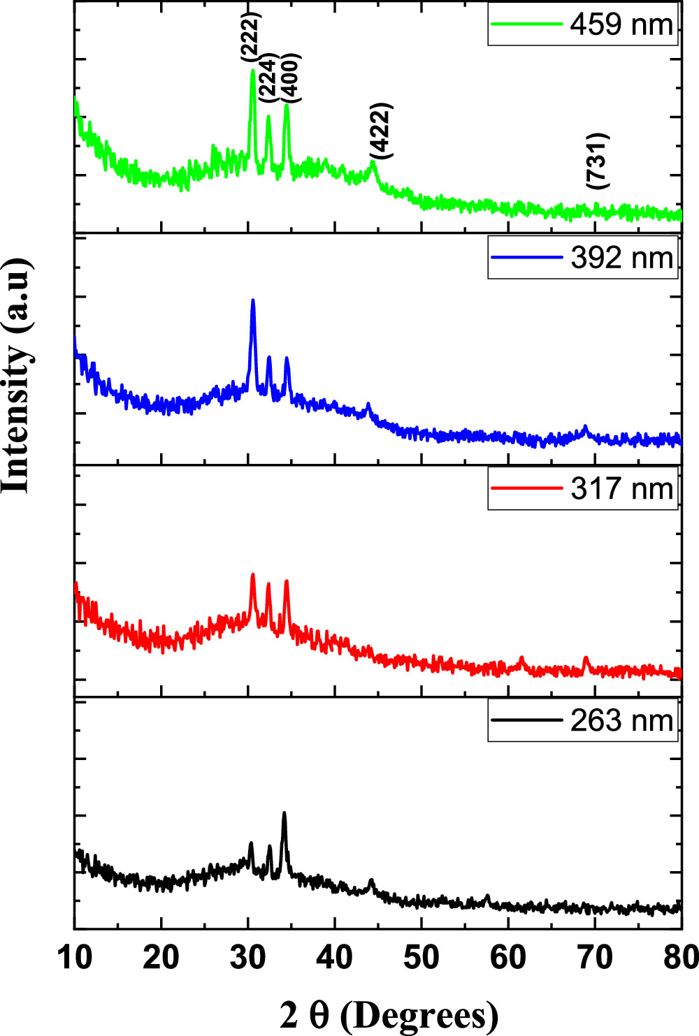
Figure 1. XRD of the CATS4 films.
Download figure:
Standard image High-resolution imageIn these relations, θ indicates the Bragg diffraction angle, D stands for the crystallite size of the CATS4 layers, and β for the experimental full width at half maximum (FWHM).
The CATS4 structural characteristics are listed in Table I. It can be noted that when the layer thickness of these samples grew, the D magnitudes of the CATS4 layers improved, and the NC of the CATS4 layers diminished. Figure 2 presents the plot of D, NC , δ, εs , and t for the CATS4 layers. Based on this graph, we concluded that expanding sheet thickness will boost the D while dropping the NC , εs , and δ values.
Table I. Structural indices of the CATS4 films.
| t (nm) |


|


|


|

|
|---|---|---|---|---|
| 263 | 28.41 | 11.47 | 1.24 | 1.22 |
| 317 | 34.31 | 7.84 | 0.84 | 1.01 |
| 392 | 41.17 | 5.61 | 0.58 | 0.84 |
| 459 | 48.42 | 4.04 | 0.42 | 0.71 |

Figure 2. (a) Plot of D of the CATS4 layers vs t, (b) Plot of εs of the CATS4 layers vs t, (c) Plot of δ of the CATS4 sheets vs t, (d) Plot of NC of the CATS4 layers vs t.
Download figure:
Standard image High-resolution imageMorphology examination
The EDX spectra of the CATS4 layers appear in Figs. 3a and 3c. It is clear that Cu, Al, Sn, and S peaks were found in the CATS4 layers, and their atomic ratios are approximately 1:1:1:4. Furthermore, the FESEM technique was used to analyze the surface of the CATS4 layers, as appears in Figs. 3b and 3d. It can be noted that the surfaces of the CATS4 samples are homogeneous and uniform.

Figure 3. (a) EDX results of the 263 nm CATS4 film, (b) SEM of the 263 nm CATS4 film, (c) EDX results of the 459 nm CATS4 film, and (d) SEM of the 459 nm CATS4 film.
Download figure:
Standard image High-resolution imageOptical properties
The optical transmittance, T, and reflectance, R, of the CATS4 layers were used to estimate the values of the linear optical indices. Figures 4a and 4b illustrate the relationships between T and R of the fabricated CATS4 layers with λ. It is evident that the increment in film thickness improves the R values of the fabricated CATS4 layers and reduces the T values of the fabricated CATS4 layers.
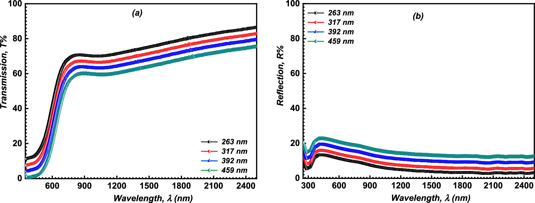
Figure 4. (a ) T vs. λ for the inspected CATS4 sheets; (b) R vs. λ for the inspected CATS4 films.
Download figure:
Standard image High-resolution imageBased on the T and R data, the absorption coefficient of the CATS4 layers is estimated through the subsequent Eq: 37–39
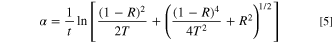
Figure 5a describes the of the α of the CATS4 layers with the λ and film thickness. It is noticeable that the values of α of the CATS4 layers are increased by expanding the film thickness. This performance agrees with other semiconductor materials. 40
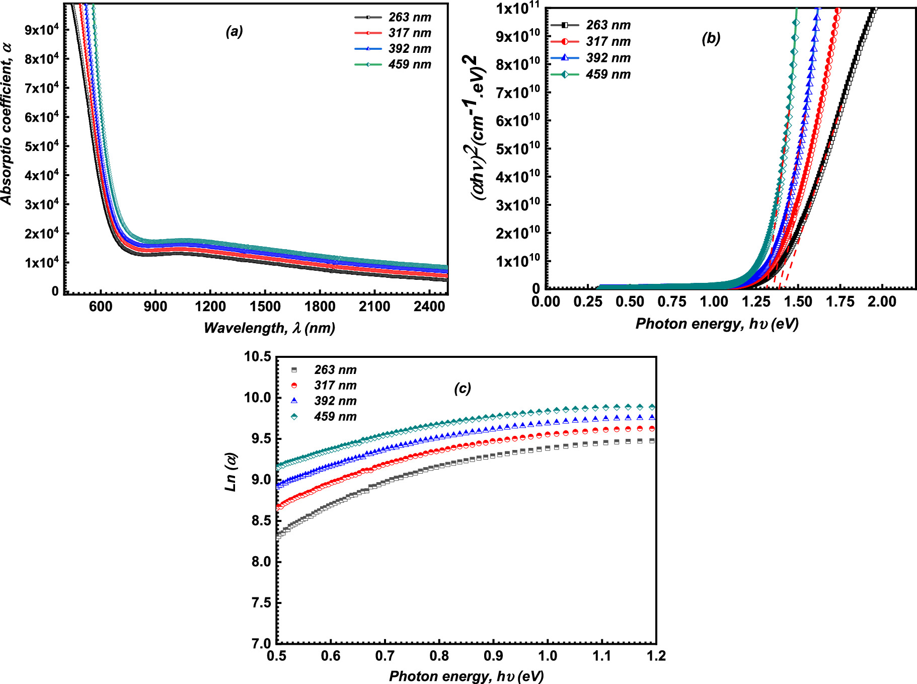
Figure 5. (a) Plot of α for the CATS4 films vs λ, (b) Tauc's plot of the CATS4 layers, (c) The Urbach graph of the CATS4 layers.
Download figure:
Standard image High-resolution imageFurthermore, the energy gap (Eg ) of the CATS4 layers could be calculated through the Tauc's relations: 41,42

Here, h detects the kind of optical transition of the CATS4 layers. It may be indirect at h = 2 or direct at h = 0.5. and P is a constant.
In this relation, h denotes the type of optical transition directly allowed (h = 1/2) or indirectly allowed (h = 2), and P is a constant. Figure 5b depicts the relationship between the photon energy and αhv of the CATS4 layers. It can be estimating the Eg values of the CATS4 layers from the intercepts with the x-axis of this plot. According to Table II, the direct Eg values of the CATS4 layers decreased from 1.42 eV to 1.31 eV. This trend related to the emergence of localized states within the gap was the cause of this tendency. 43,44
Table II. The linear optical indices and dispersion parameters of the CATS4 samples.
| t (nm) |

|

| Ed (eV) | Eo (eV) | no | εs | f |
|---|---|---|---|---|---|---|---|
| 263 | 1.42 | 0.12 | 15.39 | 2.87 | 2.52 | 6.36 | 44.16 |
| 317 | 1.39 | 0.13 | 16.57 | 2.81 | 2.62 | 6.89 | 46.57 |
| 392 | 1.35 | 0.15 | 17.28 | 2.73 | 2.71 | 7.32 | 47.19 |
| 459 | 1.31 | 0.17 | 19.14 | 2.64 | 2.87 | 8.25 | 50.52 |
Conversely, the Urbach energy (Eu ) of the CATS4 layers is evaluated through the subsequent expressions: 45,46

Figure 5c illustrates the relationship between the photon energy and ln (α) of the CATS4 layers. The Eu values of the CATS4 layers can be estimated from the slope of this plot. On the other hand, the Eu values of the fabricated CATS4 layers can be observed in Table II. It seems that the CATS4 sheets' Eu expanded along with their thickness. This trend was linked to a rise in localized states as thickness increased. 47
Furthermore, the following relation could be used to compute the refractive index (n) of the fabricated CATS4 layers: 48,49

Figure 6a describes the refractive index (n) alteration as a function of λ. It is noticeable that the increment in film thickness improves the n values of the fabricated CATS4 layers. This performance may be related to enhanced R values by expanding the layer thickness. 50–52
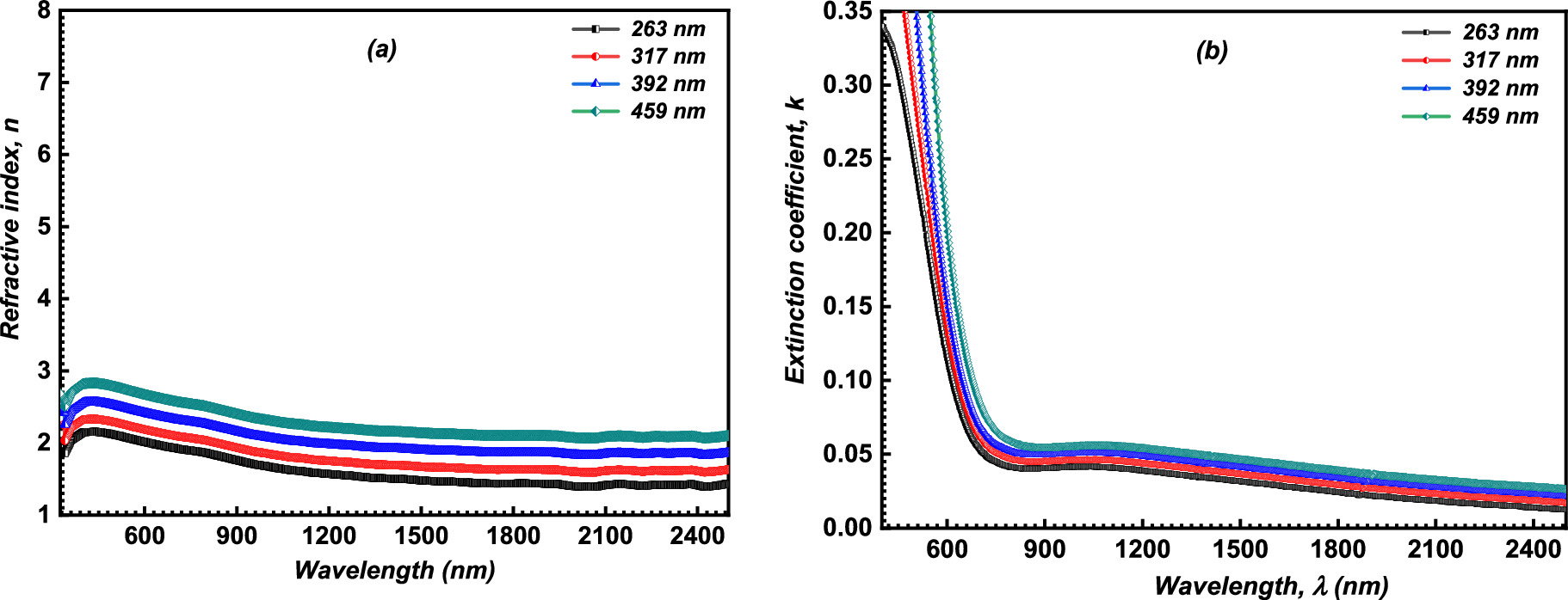
Figure 6. (a) Plot of n of the CATS4 sheets vs. λ; (b) The k of the CATS4 films against λ.
Download figure:
Standard image High-resolution imageMoreover, to deduce the extinction coefficient, k, of the fabricated CATS4 layers, the following relationship was used: 53,54

Figure 6b reveals the variation of the extinction coefficient, k, of the fabricated CATS4 layers with λ. Expanding the layer thickness improved the estimated k values of the fabricated CATS4 layers. These results agree with other chemically deposited semiconductor materials. 55,56
Also, the dispersion indices of the fabricated CATS4 layers are estimated through the subsequent expression: 57,58

Here, Eo demonstrates the oscillator energy, and Ed presents the dispersion energy of the fabricated CATS4 layers.
The correlation between  and
and  of the fabricated CATS4 layers can be observed in Fig. 7. The slopes and intercepts of the curves' straight lines yield the magnitudes of Eo
and Ed
for the fabricated CATS4 sheets (see Table II). Increasing the layer's thickness lowers the estimated magnitudes of Eo
and enhances the estimated magnitudes of Ed
of the fabricated CATS4 sheets.
of the fabricated CATS4 layers can be observed in Fig. 7. The slopes and intercepts of the curves' straight lines yield the magnitudes of Eo
and Ed
for the fabricated CATS4 sheets (see Table II). Increasing the layer's thickness lowers the estimated magnitudes of Eo
and enhances the estimated magnitudes of Ed
of the fabricated CATS4 sheets.
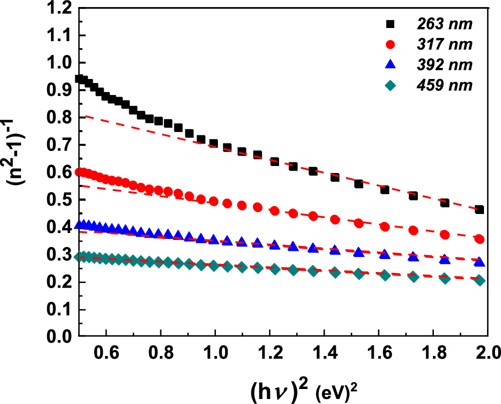
Figure 7.
 against of
  for the inspected CATS4 films.
Download figure:
Standard image High-resolution imageConversely, the high-frequency dielectric constant εs , oscillator strength f and static refractive index no of the fabricated CATS4 sheets are assessed using the following formulas: 59–61


The CATS4 layers' εs , no, and f magnitudes are given in Table II. It is evident that the improvement in εs , no, and f coincided with the thickness expansion.
Optoelectrical parameters
The optoelectrical indices of the fabricated CATS4 sheets are estimated through the subsequent relations: 62,63


In these relations,  denotes the plasma frequency, c stands for the light speed,
  refers to the lattice dielectric constant, ε0, stands for the free space's electric permittivity, e stands for the electronic charge, and
  stands for the charge carrier concentration.
In Fig. 8a, the relationship between  and
and  of the fabricated CATS4 layers is illustrated. We can estimate the
  and
and  values of the CATS4 layers from this plot. The
  and
and  values of the fabricated CATS4 layers can be observed in Table III. According to this table, the increment in film thickness produces an improvement in the
  and
and  values of the fabricated CATS4 layers due to a boost in charge carrier concentration. Moreover, the increment in film thickness produces a decrease in
  magnitudes.

Figure 8. (a)  of the inspected CATS4 films vs
  (b) Plot of ε2
vs
(b) Plot of ε2
vs  for the inspected CATS4 films.
Download figure:
Standard image High-resolution imageTable III. The optoelectrical indices of the CATS4 layers.
| t (nm) |


|

|


|


|

 Hz Hz |


|
|---|---|---|---|---|---|---|
| 263 | 1.12 | 4.98 | 14.96 | 1.51 | 4.49 | 0.06 |
| 317 | 1.45 | 5.19 | 9.08 | 3.36 | 4.41 | 0.09 |
| 392 | 1.87 | 5.46 | 8.46 | 5.68 | 4.02 | 0.23 |
| 459 | 1.94 | 5.54 | 2.56 | 6.74 | 3.69 | 0.28 |
Likewise, the relaxation time τ of the fabricated CATS4 layers is estimated through the subsequent expression: 64,65

Figure 8b describes the alteration in the ε2 of the fabricated CATS4 layers versus λ3 . The values of the relaxation time τ can be estimated from the slope of this plot. It is noticeable that the increment in film thickness produces a reduction in the values of the relaxation time τ.
On the other side, both the optical resistivity and mobility of the fabricated CATS4 sheets are predicated on the relations: 66,67


Table III shows the estimated values of μopt and ρopt for the fabricated CATS4 layers. It is noted that, by the increment in film thickness, the calculated μopt and ρopt improved. 60
Additionally, the electrical conductivity (σe ) and the optical conductivity (σopt ) of the fabricated CATS4 layers are predicated through the subsequent expressions: 68


In Fig. 9a, the relationships between σopt of the fabricated CATS4 layers with photon energy are illustrated. It is noted that the improvement in σopt coincided with enlarging the photon energy and the layer thickness. This trend related to improving the electronic charge excitation is brought about by expanding the hv. The relationship between σe of the fabricated CATS4 layers and photon energy can be observed in Fig 9b. According to this plot, the increment in the photon energy and film thickness produces an improvement in the σe values.

Figure 9. (a) The  of the inspected CATS4 films against
  (b) The
  of the inspected CATS4 films versus the
  .
.
Download figure:
Standard image High-resolution imageLikewise, to deduce the  of the fabricated CATS4 layers, the following relationships were used:
69–71
of the fabricated CATS4 layers, the following relationships were used:
69–71


Figures 10a and 10b describes the alteration in the ε1 and ε2 as a function of λ. It is evident that the increment in film thickness improves the ε1 and ε2 values of the fabricated CATS4 layers. This performance may be related to enhancing the n and k values of the fabricated CATS4 layers by the thickness growth.

Figure 10. (a) The ε1 vs λ for the inspected CATS4 films, (b) The ε2 vs λ for the inspected CATS4 layers.
Download figure:
Standard image High-resolution imageNonlinear optical characteristic
In this work, Miller's relationships could be exploited to evaluate the nonlinear optical indices of the fabricated CATS4 layers as follows: 72,73


Figures 11a–11c describes the 
 and
and  dependence on photon energy and layer thickness for the fabricated CATS4 layers. The increase in film thickness produces an enhancement in the values of the
 and
and  This trend is attributed to the growth of the refractive index of the fabricated CATS4 sheets.
74,75
This trend is attributed to the growth of the refractive index of the fabricated CATS4 sheets.
74,75

Figure 11. (a)–(c): The 
 and
and  of the inspected CATS4 sheets against
  .
.
Download figure:
Standard image High-resolution image
Hot-probe instrument of the CATS4 films
The hot probe approach indicates that the CATS4 films exhibit p-type conductivity. A sensitive multimeter and a soldering iron were the instruments employed in this process. The multimeter's positive terminal was connected to the heated side of the CATS4 film, and its negative terminal was connected to its cold side. The voltage sign in the multimeter can be used to assess whether the film is more likely to be n-type or p-type. The film inclination will be an n-type semiconductor if a positive indication is seen. On the other hand, a p-type semiconductor will be the film inclination if a negative sign is detected. 76 In our studies, all CATS4 films produce a negative voltage when the heated probe is used. The hot probe validates the films' propensity to function as p-type semiconductors.
Conclusions
Herein, the authors successfully produced CATS4 films of various thicknesses using the chemical bath deposition technique. The XRD measurements of the examined CATS4 layers demonstrate the polycrystalline and cubic structure of the inspected CATS4 films. The investigated CATS4 layers' EDAX analyses show a stoichiometric composition. By increasing the thickness of the sample from 263 to 459 nm, the direct energy gap in the CATS4 layers under investigation was lowered from 1.42 to 1.31 eV. Moreover, increasing the layer thickness enhances the refractive index and Urbach energy. Conversely, the optoelectrical characteristics of the studied CATS4 films, such as their optical resistivity, optical carrier concentration, optical mobility, relaxation time, and optical conductivity, enhanced as their thickness grew. Raising the layer thickness raised the CATS4 films' nonlinear optical indices. The examined CATS4 layers displayed p-type semiconductor characteristics using the hot probe apparatus.
Acknowledgments
I. M. Elradaf: Conceptualization, Methodology, Formal analysis, Resources, Writing, Data curation, original draft, Review & editing, H. Y. S Al-Zahrani: Conceptualization, Methodology, Formal analysis, Resources, Writing, Data curation, original draft, Review & editing. The datasets generated during the current study are available from the corresponding author on request. The authors declare that they have no conflict of interest.