
Abstract
This study investigates the effects of TMAH treatment on 5 μm-sized GaN-based Micro LEDs. Compared with untreated GaN Micro LEDs, the optical output power and external quantum efficiency of TMAH treated Micro LEDs are significantly improved. These results can be attributed to the formation of microstructures on the sidewall of Micro LEDs through the TMAH treatment and the effective light reflection is therefore constructed. This research not only improves the characteristics of LEDs, but also paves the way for green and advanced optoelectronic devices.
Export citation and abstract BibTeX RIS

This is an open access article distributed under the terms of the Creative Commons Attribution Non-Commercial No Derivatives 4.0 License (CC BY-NC-ND, http://creativecommons.org/licenses/by-nc-nd/4.0/), which permits non-commercial reuse, distribution, and reproduction in any medium, provided the original work is not changed in any way and is properly cited. For permission for commercial reuse, please email: permissions@ioppublishing.org.
GaN (gallium nitride) Micro LED (light-emitting diode) technology has emerged as a significant breakthrough in the semiconductor lighting and display industry in recent years. By combining gallium nitride semiconductor materials with tiny LED structures, GaN Micro LED brings revolutionary improvements to display and lighting applications. Given the extremely small size of GaN Micro LED, typically in the range of micrometers or sub-micrometers, the characteristics of the surface and sidewalls are crucial for its light-emitting and electrical properties. Sidewall treatment is demonstrated to improve sidewall smoothness, surface energy, and light extraction efficiency and therefore ensures effective light emission from GaN Micro LED. 1–4 Sidewall treatment techniques typically involve both dry and wet processes. Dry treatments, such as plasma etching, are employed to remove surface defects and enhance surface smoothness. Wet treatments utilize chemical solutions, such as alkaline or acidic solutions, to improve surface energy and light extraction efficiency. These sidewall treatment techniques improve the optical performance of GaN Micro LED, increasing brightness and uniformity while reducing photon reflection and absorption losses within the material. In recent years, GaN micro-LEDs have emerged as a breakthrough technology in semiconductor lighting and display. Many scholars have also proposed strategies for the sidewall treatment of GaN micro LEDs, including the use of potassium hydroxide (KOH), 5–10 hydrofluoric acid (HF), 11–15 tetramethylammonium hydroxide (TMAH), 16–19 ALD deposition enhanced passivation layer Intensity (Al2O3, AlN) 20–22 and distributed Bragg reflector (DBR) structures to increase reflectivity. 23–30
TMAH is an alkaline solution with excellent etching capabilities and selectivity, making it suitable for removing unwanted materials and improving optical characteristics of the GaN Micro LED. Due to its high selectivity towards GaN material, TMAH can precisely remove metal electrodes and unwanted materials while preserving the integrity of the GaN Micro LED structure. Furthermore, TMAH can improve the optical characteristics of GaN Micro LED. In some cases, there may be defects or surface non-uniformities present within the GaN Micro LED structure, which can impact photon emission and light extraction efficiency. Therefore, in the study, we provide an effective way to enhance the optical performance of GaN LED using TMAH treatment by removing defects and then improving the reliability of the GaN Micro LEDs.
Experimental
A metal–organic chemical vapor deposition (MOCVD) system was used to grow GaN-based blue LEDs on a 4-inch sapphire substrate. The LED epilayer consisted of several layers, including an undoped Gallium nitride (GaN) buffer layer, a Si-doped n-GaN layer, a 15-pair multiple quantum wells (MQWs) of InGaN/GaN, and a p-GaN layer, as shown in Figs. 1a and 1b. To create a mesa structure, an inductively coupled plasma (ICP) etching system was employed to construct a mesa depth of about 0.8 μm and a mesa size of 5 μm. After the mesa process was completed, the device underwent sidewall treatment by being soaked in TMAH with a concentration of 2.38 and a temperature of 60 °C for 10 min. The passivation layer was formed by depositing 125 Å of Al2O3 using ALD, followed by the deposition of 3000 Å of SiO2 for sidewall cladding insulation by PECVD. The passivation layer was then prepared using photolithography process and dry etching by ICP. Subsequently, a 60-nm-thick ITO transparent conductive layer was evaporated onto the p-GaN layer. To form the p- and n-electrodes, multilayers of Cr/Pt/Au (20 nm/50 nm/2 μm) were deposited on the ITO and n-GaN layers. Micro LED array was also realized to demonstrate the effect of TMAH treatment on the performance of Micro LEDs and the SEM image of the Micro LED array is displayed in Fig. 1c. Figure 1d illustrates the luminous condition of the 5 μm-sized Array, and Fig. 1e presents the luminous state of the array after bonding to the circuit board and being illuminated.
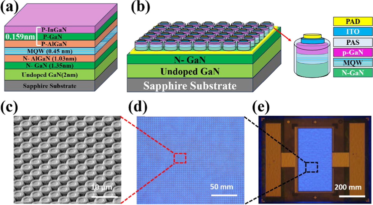
Figure 1. (a) Schematic illustration of GaN-based LED epitaxial structure. (b) Schematic structure of GaN Micro-LED. (c)SEM image of Micro LED array. (d) GaN Micro-LED Illumination Image. (e) Bonding schematic for GaN Micro-LED.
Download figure:
Standard image High-resolution imageThe study investigated the material properties of Micro LEDs with citric acid sidewalls using different techniques. Initially, the surface characteristics of the microstructures were analyzed using a field emission scanning electron microscope (FE-SEM, FEI Quanta 400) at 15 kV. Subsequently, on-wafer Micro LEDs were tested to evaluate their current-voltage (I-V) performance and light-output power. This evaluation is constructed by a probe station equipped with an integrating sphere and spectrometer. To streamline the measurement process, the Micro LEDs on the entire wafer were arranged in a 4 × 4 array and bonded onto a custom-made circuit board. This bonding ensured an effective encapsulation of the Micro LEDs, allowing for the comprehensive collection of isotropic light in the integrating sphere. Consequently, crucial parameters such as forward voltage, wavelength, output power, wall-plug efficiency (WPE), and external quantum efficiency (EQE) could be determined for different current densities applied to the Micro LEDs.
Results and Discussion
Figure 2 depicts the variations in the sidewall surface of Micro LEDs after immersion in TMAH solutions for 0 min and 10 min. Figures 2a and 2b show SEM images of untreated Micro LEDs at 10× and 50× magnification, respectively. As the TMAH treatment duration increases, the rough surface of Micro LEDs is observed, as displayed in Figs. 2c and 2d with 10× and 50× magnification, respectively.

Figure 2. SEM images at two magnifications (top row: 10×, bottom row: 50x) for untreated (2a), (2b) and treated (2c), (2d) Micro LEDs.
Download figure:
Standard image High-resolution imageWith the reduction in chip size, dry etching technology faces significant challenges in semiconductor manufacturing processes. Dry etching is a process that utilizes gaseous chemicals to remove materials and is commonly used in chip fabrication. However, this method may cause damage to the chip's surface and sidewalls. Especially as chip sizes decrease, the sidewall defects induced by dry etching become more pronounced, potentially leading to an increase in leakage current. For Micro Light-Emitting Diodes (Micro LEDs), this situation is particularly crucial. While surface roughening can increase the refractive index, thereby enhancing light emission efficiency, this gain might be offset by damage caused to Micro LED sidewalls during the dry etching process. Sidewall damage results in efficiency reduction, limiting the overall improvement in light emission efficiency. Therefore, the search for gentler or more precise etching methods is crucial for enhancing Micro LED performance, especially in applications aiming for higher light emission efficiency and lower leakage current. We also list relevant literature to explain the impact of chemical treatment and surface roughening on LED characteristics.
The current-voltage characteristics of Micro LEDs with and without TMAH treatment are depicted in Fig. 3. At a current density of 20 A cm−2, the forward voltages for the untreated and 10-min TMAH treated are 2.7 V and 2.9 V, respectively. Compared with the untreated sample, the forward voltage of the TMAH-treated device increased slightly by 0.2 V. However, these increments are considered acceptable, suggesting that TMAH only induces a marginal impact on the device characteristics. The main objective of the experiment was to enhance the brightness extraction in micro-LEDs with small emitting areas.

Figure 3. Voltage of red Micro LED with and without TMAH treatment.
Download figure:
Standard image High-resolution imageFigure 4 illustrates the light output power of the red Micro LED under continuous operation at an injected current density of 50 A cm−2. At a current density of 50 A cm−2, the light output power for the untreated and 10-min TMAH treated samples are 2.38 μW and 3.23 μW, respectively. After TMAH treatment, the light output power can effectively increase. Figure 5 illustrates the relationship between the external quantum efficiency (EQE) and current density for GaN Micro LEDs with and without TMAH treatment. At a current density of 50 A cm−2, the EQE values for the untreated and 10-min treated TMAH samples are 11.65% and 12.41%, respectively. Compared to the untreated GaN Micro LED, the EQE is enhanced by 6.1% for the 10-min TMAH treatments LED. The TMAH-treated Micro LEDs exhibit an increasing EQE with the rise in current density. This behavior can be attributed to the microstructures formed on the sidewalls, and therefore effectively enhance the light reflection and increase the EQE. Wall-plug efficiency (WPE) is defined as the ratio of the visible light energy produced by the LED light source to the input electrical energy. It represents the efficiency of electrical energy converted into visible light. For the energy not successfully converted into light is transformed by heat. Figure 6 displays the relationship between the WPE and current density for GaN Micro LEDs subjected to different TMAH treatments: no etching and 10-min etching. At a current density of 50 A cm−2, the WPE values for the untreated and 10-min TMAH treated samples are 10.99% and 10.44%, respectively. Compared to the untreated GaN Micro LED, the WPE for TMAH treated Micro LEDs is reduced by 5.0%. Based on the results, it can be observed that the TMAH-treated devices exhibit higher energy conversion into heat during the conversion process. According to the observations from Fig. 3, it can be noted that micro light-emitting diode (LED) treated with TMAH exhibit an increase in forward voltage as the current density rises. This phenomenon may be attributed to microstructures formed during the TMAH treatment in the Micro LED manufacturing process, leading to the generation of leakage current paths and subsequently raising the internal temperature of the components. The Wall Plug Efficiency (WPE) is used to assess the efficiency of converting electrical energy to light energy. Examining the data from Fig. 6, TMAH-treated LEDs show a decrease in light conversion efficiency, possibly due in part to an increase in non-radiative recombination, 9 further leading to an increase in internal heat, indicating more energy being converted to heat rather than light, resulting in reduced efficiency. To address these issues, future research should focus on developing more effective passivation layers or adopting multilayer epitaxy techniques and other treatment methods to minimize component damage. This can effectively enhance the performance of the components, reduce leakage current and non-radiative recombination, thereby improving the overall luminous efficiency and stability. These optimization strategies are crucial for enhancing the performance of Micro LEDs after TMAH treatment, contributing to their competitiveness in various applications.

Figure 4. Light output power of red Micro LEDs with and without TMAH treatment.
Download figure:
Standard image High-resolution image
Figure 5. External quantum efficiency of red Micro LEDs with and without TMAH treatment.
Download figure:
Standard image High-resolution image
Figure 6. WPE of red Micro LED with and without TMAH treatment.
Download figure:
Standard image High-resolution image
Through the analysis of Figs. 4 and 5, it is observed that as the current density of Micro LED components reaches 20 A cm−2, the accumulated heat within LEDs gradually increases. With further increases in current density, a decreasing trend is observed in both light output power and external quantum efficiency (EQE). This phenomenon can reasonably be attributed to thermal impacts caused by rapid current changes and higher current density, potentially leading to structural changes in the material. These structural changes may have a negative impact on the overall performance of Micro LEDs, especially in terms of forward voltage behavior. As internal heat accumulates in LEDs, it may result in an increase in non-radiative recombination 1–4,9 and a decrease in light output efficiency, thereby affecting the overall efficiency of the components.
Conclusions
In the work, we propose a strategy to construct a light reflection microstructure on the sidewall of Micro LEDs through the TMAH treatment. TMAH treatment plays a vital role in optimizing the performance of GaN-based micro-LEDs. After TMAH treatment, both the optical output power and the external quantum efficiency increase. Additionally, we observe variations in external quantum efficiency and wall-plug efficiency under different treatment conditions, emphasizing the appropriate treatment duration could effectively improve the performance of Micro LEDs. The outcomes of this study offer valuable insights for enhancing GaN-based Micro-LEDs and provide a valuable reference for related research and applications.
Acknowledgments
This work was supported in part by the National Science and Technology Council of Taiwan, ROC, under the grants MOST 110–2221-E-168–001-MY3, MOST 111–2221-E-168–001-MY3, NSTC 112–2222-E-006–011-MY2, NSTC 112–2222-E-218–002, NSTC 112–2622-E-168–001and NSTC 112–2221-E-168–005 and in part by the Green Energy Technology Research Center, Department of Electrical Engineering, Kun Shan University, Tainan, Taiwan, through The Featured Areas Research Center Program within the framework of the Higher Education Sprout Project by the Ministry of Education in Taiwan.