
Abstract
Heterojunction p-GaN/n-ZnO light emitting diode (LED) structure using Eu-doped ZnO (ZnO:Eu) as an active component is demonstrated in order to realize low-cost and environmentally-friendly red LEDs with sharp linewidth and temperature stability against surrounding environment including operating temperature and injection current. Chemically stable Al2O3 is inserted as an electron blocking layer between p-GaN and ZnO:Eu/n-ZnO in order to facilitate the injection of carriers into the ZnO:Eu active layer. Al2O3 insertion with a moderate thickness (∼10 nm) facilitates the carrier recombination at the ZnO layer with comparatively low resistivity. Device characteristics of the p-GaN/Al2O3/ZnO:Eu/n-ZnO LED structures show red luminescence under current injection with reversed bias voltage originated from Eu3+ ions in the ZnO host. Detailed optical characteristics of the ZnO:Eu layer in the LED structures utilizing the combined excitation emission spectroscopy measurement enable the identification of the luminescence centers contributing to Eu luminescence under both indirect excitation and collisional excitation. The luminescence center contributing to Eu luminescence under indirect excitation via the ZnO host is different from that under collisional excitation, which would pave the way to understand the Eu luminescence mechanism in ZnO:Eu, and hence realize high-brightness LED structures based on rare-Earth doped ZnO as an active component.
Export citation and abstract BibTeX RIS

This is an open access article distributed under the terms of the Creative Commons Attribution 4.0 License (CC BY, http://creativecommons.org/licenses/by/4.0/), which permits unrestricted reuse of the work in any medium, provided the original work is properly cited.
Light emitting diodes (LEDs) have garnered considerable attention as eco-friendly devices used in displays and lighting applications. After the invention of blue and green LEDs based on InGaN/GaN, full-color large-screen LED displays could be developed by combining them with the third primary color, red. For future applications in microdisplays and flexible/wearable augmented-reality devices, including head mounted displays and retinal projection displays, it is strongly desired to achieve the three primary colors on the same platform. Blue and green LEDs are well established and can be achieved by InGaN quantum wells (QWs) as the active layer. 1,2 However, although InGaN-based red LEDs have also been recently demonstrated, 3 there still exist serious limitations including a broad emission spectrum and an injection-current-dependent emission wavelength due to the internal piezoelectric field, 4 resulting in a poor external quantum efficiency of the LEDs. There have been other approaches to realize red light emission on the GaN platform including the use of nanowire/nanocolumn structures. 5,6 However, in both cases, the luminescence wavelength of these LEDs varies with injection current and operating temperature, since the luminescence mechanism of such LEDs is based on conventional band-to-band transition of electrons in the conduction band and holes in the valence band.
Eu3+-doped semiconductors can exhibit sharp red luminescence at ∼620 nm due to 4 f intra-shell transitions of Eu3+ ions. These materials can excite Eu3+ ions efficiently via the energy transfer from the host material, and can be applied to photonic devices such as light emitting diodes (LEDs) 7 and single photon emitters. 8 Our group has demonstrated efficient red LEDs based on Eu-doped GaN, and their luminescence output power has exceeded 1 mW at 20 mA with an external quantum efficiency of 3.3%, by careful optimization of the growth conditions and device designs. 9 Furthermore, three-primary color LEDs monolithically vertically stacked on the same GaN platform have been recently demonstrated by utilizing Eu-doped GaN as the red component, 10 which would provide a novel strategy to develop μ-LED displays.
ZnO is direct band-gap semiconductor whose band-gap energy is very similar (3.37 eV) and has the same hexagonal wurtzite crystal structure as GaN. ZnO has also drawn significantly practical and scientific attention as potential optoelectronic material due to its large exciton binding energy (∼60 meV), abundant material resources, inexpensive manufacturing, and environment-friendly nature. Pioneering development of p-doped ZnO 11 has accelerated diverging application in photonic devices including LEDs 11,12 and lasers, 13 since ZnO can cover the whole visible emission regime. Furthermore, hybridization of nanostructured ZnO, including nanocrystals, nanodots and nanowires, with flexible materials has enabled the realization of novel photonic nanodevices for applications in photovoltaics, 14 in-vivo biosensing 15 and medical devices due to their high biocompatibility. Therefore, it would be advantageous if ZnO materials/devices could be incorporated with Eu3+ ions and develop a material with a high color purity and extremely high temperature sensitivity. This ZnO material has, however, encountered the difficulty in realizing high-conductivity p-type ZnO, although several demonstration of the p-type ZnO has been reported, 16–18 which has hindered the commercialization of ZnO-based homojunction devices including LEDs and lasers. 19 Recently, heterojunction LEDs using dissimilar materials in p-type, especially GaN, have been attracting practical attention. In a simple p-n heterojunction of p-GaN and n-ZnO, the band offsets of both conduction and valence bands are almost the same. However, the injection of electrons into p-GaN becomes dominant due to the difference of the mobility and carrier density, and hence carrier recombination of electrons and holes predominantly takes place at the p-GaN region resulting in blue luminescence from only p-GaN emission. Therefore, it is necessary to suppress the injection of electrons into the p-GaN layer in order to obtain the luminescence from ZnO. One of the methods to realize this is to insert an electron blocking layer (EBL), whose conduction band offset is larger than the valence band offset, into the p–n junction interface. There have been several materials for the EBL between n-ZnO and p-GaN so far reported such as Al2O3, 20,21 AlN, 22 and MgO. 23 Among of these materials, Al2O3 is considered as one of the candidates because of its mature film preparation technology. Our group has so far demonstrated clear Eu luminescence from ZnO:Eu grown by sputtering-assisted metalorganic chemical vapor deposition (MOCVD). 24–28
In this contribution, the heterojunction p-GaN/n-ZnO LED structure using ZnO:Eu as the active layer is demonstrated in order to realize a low-cost and environmentally friendly red LEDs. Al2O3 is inserted as an EBL to facilitate the injection of carriers into the ZnO:Eu active layer. First, p-GaN/Al2O3/n-ZnO heterojunction LEDs are fabricated to elucidate that the carrier recombination predominantly takes place at the ZnO layer. Then the growth of the p-GaN/Al2O3/ZnO:Eu/n-ZnO LED structures are performed to characterize the device properties of the LEDs. Finally, the optical characteristics of the ZnO:Eu layer in the LED structures are performed to clarify the luminescence mechanism of Eu in ZnO by combined excitation emission spectroscopy (CEES).
Experimental
The schematic of the whole structure of p-GaN/Al2O3/ZnO:Eu/n-ZnO LEDs is depicted in Fig. 1a. Samples were grown at the following schemes on 2-inch c-plane sapphire (0001) substrates. First, a GaN template was grown by metalorganic vapor phase epitaxy (Taiyo Nippon Sanso SR-2000) utilizing Trimethylgallium (TMGa, purity: >99.99995%), ammonia (NH3, purity: >99.99997%), and bis-cyclopentadienyl magnesium (Cp2Mg, purity: >99.9999%) as Ga, N and Mg precursors. The growth process was initiated with the growth of low temperature (LT) GaN buffer, ∼1.0 μm-thick undoped-GaN (ud-GaN) and 140 nm-thick p-GaN on sapphire (0001) substrates. Next, after covering half of the GaN template with sapphire substrates, ∼10 nm-thick Al2O3 was deposited at the substrate temperature of 300 °C by using atomic layer deposition (SP560-AL, SPLEAD Inc.). The Al2O3 thickness of ∼10 nm is determined by two factors; one is the current-voltage (I–V) characteristics of the LEDs which exhibit the highest rectification ratio with moderately lower resistivity. Indeed, thinner Al2O3 (<10 nm) causes decrease in the rectification ratio while thicker Al2O3 (>10 nm) results in drastic increase in the resistivity. And another factor is the PL characteristics of the ZnO active component which has been reported in the Ref. 20 exhibiting the strongest PL intensity from the ZnO active component at the Al2O3 thickness of ∼12 nm. Trimethylaluminum and H2O were used as Al and O precursors, respectively. Finally, both of Eu-doped ZnO and n-type ZnO were grown by sputtering-assisted metalorganic chemical vapor deposition on a horizontal substrate holder with a resistive heater in a bell-jar chamber. The growth was initiated with the formation of 100 nm-thick Eu-doped ZnO layers via the thermal reaction of diethylzinc (DEZn) in O2 gas at a substrate temperature of 600 °C. Incorporation of Eu3+ ions was achieved by RF magnetron sputtering at 40 W using Eu2O3 sintered targets (5 cm diameter) that were fixed above the substrate at a 90° angle and at a distance of 12.5 cm. The DEZn and O2 flow rates were fixed at 1.11 μmol s−1 and 22.2 μmol s−1, respectively, corresponding to a VI/II ratio of 20. This growth was then followed by the formation of 85 nm-thick n-type ZnO films at a substrate temperature of 700 °C. The structural properties were characterized by scanning electron microscopy (SEM) and transmission electron microscopy (TEM: JEM-ARM200F, JEOL). The specimen for the cross-sectional TEM observation was cleaved from the as-grown LED structures into 3 mm × 1 mm × ∼430 μm sizes using a diamond saw, and polished until the 1 mm-thick specimen becomes the 100 μm-thickness with a mechanical polisher using the diamond papers (abrasive grit size: 30 and 9 μm). In addition, thinning of the 100 μm-thick specimen was performed by Argon ion milling until TEM observation area was less than ∼ several 10 nm-thickness. Then the specimen was removed from the milling and mounted on a reinforcement ring for TEM observation. The concentration of Eu in ZnO:Eu was estimated to be 0.1 at% whose details are discussed in our previous publications,
24–28
as well as Appendix

Figure 1. (a) Schematic of fabricated LED structures composed of heterojunction p-GaN/n-ZnO with an 10-nm-thick Al2O3 EBL containing 100-nm-thick ZnO:Eu layer as an active component. (b,c) Cross-sectional TEM images of (b) the whole structure and (c) interface between p-GaN and ZnO:Eu layer (enlarged area of the dashed line in Fig. 1b).
Download figure:
Standard image High-resolution imageResults and Discussion
The TEM image of the fabricated LED structure is shown in Fig. 1b, which exhibits a clear contrast from the ∼10 nm-thick Al2O3 in the vicinity of the interface between ZnO:Eu and the p-GaN layer. The closer TEM observation of the interface in Fig. 1c indicated by the dashed line of Fig. 1b reveals that the GaN matrix is composed of a single crystal while the Al2O3 layer is amorphous. By contrast, a large number of grain boundaries are observed from the ZnO:Eu layer, suggesting that ZnO is deposited in a grain configuration. In order to elucidate that the carrier recombination predominantly takes place at the ZnO layer, p-GaN/Al2O3/n-ZnO heterojunction LEDs are fabricated without doping Eu at the growth of the ZnO active region. The p-GaN/Al2O3/n-ZnO heterojunction LEDs exhibits good rectification behavior (see Appendix

Figure 2. (a) RT EL spectra of the LED structure with and without the Al2O3 EBL at an injection current of 100 μA. (b) RT PL spectra of n-ZnO and p-GaN with an excitation by He-Cd lasers (10 mW).
Download figure:
Standard image High-resolution imageNext, the device characterization of the LEDs with Eu doping to the ZnO active layer is performed. Figure 3a shows the typical RT PL spectrum of the ZnO:Eu layer embedded in the LED structure. The band edge light emission from GaN and ZnO are observed at ∼430 and ∼390 nm, respectively, while a very broad emission centered at 600–700 nm is also observed, which originates predominantly from oxygen vacancies especially on the surface of ZnO NWs. There are multiple sharp luminescence peaks from Eu3+ ions embedded in the ZnO. It is noted here that the red luminescence with the strongest PL intensity from the 5D0–7F2 transition is located between 610 and 625 nm. Several other peaks from Eu ions are also observed at 540 nm (5D1–7F1), 590 nm (5D0–7F1), and 660 nm (5D0–7F3). Figure 3b shows the RT EL spectra of the LED structure with and without the Al2O3 EBL under forward and reversed biases (30 and −30 V) at the injection current of 200 and −100 μA, respectively. In the forward bias, the band edge light emission from the ZnO is observed from the LED structures with the EBL, while very broad emission peaked at the red regime is observed from the LED structures without the EBL, which is likely originated from the yellow luminescence of the GaN layer. In both cases, no Eu luminescence is observable under the forward bias. By contrast, Eu luminescence is observed at the peak wavelength of ∼615 nm under the reverse bias, while no Eu luminescence is observable from the LEDs without the EBL. In order to clarify the behavior of such Eu luminescence, both of the PL and EL spectra in the vicinity of Eu luminescence are compared. Figure 3c shows the enlarged PL and EL spectra of the Figs. 3a and 3b, respectively in the vicinity of the 5D0→7F2 transition. The luminescence peaks are located predominantly at 613.4, 619.4 and 622.1 nm under the PL characterization, while the Eu luminescence peaks are observed at mainly 616.7 and 629.6 nm under the EL characterization with reversed bias which are totally different from those under PL characterization. In general, the PL characterization with an excitation by a He–Cd laser exhibits multiple Eu luminescence by indirect excitation of the ZnO host through the energy transfer process. By contrast, the luminescence mechanism under current injection of RE-doped semiconductors can be classified into two types: one is the indirect excitation, in which the energy caused by the recombination of electron-hole pairs in the host material is transferred to RE ions by a non-radiative process, and luminescence occurs by relaxing the electrons from excited states to the ground state. The another is a collisional excitation, where hot electrons with a large momentum collide with RE ions, and hence directly excite the electrons in the RE ions from a lower state to a higher one. Although the details are not known at the current stage, it is thought that a portion of the electrons accumulated near the interface between Al2O3 and p-GaN overcome the barrier and hot electrons are generated during the injection process into the ZnO layer when a reverse current is applied to this structure, which results in collisional excitation of the RE ions. Details of such excitation mechanism are described in Appendix
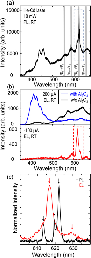
Figure 3. (a) RT PL spectrum of the p-GaN/Al2O3/ZnO:Eu/n-ZnO LED with an excitation by He-Cd laser at 10 mW. (b) (top) RT EL spectra of the LED structure with and without the EBL under forward bias at an injection current of 200 μA. (bottom) RT EL spectrum of the LED structure with the EBL under reversed bias at an injection current of −100 μA. (c) Enlarged PL and EL spectra of the black and red dashed squares in Figs. 3a and 3b, respectively in the vicinity of the 5D0→7F2 transition.
Download figure:
Standard image High-resolution imageIn order to gain more information about the difference of such luminescence mechanism especially under current injection, the CEES characterization is performed at 10 K for the LED sample with Al2O3. First, the luminescence centers which show up under indirect excitation are identified. Figure 4a shows the CEES map of the LED sample. Among all the 18 luminescence centers from Eu3+ ions in the ZnO:Eu directly grown on sapphire substrates as a reference (see Appendix
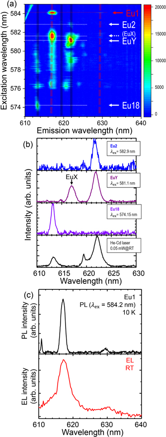
Figure 4. (a) CEES map at 10 K of the ZnO:Eu in the LED structures. (b) PL spectra at 10 K of three main luminescence centers of Eu2, EuY and Eu18 at the excitation wavelength of λex = 582.9, 581.1 and 574.15 nm, respectively, and PL spectrum with an indirect excitation by He-Cd lasers. (c) (top) PL spectrum at 10 K of the luminescence center of Eu1 and (bottom) RT EL spectrum of the LED structures with the EBL under reversed bias.
Download figure:
Standard image High-resolution imageConclusions
Heterojunction p-GaN/n-ZnO LED structure using ZnO:Eu as the active layer is proposed and demonstrated in order to realize a low-cost and environmentally friendly red LEDs. Chemically stable Al2O3 is inserted as an EBL between p-GaN and ZnO:Eu/n-ZnO to facilitate the injection of carriers into the ZnO:Eu active layer. Moderate thickness of Al2O3 (∼10 nm) in p-GaN/Al2O3/n-ZnO heterojunction LEDs enables the carrier recombination at the ZnO layer. Device characteristics of the p-GaN/Al2O3/ZnO:Eu/n-ZnO LED structures shows Eu luminescence under current injection with reversed bias voltage. Detailed optical characteristics of the ZnO:Eu layer in the LED structures utilizing the CEES measurement enables the identification of the luminescence center contributing to Eu luminescence under both indirect excitation and collisional excitation. Indeed, the luminescence center contributing to Eu luminescence under indirect excitation via the ZnO host is different from that under collisional excitation. These results would enable to understand the Eu luminescence mechanism in ZnO:Eu, resulting in the realization of high-brightness LED structures based on rare-Earth doped ZnO as an active component.
Acknowledgments
This work was partly supported by Grant-in-Aid for Scientific Research (B) (Grant No. 19H02573), Grant-in-Aid for Specially Promoted Research (Grant No. 18H05212) of the Japan Society for the Promotion of Science, Nanotechnology Platform (Grant No. JPMXP09F21OS0021 and JPMXP09S21OS0013) of the Ministry of Education, Culture, Sports, Science and Technology (MEXT), the Murata Science Foundation, the Samco Foundation, the Canon Foundation and Iketani Science and Technology Foundation.
Appendix A.: EDS Characterization
Our previous publication reveals that the concentration of Eu in ZnO:Eu is estimated to be 0.1 at% by energy dispersive X-ray spectroscopy (EDS: JEOL Ltd., EX-64175JMV) for both of secondary ion mass spectroscopy or X-ray fluorescence. 25,26 In this manuscript, the Eu concentration of ZnO:Eu is characterized by the EDS equipped in the TEM facility using the specimen prepared for the TEM observation as shown in Figs. A·1a. Figure A·1b shows the Eu concentration profile (at%) as a function of the distance from the p-GaN/Al2O3 interface. The concentration profile shows clear increase in the Eu concentration at the ZnO:Eu layer. The difference of the Eu concentration between ZnO:Eu and n-ZnO, p-GaN layers is approximately ∼0.12 at% which is almost the same order of the lower detection limit of ∼0.1 at%. The observed background of Eu concentration (∼0.1 at%) at the n-ZnO and p-GaN layers compared with the Al2O3 layer is due to unintentional doping of Eu during the growth of both ZnO and GaN. This is because our growth facilities often deal with Eu containing materials, leading to the contamination of Eu caused by the memory effect of Eu adatoms. Therefore, at this moment, the Eu concentration cannot be precisely quantified, but it can be concluded at least that there likely exist Eu ions in the ZnO:Eu layer whose concentration is approximately at the order of 0.1 at%, which is consistent with our previous publications.

Figure A·1. (a) Cross-sectional TEM images of the whole LED structures and (b) EDS spectrum intensity of Eu as a function of distance from the GaN/Al2O3 interface.
Download figure:
Standard image High-resolution imageAppendix B.: I–V Characteristics
I-V measurement is a method of measuring the current value flowing through a sample while changing the voltage. In the case of an ideal light emitting diode, the I–V characteristics between the p(n) and the p(n)-type semiconductors exhibit ohmic properties if p(n)-type dopants are properly doped into the semiconductor host, and the I–V characteristics between the p and n-type semiconductor show rectification behavior. Figure A·2a shows the I-V characteristics between p-GaN–p-GaN, n-ZnO–n-ZnO, which clearly exhibit the ohmic contact, indicating that both of p- and n- dopants are properly doped into GaN and ZnO hosts, respectively. Figure A·2b shows the I-V characteristics of fabricated p-GaN/Al2O3/ZnO:Eu/n-ZnO heterojunction LEDs with and without the Al2O3 EBL, both of which exhibit the rectification behavior with a turn on voltage of ∼4 and ∼7 V for the LEDs, respectively. Higher turn on of the LED with the EBL is owing to the existence of Al2O3 layer.
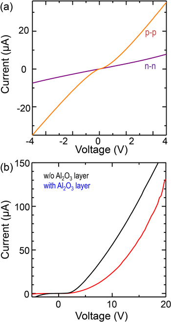
Figure A·2. (a) I-V characteristics between p-GaN–p-GaN and n-ZnO–n-ZnO. (b) I-V characteristics between p-GaN and n-ZnO of the p-GaN/Al2O3/ZnO:Eu/n-ZnO LED structure.
Download figure:
Standard image High-resolution imageAppendix C.: Mechanism of the Collisional Excitation of Eu3+ Ions in the ZnO:Eu Layers of the Fabricated LEDs
Figure A·3 shows the schematic model of the mechanism of the collisional excitation of Eu3+ ions in the ZnO:Eu layers of the fabricated LEDs under the reversed bias. The following behavior is thought to occur when a reverse voltage is applied to the fabricated LEDs:
- -Due to the application of a large reverse voltage, electrons from the p-GaN accumulate in the vicinity of the interface between Al2O3 and p-GaN which results in a population inversion.
- -Accumulated electrons tunnel into ZnO:Eu as hot electrons through the Al2O3 barrier layer owing to their strong applied electric field.
- -A portion of the hot electrons collide with Eu3+ ions in the diffusion process through the ZnO:Eu layer, and the kinetic energy of the hot electrons directly transfer to Eu3+ ions to excite the electrons to the excited state. Finally luminescence from Eu3+ ions takes place by relaxing the electrons from the excited to the ground state.

Figure A·3. Schematic model of the mechanism of the collisional excitation of Eu3+ ions in the ZnO:Eu layers of the p-GaN/Al2O3/ZnO:Eu/n-ZnO LEDs under the reversed bias.
Download figure:
Standard image High-resolution imageIn the ZnO:Eu, luminescence from both Eu3+ ions and the ZnO host is observed under indirect excitation while only luminescence from Eu3+ ions is observable under direct excitation. Therefore, obtained EL spectra under the forward bias originate from the luminescence centers contributing to Eu luminescence under indirect excitation via the ZnO host, while EL spectra under the reversed bias originate from those under direct excitation due to the collisional excitation. Further studies including the dependence of the EL intensity of Eu luminescence on the injection current are required to elucidate the mechanism of hot carrier generation, 33,34 and will be a subject of future publication.
Appendix D.: Identification of the Eu Luminescence Centers from the CEES Mapping
In the CEES measurement, the PL spectra are collected by changing the excitation wavelength using a tunable laser (in this manuscript, dye lasers), and Eu luminescence center is excited with a photon energy corresponding exactly to the 7F0–5D0 transition of Eu3+ ions. Two-dimensional mapping of excitation wavelength vs PL spectrum is obtained by observing the PL spectrum in the vicinity of the 5D0–7F2 transition. At this stage, since the 7F0–5D0 transition does not split due to the crystal field, different luminescence centers originate for different excitation energies. Therefore, it is important to investigate the luminescence mechanism of Eu ions in order to increase the intensity of Eu luminescence.
In this contribution, Eu luminescence from the LED structures is observable under current injection with reversed bias voltage due to collisional excitation. Therefore, CEES measurement is performed to analyze and identify the luminescence centers under current injection. Two types of the samples are characterized: one is the LED structure, p-GaN/Al2O3/ZnO:Eu/n-ZnO, and another is the ZnO:Eu layer directly grown on sapphire substrates as reference. From the CEES mapping, the ratio of each luminescence centers is totally different between the two structures. Figure A·4a shows the CEES mapping of the ZnO:Eu/sapphire which exhibits 18 different luminescence centers depending on the excitation wavelength which is owing to different local environmental structures. Here, Eu1, 2, and 3 are assigned in order from the luminescence center at the longer excitation wavelength. By contrast, from the CEES mapping of the LED structure shown in Fig. A·4b, among these 18 peaks from the reference sample, luminescence centers assigned as Eu1, 2, 8, 11, 12, 13, 15, 16, and 18 are observed. Furthermore, two additional distinct peaks are observed at slightly different luminescence wavelength in the vicinity of Eu 4–6. These peaks are assigned as EuX and EuY at the excitation wavelength of λex = 581.7 and 581.1 nm, respectively. This difference is considered to be due to the different strains and defects of the ZnO host in the ZnO:Eu layer owing to different lattice constants of Al2O3 as substrates. Such presence of a large number of luminescence centers in the ZnO:Eu film configuration has been already reported, and it would be expected to become a stepping stone to elucidate the Eu luminescence mechanism in the ZnO:Eu.
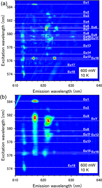
Figure A·4. CEES mappings of (a) ZnO:Eu/sapphire substrates and (b) the p-GaN/Al2O3/ZnO:Eu/n-ZnO LED structure.
Download figure:
Standard image High-resolution imageAppendix E.: Temperature Dependence of Eu Luminescence Doped in ZnO:Eu
Rare-Earth ions, including Eu3+ ions, are characterized by partially-filled 4f shells, which are localized inside of completely filled 5 s and 5p shells. This localization shields the electrons in the 4 f shell from the surrounding environment. As a result, rare-Earth ions maintain their "atom-like" properties and exhibit sharp optical luminescence/absorption bands associated with radiative transitions within the 4 f manifold, which are virtually insensitive to surrounding environment including injection current and temperature. Figure A·5a shows the temperature dependence of the PL spectra in the vicinity of ∼613 nm from Eu3+ ions in the LEDs. The peak wavelength of the PL spectrum at 15 K is located at 613.2 nm, exhibiting the gradual redshift with increasing measurement temperature. The peak wavelength becomes 613.7 nm at 300 K, corresponding to the average shift of the peak wavelength of <0.002 nm K−1. Figure A·5b shows the temperature dependence of the peak intensity of Eu luminescence at ∼613 nm whose spectra are shown in Fig. A·5a. All PL intensities are normalized by those measured at 15 K. The PL intensity shows gradual decrease with increased temperature, and the normalized PL intensity is almost 0.2 at 300 K.

Figure A·5. Temperature dependence of (a) the PL spectra and (b) their peak intensities in the vicinity of 613 nm from Eu luminescence in the p-GaN/Al2O3/ZnO:Eu/n-ZnO LED structure.
Download figure:
Standard image High-resolution image