

Abstract
In this paper, the electrical and ultraviolet optoelectronic properties of the interdigitated finger geometry β-Ga2O3 photodetector were investigated from the temperature of 40 K to 300 K. Under different light illumination conditions, when the temperature increased from 40 K to 300 K, the maximum current of the β-Ga2O3 photodetector was obtained around 180 K, which is related to the carrier mobility of β-Ga2O3. Under 365-nm illumination, when the temperature increased from 40 K to 300 K, the photo-to-dark current ratio (PDCR) of the β-Ga2O3 photodetector increased by 924%. Under 254-nm illumination, the PDCR decreased by 87%. Besides, the temperature point corresponding to the photoresponse peak under 365-nm illumination moved to the right under 254-nm illumination, indicating that the photodetector had a redshift at low temperature. Moreover, the fast photoresponse time under 365-nm and 254-nm illumination decreased when the temperature increased. This indicated that the defect concentration of Ga2O3 decreased gradually as the temperature increased, leading to the faster response time of the photodetector.
Export citation and abstract BibTeX RIS
There is no solar irradiation between 200 nm and 280 nm on the Earth's surface, which is called the solar blind zone because the stratospheric ozone absorbs deep ultraviolet (UV) light. 1,2 As a result, solar-blind photodetectors operating in the region can accurately detect very weak signals in the Sun and artificial lighting because of their black background. 3
Solar-blind photodetectors have been used in many civil and military applications, including fire detection, missile warning, non-line-of-sight optical communication, chemical/biological analysis, and UV astronomy. 4,5 Conventional deep-UV photodetectors based on Si- and GaAs are not truly solar blind and require additional visible-light blocking filters. 6 ZnO wurtzite and MgO rock salt have a maximum bandgap of 4.3 eV, which is not large enough for a solar-blind photodetector. Diamond, AlN, and cubic BN have very large band gaps of 5.5, 6.1, and 6.3 eV respectively, but they have limited detection capability for wavelengths shorter than 225, 210, and 193 nm. β-Ga2O3 is particularly suitable for solar-blind photodetector because of its bandgap of ∼4.5 eV. 7
Although solar-blind photodetectors made of β-Ga2O3 have great benefits in terms of response speed and stability, there are not many studies on the photoelectric characteristics and mechanisms of β-Ga2O3 photodetectors changing with temperature. The electrical and thermal conductivity properties of β-Ga2O3 have been extensively studied. 8 As the temperature increases, the number of thermally activated electrons will increase, affecting the device properties of β-Ga2O3. 9 In fact, at a high temperature, the mobility in Ga2O3 is limited by optical phonon scattering. At a low temperature, the mobility is limited by ionized impurity scattering. 10,11 In deep-space environments, temperatures can decrease as low as 133 K on Mars 12 and as low as 53 K on Jupiter. 13
In this letter, a β-Ga2O3 photodetector was prepared, and the structure, electrical, and photoelectric properties were characterized to study the effects of temperature on the photodetector of β-Ga2O3 at a temperature of 40–300 K.
Experiment
Firstly, Laser Molecular Beam Epitaxy (LMBE) was used to grow the β-Ga2O3 thin film on Al2O3 (0001) substrates. The base pressure in growing the chamber was 1×10⁻⁶ Pa. To explore the optimum growth condition, the growth temperature ranged from 650 °C to 850 °C and oxygen pressure ranged from 5×10⁻³ Pa to 5×10⁻¹ Pa. Then, the laser ablation was conducted at a laser fluence of 5 J cm−2 with a repetition target rate of 2 Hz using a KrF excimer laser with a wavelength of 248 nm. To improve the film uniformity, the substrate was rotated during deposition, and the distance between the target and substrate was 5 cm. Through a scanning electron microscope (SEM), the growing rate of 0.28 Å/pulse could be observed. The thickness of the films was estimated to be about 200 nm. The β-Ga2O3 thin film was undoped. Subsequently, to fabricate a photodetector, using a shadow mask by radio frequency magnetron sputtering, an interdigital Ti/Au electrode was deposited on the film, and then it was thermally annealed at 300 °C for 10 min in the Ar atmosphere. The electrode fingers have a width of 100 μm, a length of 2800 μm, and a spacing gap of 100 μm. The schematic diagram of the interdigital electrodes of the photodetector is illustrated in Fig. 1.
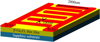
Figure 1. The schematic diagram of fabricated β-Ga2O3 solar-blind photodetectors.
Download figure:
Standard image High-resolution imageFigure 2 shows the XRD patterns of Ga2O3 thin films. The results indicate that all peaks are indexed as β-Ga2O3 (−201) and higher-order diffractions except for the substrate diffraction peaks. No other peaks apart from these are found, indicating a single (−201) plane orientation growth. Our previous work has investigated the impact of the electron beam on β-Ga2O3, and the results indicated that electron irradiation excites electron-hole pairs in β-Ga2O3 and increases traps in β-Ga2O3. 12
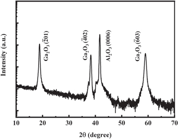
Figure 2. XRD patterns of Ga2O3 thin films.
Download figure:
Standard image High-resolution imageThen, temperature-dependent experiments were conducted on β-Ga2O3 photodetectors. The typical temperature points were selected at 40 K, 100 K, 160 K, 220 K, 280 K, and 300 K. The voltammetry curves and photo response curves of β-Ga2O3 photodetectors were measured by Keithley 4200 at different temperature points. The photoresponse curve was obtained by measuring the current of the β-Ga2O3 photodetector as time changed under a switching interval of 50 s and a bias voltage of 10 V. The timer used in the experiment is GCI-73 multifunctional precision electronic timer, which can ensure the accuracy of the switching interval. The light source was generated by ENF-240C, which is manufactured by the American Spectronics company. The light intensity of the 254-nm illumination and 365-nm illumination was 310 μw cm−2 and 300 μw cm−2 at a position of about 6 inches, respectively.
Results and Discussion
The experimental results of the β-Ga2O3 photodetector are shown in Fig. 3. Specifically, Figs. 3a, 3c, and 3e respectively show the I–V characteristics curve of the β-Ga2O3 photodetector in a dark condition, under 365-nm light illumination, and under 254-nm light illumination. The step of temperature is 60 K. Figures 3b, 3d, and 3f show the current change corresponding to each temperature point under a bias voltage of 10 V in a dark condition, under 365-nm light illumination, and under 254-nm light illumination. The step of temperature is 20 K. It can be seen from Fig. 3 that as the temperature increased from 40 K to 300 K, the current of the β-Ga2O3 photodetector rose first and then fell. At the voltage of 10 V, the β-Ga2O3 photodetector had the maximum current at the temperature of 160 K under the dark condition and 365-nm light illumination. However, at the voltage of 10 V, the β-Ga2O3 photodetector had the maximum current at the temperature of 220 K under 254-nm light illumination. To find the turning point at which the current changes with temperature, the step of the temperature was adjusted from 60 K to 20 K. The current of the β-Ga2O3 photodetector at the voltage of 10 V was then measured at different temperatures under different light conditions. The results are shown in the Figs. 3b, 3d and 3f. It can be seen that the transfer selection point of the current of the β-Ga2O3 photodetector with the change of temperature is around 180 K under the three light conditions.
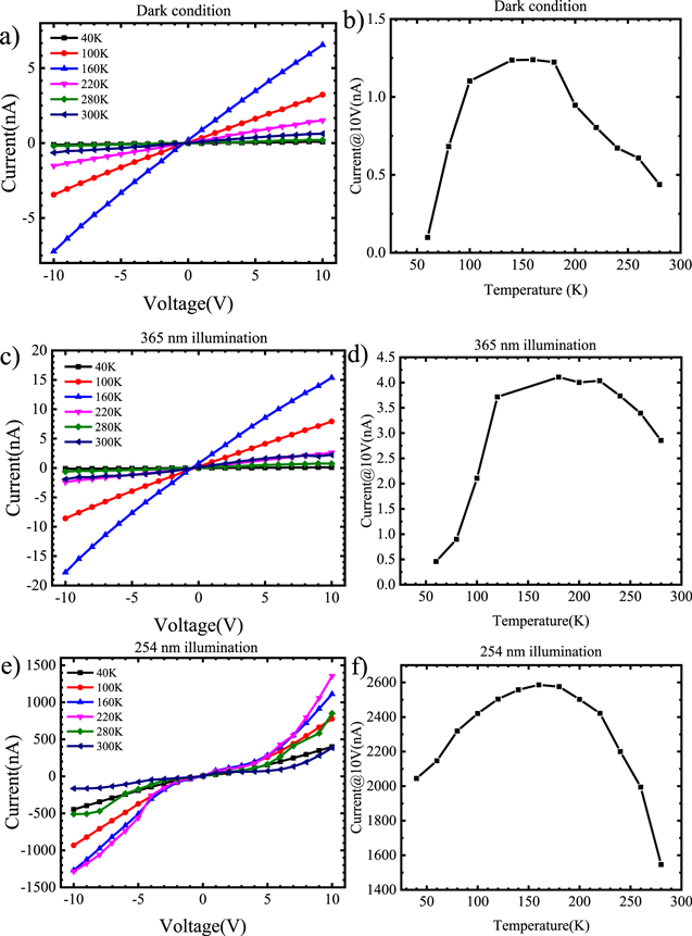
Figure 3. (a), (c), and (e) respectively show the I-V characteristics curve of the β- Ga2O3 photodetector in the dark condition, under 365-nm light illumination, and under 254-nm light illumination. The step of temperature is 60 K. (b), (d), and (f) respectively show the current change corresponding to each temperature point under a bias voltage of 10 V in the dark condition, under 365-nm light illumination, and under 254-nm light illumination. The step of temperature is 20 K.
Download figure:
Standard image High-resolution imageThe conductivity of n-type doped β-Ga2O3 can be expressed as  14
where n represents the electron concentration, q represents the unit charge, and μ represents the carrier mobility. Among the three variables, only μ is strongly correlated with temperature. It has been shown that the electron mobility in Ga2O3 reaches its maximum value around 190 K,
13
which explains why the turning point is around 180 K when the photocurrent changes with temperature.
14
where n represents the electron concentration, q represents the unit charge, and μ represents the carrier mobility. Among the three variables, only μ is strongly correlated with temperature. It has been shown that the electron mobility in Ga2O3 reaches its maximum value around 190 K,
13
which explains why the turning point is around 180 K when the photocurrent changes with temperature.
In addition to the current, photodetectors also have two very important parameters, namely photo-to-dark current ratio (PDCR) and photoresponse. PDCR represents the increase of the photocurrent relative to the dark current, and it is calculated as follows:

where IPhoto is the photocurrent of the β-Ga2O3 photodetector, and IDark is the dark current of the β-Ga2O3 photodetector. 15
Photoresponse represents the ratio of the photodetector's input signal to its output signal, and the calculation formula of photoresponse is

where Ad is the detective area, and Pd is the intensity of the UV light source. 16
In this study, the photo-to-dark current ratio and photoresponse of the β-Ga2O3 photodetector were calculated under different lighting conditions and different temperatures. The results are shown in Fig. 4.
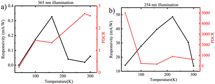
Figure 4. PDCR and photoresponse of the β-Ga2O3 photodetector for different temperatures under 365-nm illumination (a) and under 254-nm illumination (b).
Download figure:
Standard image High-resolution imageAs shown in Fig. 4, the PDCR and photoresponse under 254-nm illumination are much larger than those under 365-nm illumination. Meanwhile, the photoresponse of the β-Ga2O3 photodetector reached a peak both under 365-nm illumination and under 254-nm illumination, but the peak of the photoresponse of the β-Ga2O3 photodetector varied with the temperature. Under 365-nm illumination, the peak point was at 160 K, which was lower than that under 254-nm illumination. This may be related to the redshift phenomenon of photodetectors at low temperature, 17 indicating that the wavelength sensitive to the β-Ga2O3 photodetector may become longer under a low temperature. With the increase in temperature, the PDCR of the β-Ga2O3 photodetector increased gradually under 365-nm illumination but decreased gradually under 254-nm illumination. This indicated that as the temperature increased, the photocurrent generated by 365-nm illumination gradually increased while that generated by 254-nm illumination gradually decreased. Experimental results have shown that point defects, including oxygen vacancy VO, gap oxygen atom, gallium vacancy VGa and gap atom can be used as capture and recombination centers to reduce the collection efficiency of electric aurora carriers. Therefore, degradation of PDCR was caused. 18,19 Combined with the changes in the photo-to-dark current ratio under different lighting conditions, the reason that the photo-to-dark current ratio at 254-nm light illumination decreased with the increase of temperature was that the point defects increased with the temperature.
The temperature-dependent current-time (I–T) response of the β-Ga2O3 photodetector at 10 V under different UV light illumination conditions is shown in Fig. 5. The response-time characteristics of the β–Ga2O3 photodetectors at a temperature of 40 K–300 K by on/off switching under an applied bias of 10 V and under 365-nm and 254-nm light illumination are represented in Fig. 5. It can be observed that temperature has a considerable impact under different UV light illumination conditions. With the change of temperature, the response time and current of the photo will change correspondingly
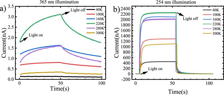
Figure 5. Response-time characteristics of the β-Ga2O3 photodetectors at a temperature of 40 K-300 K under 365-nm illumination (a) and 254-nm illumination (b).
Download figure:
Standard image High-resolution imageFor a more detailed comparative study of response times, quantitative analysis of the current rise and decay process involves the following biexponential relaxation equation to fit the photoresponse curve. 20

where I0
is the steady-state photocurrent; t is the time; C and D are the constant;  and
and  are two relaxation time constants. This equation indicates that there are two different components in the current rise and decay processes, and the magnitude of C and D means the proportion of each component. The time corresponding to a larger C and D is taken as the rise time and fall time of the β-Ga2O3 photodetector. Two time constants indicate that two different mechanisms are functioning during the current rise and decay process, which has been reported in many studies.
21
The first one is a fast band-to-band recombination mechanism in the bulk. It has a smaller time constant, and it can be used to measure the light response speed of the detector. The second one is attributed to the presence of surface states in the device. The surface states act as traps that slow down the response of the detector to the light pulse. This mechanism has a much larger time constant.
22
The rise and decay process of the β-Ga2O3 photodetector's photoresponse under different illumination conditions are fitted with formula 3. The smaller time constant in the rising process is denoted as
are two relaxation time constants. This equation indicates that there are two different components in the current rise and decay processes, and the magnitude of C and D means the proportion of each component. The time corresponding to a larger C and D is taken as the rise time and fall time of the β-Ga2O3 photodetector. Two time constants indicate that two different mechanisms are functioning during the current rise and decay process, which has been reported in many studies.
21
The first one is a fast band-to-band recombination mechanism in the bulk. It has a smaller time constant, and it can be used to measure the light response speed of the detector. The second one is attributed to the presence of surface states in the device. The surface states act as traps that slow down the response of the detector to the light pulse. This mechanism has a much larger time constant.
22
The rise and decay process of the β-Ga2O3 photodetector's photoresponse under different illumination conditions are fitted with formula 3. The smaller time constant in the rising process is denoted as  and the smaller time constant in the decay process is denoted as
  Then, the rise time and fall time of each temperature point were fitted by the first-order linear function, and the results are shown in Fig. 6.
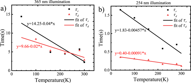
Figure 6. The fast response time of the β-Ga2O3 photodetector under 365-nm illumination (a) and 254-nm illumination (b) and the change of the first-order fitting curve with temperature.
Download figure:
Standard image High-resolution imageIt can see from Fig. 6 that the slopes of the first-order linear fitting curves are all negative, indicating that the photoresponse time of the β-Ga2O3 photodetector decreases with the increase of temperature, no matter under 365-nm or 254-nm illumination, indicating that the higher the temperature, the faster the photoresponse rate. To further analyze the reason why the fast response time of the β-Ga2O3 photodetector decreased with the increase in temperature, the photoluminescence (PL) was exploited under the temperature from 40 K to 300 K.
The excitation photo of 365-nm and 254-nm illumination was used to irradiate the β-Ga2O3, and the PL spectrum form is shown in Fig. 7. As the temperature increased, the PL intensity of both excitation photos decreased significantly. PL intensity refers to the number of photons emitted by the device at the corresponding energy. A higher PL intensity indicates that more photons are excited by the corresponding energy and there will be fewer defects. Therefore, the result in Fig. 7 shows that the number of defects in the β-Ga2O3 photodetector increased with the temperature.
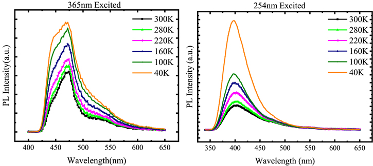
Figure 7. The PL spectra of the β-Ga2O3 photodetector at different testing temperatures by the exciting photo of 365 -nm (a) and 254-nm (b).
Download figure:
Standard image High-resolution imageTo determine which defect in β-Ga2O3 changes with temperature, this study adopted the Alentsev-FOCK method 23 to deconvolute the PL spectra shown in Fig. 7, and two representative temperature points of 40 K and 300 K were selected. The result is shown in Fig. 8. Under 365-nm excitation, the PL spectra were deconvoluted into three PL bands. At room temperature, the PL bands were centered at around 466 nm (∼2.64 eV), 527 nm (∼2.34 eV), and 570 nm (2.16 eV) (Fig. 8a). At the temperature of 40 K, the PL bands were centered at around 441 nm (∼2.79 eV), 467 nm (∼2.64 eV), and 511 nm (2.41 eV) (Fig. 8b). Under 254-nm excitation, the PL bands were centered at around 399 nm (∼3.09 eV), 438 nm (∼2.82 eV), and 534 nm (2.31 eV) (Fig. 8c) at room temperature. At the temperature of 40 K, the PL bands were centered at around 395 nm (∼3.12 eV) and 427 nm (∼2.89 eV) (Fig. 8d).
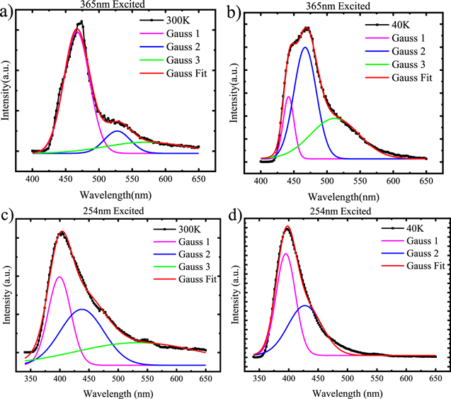
Figure 8. Deconvoluted PL spectra of β-Ga2O3 by the Alentsev-Fock method. An excitation wavelength of 254 nm at room temperature (a), at the temperature of 40 K (b). An excitation wavelength of 365 nm at room temperature c), at the temperature of 40 K (d).
Download figure:
Standard image High-resolution imageIn fact, the meaning of the deconvoluted PL bands is considered to be related to the recombination of a bound exciton with the hole trapped at one of the defects in β-Ga2O3 24 Specifically, the band peaking at around 3.0 eV is ascribed to (VGa+VO) disvacancies in the (1−) charge state, whereas the 2.7 eV PL emission correlates well with VGa with (2−) charge state. Similarly, the 2.4 eV PL emission is attributed to neutral oxygen interstitial (Oi 0) defects. 25 Therefore, under 365-nm excitation, the defect was VGa 2− at the temperature of 40 K. When the temperature increased gradually, the defect of Oi 0 occurred. Under 254-nm excitation, the defects were VGa 2− and (VGa+VO)1− at the temperature of 40 K. The defect of Oi 0 occurred when the temperature increased.
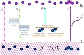
The generation and recombination mechanism of photo-generated carriers of the photodetector is shown in Fig. 9, which mainly involves the following four processes. Process 1: Under UV excitation, electron-hole pairs go directly from the valence band to the conduction band. Process 2: electron-hole pairs go to the defect-conduction band and then go to the conduction band. Process 3: with the illumination off, the electrons created in the conduction band recombine with the holes through the recombination centers. Process 4: the electrons go directly to the valence band to recombine with the holes. Under 254-nm UV illumination, photo-generated carriers are mainly from process 1 and only a few from process 2. However, under 365-nm UV illumination, photo-generated carriers are only from process 2. This is why the PDCR at 254-nm UV illumination is much larger than the PDCR at 365-nm UV illumination. The influence of temperature on the β-Ga2O3 detector is mainly in process 2. As the temperature increased, the defects of Oi 0 increased, indicating that the number of indirect transitions would increase. This explains why the photoresponse time becomes shorter under 365-nm illumination. Since the direct transition process also includes a small part of process 2. The photoresponse time also becomes shorter under 254-nm illumination, and the variation magnitude is much smaller than that in the indirect transition. This can be seen from the fact that the slope of Fig. 6a is much larger than that of Fig. 6b.
Figure 9. Schematic diagram illustrating the carrier transport mechanisms in the β-Ga2O3 photodetector.
Download figure:
Standard image High-resolution image
Conclusions
This paper conducted experiments to investigate the temperature-dependent properties of the β-Ga2O3 photodetector. The temperature of the experiment is from 40 K to 300 K. Under different light illumination conditions, when the temperature increased from 40 K to 300 K, the maximum current of the β-Ga2O3 photodetector was obtained at around 180 K, which is related to the carrier mobility of β-Ga2O3. Under 365-nm illumination, the photo-to-dark current ratio (PDCR) of the β-Ga2O3 photodetector increased from 0.25 to 2.56 when the temperature increased from 40 K to 300 K, and the photoresponse peak was at 160 K. Under 254-nm illumination, the PDCR of the photodetector decreased from 4986.63 to 609.29 when the temperature increased from 40 K to 300 K, and the photoresponse peak was at 220 K. These results indicated that as the temperature increased, the release of impurities or traps in the bandgap led to an increase in the number of photo carriers generated under 365-nm illumination and a corresponding decrease in the number of photo carriers generated under 254-nm illumination. The change of the photoresponse peak indicated that the photodetector had a redshift at low temperatures. Meanwhile, the fast photoresponse time under 365-nm and 254-nm illumination decreased as the temperature increased. This indicated that the defect concentration of Ga2O3 increased gradually with the temperature, leading to a faster response time of the photodetector. Our research provides a theoretical basis for the application of β-Ga2O3 photodetectors in the space environment in the future.
Acknowledgments
This work was supported by the National Natural Science Foundation of China (Grant Nos. 12075069, 61771167, 11775061, and 11805045), the key project of Science and Technology of Sichuan Province (Grant No. 2019YFSY0028), and the project of State Key Laboratory of Intense Pulsed Radiation Simulation and Effect (Grant Nos. SKLIPR1912and SKLIPR2015).