
Abstract
The surface condition under the gate is critically important to improve the device characteristics and thus reliability of the AlGaN/GaN high electron mobility transistor (HEMT). In this report, we demonstrated the reduction of leakage current (IG) with betterment of current collapse in Al0.25Ga0.75N/GaN Schottky gate (SG)-HEMT by improving metal/GaN interface using optimized ultraviolet-ozone (UV/O3) plasma treatment with post metal annealing modulation at 450 °C. The x-ray photoelectron spectroscopy (XPS) was used to verify the formation of GaOXNY layer at the metal/GaN interface. Owing to, the screening of the internal/external polarization charges by 10 min. UV/O3 surface plasma treatment and incremental increase of Schottky barrier height (ΦB) with post metal annealing modulation, resulted in the positive shifting of threshold voltage (VTH) in SG-HEMT. Due to the combined effects of the UV/O3 plasma treatment and metal annealing modulation, the magnitude of the interface trap density were effectively reduced to one order of magnitude, which further improved the current collapse significantly in SG-HEMT to 2.5% from 12.2%. The 10 min. UV/O3 treated SG-HEMT with PMA modulation exhibited decent performance with an IDMAX of 620 mA mm−1, a GMMAX of 135 mS mm−1, a threshold voltage (VTH) of −1.8 V, a higher ION/IOFF ratio of approximately  a subthreshold swing (SS) of 83 mV dec−1, with a low gate leakage current of
Export citation and abstract BibTeX RIS

This is an open access article distributed under the terms of the Creative Commons Attribution 4.0 License (CC BY, http://creativecommons.org/licenses/by/4.0/), which permits unrestricted reuse of the work in any medium, provided the original work is properly cited.
Corrections were made to this article on 17 06 2022. Author names and correspondence information were corrected.
The AlGaN/GaN-based power devices are emerging as potential candidate for the next generation power switching and high frequency applications due to their unique features such as, wide band gap (∼3.4 eV), high breakdown field (> 3 MV cm−1), and large saturation velocity (∼ cm s−1).
1–5
The polarization induced high density two dimensional electron gas (2DEG) generated at the AlGaN/GaN heterojunction enables the high electron mobility transistors (HEMTs) to function with low ON-resistance under normally ON condition.
5
cm s−1).
1–5
The polarization induced high density two dimensional electron gas (2DEG) generated at the AlGaN/GaN heterojunction enables the high electron mobility transistors (HEMTs) to function with low ON-resistance under normally ON condition.
5
In addition to the high voltage, high speed, and low on resistance characteristics of the AlGaN/GaN HEMTs, the high gate leakage current (IG) affects noise, reliability and radio-frequency power loss of the device. 6 Thus, the gate leakage current should be carefully examined. The high gate leakage current due to the strong polarization-induced electric field and Schottky gate contact limits the performance of the AlGaN/GaN HEMTs. 7 Moreover, Cl2-based inductively coupled plasma (ICP) dry etching system, correspondingly induces trap states in a device, leading to severe gate leakage current. 8
The gate leakage current is highly dependent on the surface condition and surface treatment methods used to reduce the interface trap densities rather than the intrinsic parameters. 6 Previous reports also mention that the carrier charging/discharging at a large amount of traps could results in degradation in conduction current, dynamic on-resistance, current collapse, switching loss and induce trap assisted tunneling etc during device operation. 9–13
Moreover, observations also confirm that due to the presence of lots of surface states at source/drain (S/D) access region, the HEMTs suffer from severe current collapse. 14 Numerous methods were introduced to improve the surface and interface states, such as dry etching, 15 wet cleaning, 15 interface passivation layers 16 and surface plasma treatment. 17–19
Among different surface treatment, the ultraviolet/ozone (UV/O3) surface plasma treatment is useful to reduce the gate leakage current as well as improves the surface traps. 6 Previous reports mentioned, for GaN-based electronic devices the Gallium-oxide (Ga–O) layer is of attention as a surface dielectric layer. 20 The ultraviolet/ozone surface plasma treatment could screen the effect of polarization charges by forming the GaOXNY layer on the GaN surface. 21 Moreover, the thin GaOXNY layer serves as passivation layer, which effectively reduce the surface traps. Previous reports also mentioned that the post metal annealing (PMA) modulation could significantly improves the Schottky barrier height (ΦB), which subsequently reduce the gate leakage current as well as shifts the VTH towards positive direction. 22 To date, the direct observation in the positive shifting of VTH with significant reduction of gate leakage current in optimized UV/O3 treated Schottky gate (SG)-HEMT with PMA modulation has not yet been investigated.
With this aim in mind, in this work, the interface of the SG-HEMTs was improved through optimized UV/O3 surface plasma treatment and post metal annealing modulation. Dramatic reduction of the current collapse and gate leakage current in the 10 min. UV/O3 treated SG-HEMT was observed. The UV/O3 treatment is a multi-functional process, which could screen the internal/external polarization charges, which resulted positive shifting the VTH in SG-HEMT compared to conventional HEMT. In addition, the metal annealing treatment significantly improved the ΦB, which further shifts the VTH towards positive. The 10 min. UV/O3 treated SG-HEMT with PMA modulation exhibited decent performance with an IDMAX of 620 mA mm−1, a GMMAX of 135 mS mm−1, a threshold voltage (VTH) of −1.8 V, a higher ION/IOFF ratio of approximately  a subthreshold swing (SS) of 83 mV dec−1, with a low gate leakage current of
Experimental
The AlGaN/GaN heterostructure was grown on Si substrate by metal organic chemical vapour deposition (MOCVD) system. The heterostructure consisted with 3.9 μm GaN buffer layer, a 300 nm undoped GaN layer, a 20 nm Al0.25Ga0.75N barrier layer, and a 2 nm GaN cap layer. The mobility and sheet carrier concentration were found to 2338 cm2 V−1. s and 6.15  1012 cm−2, respectively. The sheet resistance (Rsh) and contact resistance (Rc) were found to be approximately 400 Ω ϒ−1 and (1 ∼ 1.2) Ω.mm, respectively. After mesa isolation by inductive coupled plasma reactive ion etching (ICP-RIE) system, the source and drain regions were defined by UV-photolithography and Ti/Al/Ni/Au (25/150/30/120 nm) were deposited by electron beam evaporator. After that, the rapid thermal annealing (RTA) was done at 875 °C for 30 s. After that to create an O-rich interlayer between gate dielectric and GaN cap layer UV–Ozone surface plasma treatment was done with 7 mg l−1 O3 dose and active wavelengths of 185 nm and 254 nm for 10 min, prior to gate oxide deposition. Finally, the Schottky gate area was defined and Ni/Au (80/100 nm) metal stacks was deposited. Furthermore, to improve the device performance a post metal annealing (PMA) treatment was carried out at 450 °C for 5 min. Moreover, to optimize the UV/O3 surface treatment, another device was fabricated with 4 min. UV/O3 treatment prior to gate deposition. In addition, as a reference device, another two conventional HEMT were fabricated following the same protocol, (i) without UV/O3 and PMA treatment, and, (ii) without UV/O3 and with PMA treatment. The gate lengths (LG), and gate width (WG) for all devices were 2 μm and 100 μm, while gate to drain distance (LGD) and gate to source distance (LSG) were approximately to be 2 μm. Figures 1a and 1b show the schematic diagram of the SG-HEMT before and after UV/O3 treatment and PMA modulation.
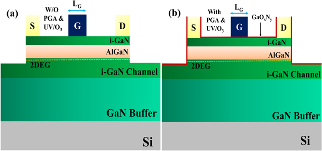
Figure 1. Schematic cross-section of the SG-HEMT (a) without UV/O3 treatment and PMA modulation and (b) with UV/O3 treatment and PMA modulation.
Download figure:
Standard image High-resolution imageResults and Discussion
Figures 2a and 2b show the typical atomic force microscopy (AFM) image of the conventional HEMT with and without surface treatment. It was found that the surface roughness was reduced form 0.72 nm to 0.29 nm after 10 min. UV/O3 plasma treatment as shown in Fig. 2c. The AFM image of the 10 min. UV/O3 plasma treated SG-HEMT with PMA modulation is shown in Fig. 2d. The combined process of the UV/O3 surface treatment with metal annealing, further reduce the surface roughness value to 0.26 nm. The dual treatment reduced the surface roughness to a great extent which subsequently improves the device performance.
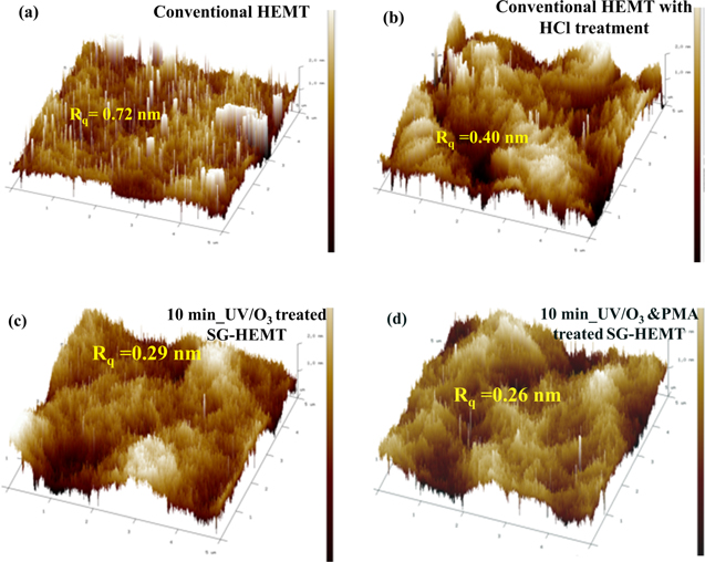
Figure 2. AFM images of the conventional HEMT (a) w/o & (b) with surface treatment and 10 min. UV/O3 treated SG-HEMT (c) w/o PMA modulation and (d) with PMA modulation.
Download figure:
Standard image High-resolution imageTo analysis the effect of UV/O3 surface treatment on the SG-HEMT device performance, the x-ray photoelectron spectroscopy (XPS) was adopted by using k-alpha x-ray photoelectron spectrometer. Figures 3a–3c exhibits the change in atomic composition in Ga 3d core levels before and after UV/O3 surface treatment, where both spectra were deconvoluted into two peaks of Ga–N and Ga–O. The Ga 3d5/2 peak and Ga2O3 (Ga3+) peak was de-convoluted by considering spin-orbital splitting. 21 It is obvious from Fig. 3c that the intensity of the Ga–O is much higher after 10 min. UV/O3 surface treatment. The peak intensity ratio of the Ga–O/Ga–N was significantly improved to 30% from 7%. Since the Gibbs free energy of the Ga–O bond is negatively larger (−285 kJ mol−1) than Ga–N bond (−157 kJ mol−1), the Ga atoms in the Ga–O bond could come from the Ga–N bond. 21
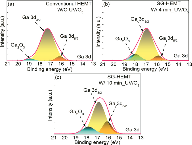
Figure 3. XPS images of the (a) conventional HEMT, (b) with 4 min and (c) 10 min. UV/O3 treated SG-HEMT.
Download figure:
Standard image High-resolution imageThe typical drain current-voltage characteristics (ID-VD) of the conventional HEMT and SG-HEMT with and without PMA modulation is shown in Figs. 4a and 4b. The maximum drain current of the 10 min. UV/O3 treated PMA modulated SG-HEMT was 620 mA mm−1 (@ VG = 3 V), while for 4 min. UV/O3 treated SG-HEMT the IDMAX was found to be 507 mA mm−1 (@ VG = 1 V). For comparison, IDMAXs were measured for the conventional HEMT without UV/O3 treatment before and after gate annealing modulation. The IDMAXs were found to be 510 mA mm−1 and 521 mA mm−1 before and after PMA. Owing to, large gate leakage currents the conventional HEMT could not biased with high VG. Henceforth, the reduction of IDMAX in conventional HEMT was attributed to the large gate leakage current. 23 In addition, with that due to combined treatment a significant reduction of ON-resistance (RON) was found in PMA modulated UV/O3 treated device than conventional HEMT to 5.6 Ω mm from 7.5 Ω mm.
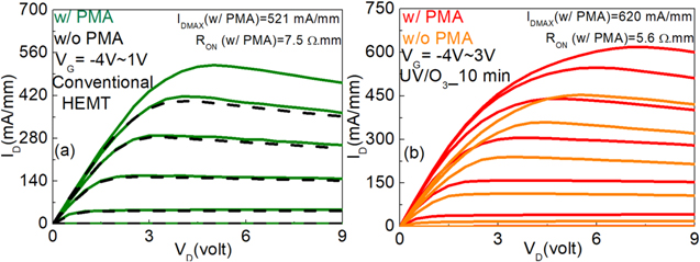
Figure 4. ID-VD characteristics of the (a) conventional HEMT and (b) 10 min UV/O3 treated SG-HEMT before and after PMA modulation.
Download figure:
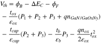
Standard image High-resolution imageTo understand the gate controllability of the SG-HEMT after UV/O3 treatment with PMA modification the transfer characteristics (@ VD = 6 V) was calibrated and compared with reference devices as shown in Fig. 5. The threshold voltage was defined as the gate bias intercept point of the linear extrapolation of the ID at maximum transconductance. 24 The VTH's of the 10 min. and 4 min. UV/O3 treated SG-HEMT were found to be approximately −3 V and −3.5 V, respectively as shown in Fig. 5. The VTH was found −3.52 V for conventional HEMT. Previous studies reported, the negative shifting of VTH in metal oxide semiconductor (MOS)-HEMT compared to conventional HEMT. 25 Owing to the band bending at metal/GaN interface causing the UV–ozone treatment, results the positive shifting of VTH in UV/O3 treated SG-HEMT compared to conventional HEMT. 3,6,26 After PMA treatment at 450 °C the threshold voltage was further shifted towards positive direction and found to be approximately −1.8 V. The threshold voltage can be expressed as: 27
Where,  is the metal barrier height,
  is the energy difference EC
-EF
(EF
is the Fermi energy) in the GaN bulk,
is the energy difference EC
-EF
(EF
is the Fermi energy) in the GaN bulk,  is the conduction band offset between,
  is the barrier thickness,
  is the GaOXNY thickness,
  is the permittivity of the barrier layer,
  is the permittivity of the oxide layer,
  is the oxide charge,
  is the interface charge density at the SiO2/GaOXNY interface,
  are the total polarization sheet charges (sum of the spontaneous and piezoelectric polarization) at the GaN-cap surface, GaN-cap/AlGaN interface, and AlGaN/GaN buffer interface, respectively. Owing to, the screening of the internal/external polarization charges by forming GaOXNY layer causing the UV/O3 treatment, resulted in the VTH shifts towards positive direction after 10 min. UV/O3 surface treatment.
6
Furthermore, from equation (1) it can be understood that, due to the incremental increase of the
are the total polarization sheet charges (sum of the spontaneous and piezoelectric polarization) at the GaN-cap surface, GaN-cap/AlGaN interface, and AlGaN/GaN buffer interface, respectively. Owing to, the screening of the internal/external polarization charges by forming GaOXNY layer causing the UV/O3 treatment, resulted in the VTH shifts towards positive direction after 10 min. UV/O3 surface treatment.
6
Furthermore, from equation (1) it can be understood that, due to the incremental increase of the  after gate annealing treatment the VTH shifts significantly towards positive direction.
22
There was no significant change in VTH was found for conventional HEMT after annealing treatment.
after gate annealing treatment the VTH shifts significantly towards positive direction.
22
There was no significant change in VTH was found for conventional HEMT after annealing treatment.
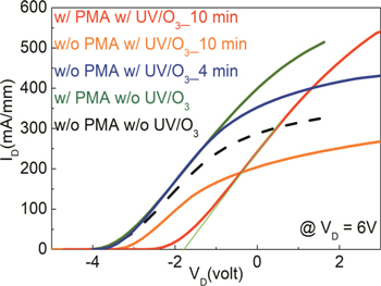
Figure 5. Transfer characteristics of all devices @ (VD = 6 V).
Download figure:
Standard image High-resolution imageTo understand the effect of combine treatment on the extrinsic transconductance of the different devices, the transfer characteristics were measured (@ VD = 6 V) for the UV/O3 treated SG-HEMT and conventional HEMT before and after PMA modulation as shown in Figs. 6a and 6b. The significant improvement of the peak extrinsic transconductance (GMMAX) was observed in the 10 min. UV/O3 treated SG-HEMT after metal gate annealing modulation compared to conventional HEMT. The GMMAX's were found to be approximately 135 mS mm−1 (91 mS mm−1) and 120 mS mm−1 (105 mS mm−1) in the 10 min. UV/O3 treated SG-HEMT and conventional HEMT with annealing (without annealing) modulation. In addition, to understand the linearity behaviour of the device the gate voltage swing (GVS), defined as the 10% drop of the maximum transconductance, were calculated for both devices. 25 The GVS improved to 1.62 V from 0.75 V in 10 min. UV/O3 treated SG-HEMT after metal gate annealing modulation. Thus, low phase noise, the device linearity, and wide dynamic range were improved after dual surface treatment and post gate modulation in stack layer MOS-HEMT. 25 Moreover, the GMMAX was found to be approximately 118 mS mm−1 for 5 min. UV/O3 treated device.
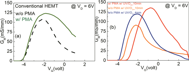
Figure 6. Transfer characteristics of the (a) conventional HEMT, and (b) 4 min and 10 min. UV/O3 treated SG-HEMT before and after PMA modulation.
Download figure:
Standard image High-resolution imageThe subthreshold characteristics (@ VD = 6 V) as a function of gate voltage, for all the devices is shown in Fig. 7. It was clearly found that the subthreshold drain leakage current decreased approximately two orders of magnitude in 10 min. UV/O3-treated SG-HEMT with PMA modification, compared to the conventional HEMT. The subthreshold drain leakage current is dominated by the reverse biased gate leakage current (IG) in the pinch-off region.
22
Since, the IG was suppressed in SG-HEMT after UV/O3 surface treatment and PMA modification, the subthreshold drain leakage current was decreased. The subthreshold swing (SS) was also highly dependent on the reverse biased gate leakage current.
22
To understand the gate controllability, the SS values of all the devices were calculated from Fig. 7. The UV/O3-plasma treated device exhibited much lower SS value after gate annealing treatment compared to conventional HEMT. The subthreshold swing values were found to be approximately 83 mV dec−1 (138 mV dec−1) and 180 mV dec−1 (195 mV dec−1) after PMA (before PMA) modification for 10 min. UV/O3 treated SG-HEMT and conventional HEMT, respectively. In addition, the ON/OFF ratio (ION/IOFF) was also increased significantly after dual surface treatment in SG-HEMT. ION/IOFF for 10 min. UV/O3 treated SG-HEMT and conventional HEMT with PMA (without PMA) were found to be approximately  (
( ) and
) and  respectively. The SS and ION/IOFF were found 125 mV dec−1 and
  respectively for 4 min. UV/O3 treated SG-HEMT.
Figure 7. Reverse gate leakage and subthreshold characteristics@ (VD = 6 V) of all devices.
Download figure:
Standard image High-resolution imageThe forward and reverse gate leakage I–V characteristics of all devices is shown in Fig. 7. The reversed gate leakage current was significantly reduced after UV/O3 and gate annealing modification. The off-state gate leakage current (@ VG = −12 V) of the 10 min. UV/O3 treated device after metal annealing was nearly ∼10−9 A mm−1, approximately three orders lower than of the reference devices. The reason for the improved subthreshold characteristics and off- state gate leakage current is mainly due to the reduction of interface trap density of the GaN MOS capacitor by the formation of GaOXNY interface passivation layer and the increased Schottky barrier height with improved surface quality through UV/O3 treatment
21
with PMA modification.
28
The effective Schottky barrier height (SBH) and ideality factor ( ) can be extracted by employing the standard thermionic equation.
29
The Schottky barrier height/ideality factor were found for conventional device and 10 min. UV/O3-treated SG- HEMT with PMA modulation 0.45 eV/3.2 and 1.4 eV/1.92, respectively.
) can be extracted by employing the standard thermionic equation.
29
The Schottky barrier height/ideality factor were found for conventional device and 10 min. UV/O3-treated SG- HEMT with PMA modulation 0.45 eV/3.2 and 1.4 eV/1.92, respectively.
To investigate the effectiveness of the optimized UV/O3 surface treatment and post metal annealing modulation in the SG-HEMT compared to conventional device, the gate lag measurements was employed. Figures 8a and 8b, show the drain current response of the 10 min. UV/O3 treated SG-HEMT with PMA modification and 4 min surface treated SG-HEMT. To understand the effect of metal annealing treatment separately, the gate lag measurements were also done for conventional HEMT before and after gate annealing treatment as shown in Figs. 8c and 8d. The pulse width and pulse period are set to 500 μs and 50 ms respectively. The observations clearly revealed that the current collapse was significantly improved in SG-HEMT with 10 min. UV/O3 treatment and PMA modification than conventional HEMT. The drain-source current collapse was significantly improved to 2.5% (10.1%) in 10 min. UV/O3 treated SG HEMT (conventional HEMT) after PMA modulation, while for 4 min. UV/O3 treated SG HEMT and conventional HEMT it was found approximately to be 7.2% and 12.2% (@ VD = 8 V, VG = 0 V). The most of the surface traps presented in the Source-Drain access regions might have been reduced by UV/O3 surface modification and post metal annealing treatment, which resulted the improvement in the current collapse significantly. Due to the formation of the thin Ga–O interface layer between gate metal and GaN cap, which serves as the passivation layer resulted in the reduction of current collapse in SG-HEMT. 21,30
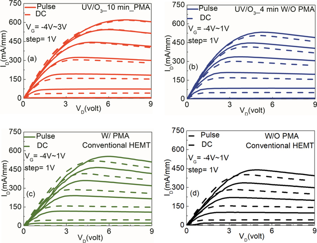
Figure 8. Comparison of pulsed ID-VD characteristics of the SG-HEMT (a) with 10 min UV/O3 treatment and PMA modulation, (b) with 4 min. UV/O3 treatment without PMA modulation, and conventional HEMT (c) with & (d) without PMA modulation.
Download figure:
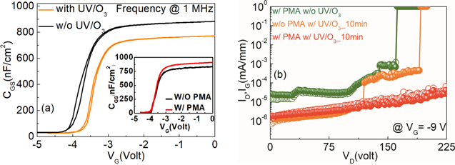
Standard image High-resolution imageIn order to understand the reduction of trap states in the optimized UV/O3 surface treated metal annealing modulated SG-HEMT and conventional HEMT, the capacitance-voltage (C-V) measurements for both devices were done at 1 MHz shown in Fig. 9a. The interface state density (Dit) for can be extracted from the previously reported formula.
31
The Dit's were estimated to be  for UV/O3 treated SG-HEMT (Conventional HEMT). The similar trend was found in the previous report.
32
Owing to the combined effects of the optimized UV/O3 surface treatment and post metal annealing modulation the interface trap density was significantly reduced about one order of magnitude in SG-HEMT. The post metal annealing process could reduce the interface state densities effectively. It is inferred that the trap states are mainly nitrogen vacancies. The decreased of trap states means the reduction of nitrogen vacancies by PMA process with N2 gas and due to diffusion of gate metal.
8,33
Moreover, previous studies also mentioned that the PMA could effectively reduce shallow traps by the creation of deep traps, which subsequently reduces the interface state density.
34
In addition, the C-V characteristics of the conventional HEMT with and without PMA treatment is shown in the inset of Fig. 9a.
for UV/O3 treated SG-HEMT (Conventional HEMT). The similar trend was found in the previous report.
32
Owing to the combined effects of the optimized UV/O3 surface treatment and post metal annealing modulation the interface trap density was significantly reduced about one order of magnitude in SG-HEMT. The post metal annealing process could reduce the interface state densities effectively. It is inferred that the trap states are mainly nitrogen vacancies. The decreased of trap states means the reduction of nitrogen vacancies by PMA process with N2 gas and due to diffusion of gate metal.
8,33
Moreover, previous studies also mentioned that the PMA could effectively reduce shallow traps by the creation of deep traps, which subsequently reduces the interface state density.
34
In addition, the C-V characteristics of the conventional HEMT with and without PMA treatment is shown in the inset of Fig. 9a.
Figure 9. Comparison of capacitance-voltage characteristics of the (a) with and without UV/O3 treated devices and PMA modulation (inset). Breakdown voltage of the (b) conventional HEMT and 10 min. UV/O3 treated SG-HEMT with and without PMA modulation.
Download figure:
Standard image High-resolution image
The three terminal off-state breakdown characteristics of different devices is shown in Fig. 9b. The breakdown voltages (VBR) were found to be 155 V, and 175 V for conventional HEMT with PMA treatment and 10 min. UV/O3 treated SG-HEMT, respectively. Whereas the VBR was significantly improved to >225 V for 10 min. UV/O3 treated SG-HEMT after annealing modulation. As discussed earlier, due to the dual surface treatment the gate/GaN interface was improved with greater dangling bond passivation. Moreover, after annealing treatment due to the reduction of shallow traps the IG was significantly decreased, which resulted in much higher VBR in UV/O3 treated SG-HEMT with PMA modulation compared to conventional HEMT device.
Conclusions
In summary, we have demonstrated the combined effects of optimized UV/O3 plasma treatment and post metal annealing modulation on the DC performance of AlGaN/GaN SG-HEMT. A 10 min. UV/O3 surface plasma treatment produced a thin interface layer of GaOXNY in between Ni/GaN interface, serves as the passivation layer in Schottky gate (SG)-HEMT. In addition, with GaOXNY layer the metal annealing treatment significantly reduced the current degradation from 12.2% to 2.5% by decreasing the trapping phenomenon originating from surface states. A significant enhancement of electrical characteristics in SG-HEMT were observed after the combined treatment compared to the conventional HEMT. The SG-HEMT with 10 min. UV/O3 surface plasma treatment after PMA exhibited IDMAX of 620 mA mm−1, GMMAX of 135 mS mm−1, on-off ratio of 1.2  with subthreshold slope of 83 mV dec−1 and VTH of − 1.8 V. The combined effects of band bending at the Ni/GaN interface and screening of internal/external polarization bound charges by the UV/O3 surface treatment shifted the VTH towards positive direction in SG-HEMT, compared to conventional HEMT. The reversed gate leakage current was approximately to be
  −9 A mm−1, were achieved. Owing to the incremental increase of Schottky barrier hight from 0.45 eV to 1.4 eV the IG was decreased more than two orders of magnitude after gate annealing modulation. Furthermore, the aforementioned combined treatment decreased the interface trap states from
 to
to 
 in 10 min. UV/O3 treated SG-HEMT after gate annealing treatment compared to conventional HEMT. The experimental results are important for the advancement of the high performance AlGaN/GaN-based SG-HEMT.
Acknowledgments
This research was funded by the Ministry of Science and Technology, Taiwan, grant numbers MOST 106-2221-E-006-219-MY3 and MOST 109-2221-E-06–075-MY2 and Transcom. Inc., Taiwan, grant number 109S0172. The authors also acknowledge the use of TEM, EDS, and ALD belonging to the Core facility center of National Cheng-Kung University.