
Abstract
The metastable cubic γ-(Ga1−xMnx)2O3 thin films are successfully obtained at high growth temperature by laser molecular beam epitaxy technology. The optoelectronic properties of the solar blind Schottky-type photodetectors (PDs) based on γ-(Ga1−xMnx)2O3 thin films are reported for the first time. In this experimental system, the γ-(Ga0.96Mn0.04)2O3 PD exhibits the highest light-to-dark ratio (LDR) of 6.89 × 10³, which is two orders of magnitude higher than the pure β-Ga2O3 PD prepared under the same condition. In addition, it shows a fast photoresponse decay speed of about 0.081 s. The results suggest that Mn element is expected to be one of the promising dopants to induce and stabilize the metastable γ-Ga2O3, as well as optimize the optoelectronic performance of photodetectors.
Export citation and abstract BibTeX RIS

This is an open access article distributed under the terms of the Creative Commons Attribution 4.0 License (CC BY, http://creativecommons.org/licenses/by/4.0/), which permits unrestricted reuse of the work in any medium, provided the original work is properly cited.
Ga2O3, an ultra-wide bandgap semiconductor, is a promising material for power electronics and ultraviolet photodetectors. Recently, Zeng et al. reported a Ga2O3 based field-plated metal oxide semiconductor field-effect transistor with a breakdown field of 4.4 MV cm−1.1 This ultra-high experimental data has surpassed the theoretical limitations of SiC (3.18 MV cm−1) and GaN (3 MV cm−1), verifying the application prospect of Ga2O3.2
Ga2O3 has five polymorphs, named α, β, γ, ε and δ. Among them, the β phase has the best thermal and chemical stability, even work with concentrated acids. Moreover, due to its superior properties such as large Baliga's figures of merit (over 3000) and low cost, β-Ga2O3 based materials and devices are under the highest enthusiasm of research.3 However, the monoclinic structure makes it difficult to improve the β-Ga2O3 epitaxial thin film quality on the mainstream substrate, as well as the intrinsic n-type conductivity also limits its development in power devices to some extent. Therefore, exploring the application potential in different fields of other metastable phases, as well as realizing phase controlled growth of high-quality epitaxial thin films, is a critical path for the further development of Ga2O3 materials. Compared with β-Ga2O3, the metastable γ phase may have more attractive physical properties and promising applications. For example, it has a defective spinel type structure containing cation vacancies in tetrahedral and octahedral sites, which makes it one of the best candidates for new-generation diluted magnetic semiconductors.4 In addition, among all of the polymorphs, γ-Ga2O3 has the largest surface area of the nanostructure, exhibiting high photocatalytic activity and light-emitting characteristics in the ultraviolet and blue light regions.5 Till now, some papers have substantiated its potential applications in ferromagnetic, photocatalytic, piezoelectric and photoluminescent devices.6–10 However, the optoelectronic property of γ-Ga2O3 has rarely been reported. To our best knowledge, only one scientific research team of Teng, Ruan and Wang et al. have thoroughly studied the functionality of γ-Ga2O3 PDs.11–13 They constructed several shapes of γ-Ga2O3 PDs and compared their performance, such as nanoflowers, nanospheres, microspheres and nanosheets. Among them, the nanosheets PD (thickness, 15 nm) exhibited the highest LDR of 1.64 × 10⁴ and the shortest response time of 0.06 s.
Although the PDs based on γ-Ga2O3 nanomaterials have good performance, the construction always requires complicated growth process,as well as the repeatability are often poor, which is not conducive to commercial application. Hence, the PDs based on γ-Ga2O3 thin films are under urgent need. Till now, several dopants have been attempted to stabilize the γ-Ga2O3 thin films, such as Cu,10 Mn6,14–16 and Si.17 However, these papers are mainly focus on the ferromagnetic, optical or photoluminescent properties of the films, and the optoelectronic detective characteristics are rarely been studied.
In this paper, Mn dopant is used to induce and stabilize the phase transition. Our group has verified that while doping Mn ions, the change of Mn valence from +3 to +2 could suppress the unintentional extra electrons, decrease dark current, enhance the LDR and speed up the response time of β-(GaMn)2O3 PD.18 Herein, the effect of Mn dopant on structural and optoelectronic properties of γ-Ga2O3 thin film PDs has been systematically analyzed.
Experimental
The (Ga1−xMnx)2O3 (x = 0, 0.02, 0.04, 0.06, 0.08) targets were prepared by a standard solid- state reaction method. High purity (5 N) powders were thoroughly mixed, ground, and annealed at 1073 K for 8 h in air atmosphere twice. And then pressed into a Φ 25 × 4 mm target size followed a sintering process at 1273 K for 8 h in air atmosphere. Subsequently, (Ga1−xMnx)2O3 thin films were grown on sapphire substrates by laser molecular beam epitaxy method at 1023 K. The laser energy was 400 mJ with the repetition rate of 2 Hz. The oxygen pressure was 2 × 10⁻³ Pa. The distance between target and substrate was 45 mm. After deposition, there followed an in situ annealing process at the same environment for 30 min.
The crystalline structure and orientation of the films were analyzed via Bruker D8 Discover X-ray diffraction (XRD) θ−2θ scans and pole figure measurements. And the surface morphology was characterized by a NOVA NanoSEM 450 scanning electron microscope (SEM). Ultraviolet-visible (UV–vis) absorption spectrum was taken using a Hitachi U-3900 UV–visible spectrophotometer. To measure the optoelectronic properties, an interdigital Ti/Au electrode was deposited on (Ga1−xMnx)2O3 thin film by magnetron sputtering method. A shadow mask was used as shown in Fig. 5. The electrode fingers were 200 μm wide and 3900 μm long with a 200 μm spacing gap. Hence the effective irradiated area was about 0.043 cm2. After deposition, there followed a post annealing process in air atmosphere at 573 K for 3 h for all PDs.
Results and Discussion
Figure 1 shows the XRD patterns of (Ga1−xMnx)2O3 powders, which have been ground and sintered by two times. After comparing with the standard PDF card given by the powder diffraction committee, it can be concluded that, when x ≤ 0.04 the XRD peaks of all the sintered products can match the diffraction peaks of β-Ga2O3 powder. However, when x > 0.04, the diffraction peaks of bixbyite structural Mn2O3 powder gradually appear [PDF#41–1442]. This indicates that phase separation arises when the doping concentration is high, and Ga2O3@Mn2O3 eutectic substance may appear in the powder. Figure 1b shows the enlarged diffraction peaks near 2θ = 18.9º. It can be seen that, after doping with Mn element, the diffraction peaks are slightly shift to smaller 2θ at first. However, with the further increase of doping concentration, especially when x = 0.06 and 0.08, the peaks gradually move to higher angle position. This may be due to the influence of Mn2O3 material or the lattice strain caused by the doping of Mn ions with various valence states. The Mn2+, Mn3+, Mn4+ and Ga3+ ionic radii are 0.83, 0.64, 0.53 and 0.62 Å, respectively.19
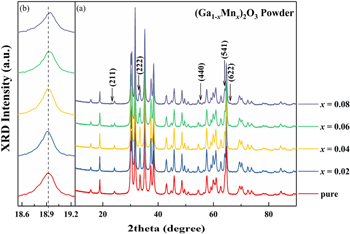
Figure 1. (a) XRD patterns of (Ga1−xMnx)2O3 powder, (b) magnified diffraction peaks near 2θ = 18.9º.
Download figure:
Standard image High-resolution imageFigure 2 exhibits XRD patterns of (Ga1−xMnx)2O3 thin films with different Mn content. All curves have been calibrated and normalized with the (0006) diffraction peak of sapphire substrate. Except diffraction peaks of the substrate, only three peaks around 19º, 38º, and 59º are observed. It can be seen that the peaks of the doped samples all shift to smaller 2θ compared with pure β-Ga2O3 thin film. Two cases of preferred orientation growth along β(−201) and γ(111) are marked with orange long dashed lines and purple short dashed lines, respectively. According to the previous experimental experience, we speculate that the doped thin films have undergone phase transition from β to γ phase.6 Fig. 2b also shows the enlarged diffraction peaks near 2θ = 18.9º. It can be found that, when x is just 0.02, there arises a large offset. Meanwhile, the doping of Mn at this low concentration will disturb the grain arrangement, resulting in the decrease of crystalline quality and the largen of full width at half maximum. Whereafter, with the increase of doping concentration, the peaks continue shifting to smaller 2θ, while the crystalline quality gradually gets better. Different from the XRD patterns of powder, there is no peak reverse migration phenomenon of the thin films until the doping concentration reaches x = 0.08. (The doping concentration values of thin films are about 2.46 at%, 4.40 at%, 6.34 at% and 8.64 at%, respectively, tested by the energy disperse spectroscopy. Considering that there might be slight host material loss during grinding and annealing, the Mn composition is almost similar with the concentration set by the target. More details could be found somewhere.20) It might be the result of the subsequent target pressing process and the high-temperature sintering process at 1273 K, which causes further successful incorporating of Mn element into the lattice of Ga2O3. However, even so, the inverse diffraction peak migration at x = 0.08 indicates that trace impurities are still inevitable in the thin film. Unfortunately, we still don't know what the impurities are.
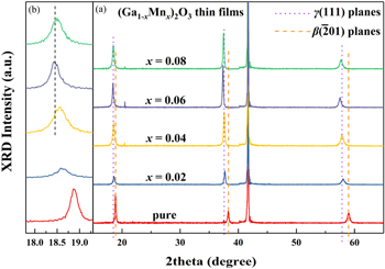
Figure 2. (a) XRD patterns of (Ga1−xMnx)2O3 thin films, (b) magnified diffraction peaks near 2θ = 18.9º.
Download figure:
Standard image High-resolution imageWe fix the XRD detectors angle at 2θ = 30.5º, rotate samples (φ = 0º ∼ 360º), and change the quadrant elevation of the test platform (χ = 0º ∼ 70º) to detect the X-ray pole figures of (Ga1−xMnx)2O3 thin films. As shown in Fig. 3, when x = 0.02, three sets of diffraction spots at χ = 25º, 35º and 55º are tested, mainly come from β(−401), γ(220) and β(002) planes, respectively, which means the film is composed of β and γ two phases.4 When x increases to 0.04 and 0.06, the diffraction spots of γ(220) planes at χ = 35º are more distinct, along with the disappearance of the β phase diffraction spots. But at the misaligned angle of about φ = 30º with the diffraction spots of γ(220) planes, a set of very faint diffraction spots is also detected, with the diffraction centre at χ = 55º. And as the doping concentration further increases, the twin-like diffraction spots at χ = 55º could be clearly detected in Fig. 3d. Unlike the pole figure of pure β-Ga2O3 thin film or β + γ mixed phase thin film, there exists an angular difference of in-plane angle φ.21 Although the diffraction centre is also at χ = 55º, the diffraction spots here appear in pairs like twin planes. Hence, we suspect that there are already other impurity phases in the film. The bigeminy of diffraction spots in the in-plane is very similar to the orthorhombic substances with three rotation domains, such as ε-Ga2O3, Mn2O3, MnO2 and MnO.22 Previously, we have drawn a wrong conclusion that (Ga0.96Mn0.04)2O3 thin film was β phase.20 At that time, there was not enough evidence to support the phase transition. Herein, it should be corrected that the film is γ phase.
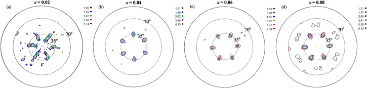
Figure 3. X-ray pole figures of (Ga1−xMnx)2O3 thin films as (a) x = 0.02, (b) x = 0.04, (c) x = 0.06, (d) x = 0.08.
Download figure:
Standard image High-resolution imageFigure 4 displays the top view surface SEM images of the thin films. It should be noted that, the wispy cracks among grains are caused by the gold spraying process before the test. As can be seen from the figures, the surface shows regular island growth with good uniformity in grain arrangement. The grain sizes fluctuate between 20 nm ∼ 5 nm.

Figure 4. SEM figures of (Ga1−xMnx)2O3 thin films as (a) x = 0.02, (b) x = 0.04, (c) x = 0.06, (d) x = 0.08.
Download figure:
Standard image High-resolution imageThe optical absorption depends on several factors, such as the crystalline quality, thickness of thin film, lattice strain, defects, and so on. Fig. 5a shows the typical absorbance spectra of (Ga1−xMnx)2O3 thin films (before annealing process). The optical bandgap is determined by extrapolating the linear region of the plot (αhν)2 vs hν and taking the intercept on the hν-axis, as shown in Fig. 5b.23 It is obvious that the absorption edges of Mn doped thin films significantly red shift and the optical bandgap reduce, mainly owing to new electron states in the bandgap introduced by Mn doping.24 Another phenomenon can be seen that, there are obvious Urbach band tails in most samples, which are commonly associated with amorphous states and variation of nano-systems in the vicinity of phase transitions.25,26 In addition, when x = 0.08, the sample also shows weak absorption in the visible light range especially higher than 600 nm, which may be related to other impurity phases existing in the film (the optical bandgap of Mn oxide is relatively narrow, for example, the bandgap of Mn3O4 is about 2.25 eV).
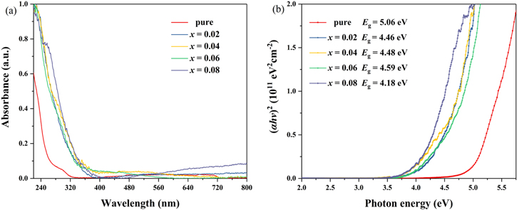
Figure 5. (a) UV-vis absorbance spectrum of (Ga1−xMnx)2O3 thin films and (b) the plot of (αhν)2 vs hν.
Download figure:
Standard image High-resolution imageThe structure diagram and microphysical drawing of (Ga1−xMnx)2O3 thin film based metal- semiconductor-metal PDs are shown in Fig. 6. This simple device structure is sufficed to study the effect of Mn dopant on the optoelectronic properties. And the Schottky contact can be basically realized after post annealing.27 The current-voltage (I-V) characters and time-dependent (I-t) photoresponse were measured by Keithely 2450. The I-t measurement was performed at a constant voltage of 10 V, with an 800 μW cm−2 excitation intensity ultraviolet (UV) lamp of 254 wavelengths as the light source.
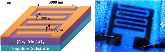
Figure 6. The schematic diagram (a) and microphysical drawing (b) of the interdigital electrode.
Download figure:
Standard image High-resolution imageFigure 7 shows the room temperature I-V characteristic of (Ga1−xMnx)2O3 thin films in dark condition. All curves have been artificially eliminated the zero drift caused by the contact between the electrode and the thin film. The inset is used to distinguish the I-V curves clearly. As for pure β-Ga2O3 thin film, the I-V curve is linear with a resistance of about 5.63 GΩ. While after Mn doping, the dark current increases, especially for the (Ga0.98Mn0.02)2O3 thin film. Its surface defect concentration is large, resulting in the resistance decreases significantly. The dark current of x = 0.04 & 0.06 PDs increases less. Under the bias voltage of 10 V, the dark current is still within 8 nA, and remain a high resistance value. However, in the I-V curves of these two thin films, an anomalous nonlinear pattern appears apparently. This behavior is similar to the dark current characteristics of (GaMn)2O3 thin film previously reported.18 We speculate the reasons may as follows: (1) the multivalent doping of Mn ion may introduce many new energy levels in the forbidden band and meanwhile cause local structural disorder. In addition, doping can induce phase transition, and there are intrinsic cation vacancies in the γ-Ga2O3. In the process of increasing bias voltage, the drift of vacancies becomes more and more obvious, and local impurity compensation occurs, which makes the carriers gradually saturated, as shown in Fig. 7d.28 (2) After annealing treatment, there may be weak junction at the interface between (Ga1−xMnx)2O3 and metal, and the carrier transport can be simply regarded as the process hindered by three parts of "junction-film-junction." When the bias voltage is low, the oxygen vacancies have not fully released the bound electrons, and the resistance of the thin film is large. Most of the partial voltage is equivalent to adding on the film. The macroscopic transport is mainly contributed by the carrier migration within the film, as shown in Fig. 7c. However, when the bias voltage increases, the concentration and migration rate of carriers gradually reach saturation, meanwhile the resistance of the film decreases. The effect of the junction on the overall transport process becomes more obvious, as shown in Fig. 7d, resulting in a similar resistive switching behavior.
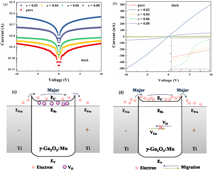
Figure 7. I-V characteristics of (Ga1−xMnx)2O3 PDs in dark condition, (a) logarithmic and (b) linear coordinates, (c) microcosmic mechanism diagram.
Download figure:
Standard image High-resolution imageWhen the PDs are vertically irradiated under the 254 nm UV light (800 μW cm−2), the photocurrent of all PDs increases obviously than dark condition. As shown in Fig. 8, the I-V curves confirm the existence of the junction: the photocurrent of Mn doped Ga2O3 thin films increases slowly first and then sharply with the increase of external bias, indicating that the thin films are Schottky-type contact with Ti/Au electrodes, exhibiting an obvious rectifying behavior. However, the photocurrent I-V curve of pure β-Ga2O3 PD is still linear mode, confirming that the contact is Ohmic type. Schottky-type optoelectronic device generally owns a high LDR, defined as Ip/Id, where Id is the dark current and Ip is the photocurrent. It can be estimated from the two I-V characteristic curves that at the voltage of 10 V, (Ga0.96Mn0.04)2O3 PD has the highest LDR of 6.89 × 10³, which is two orders of magnitude higher than the 19.16 of pure β-Ga2O3 PD.
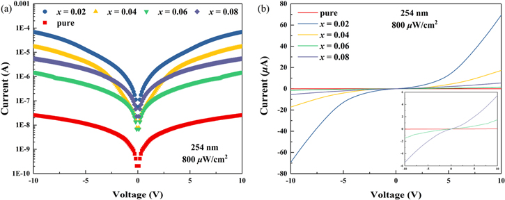
Figure 8. I-V characteristics of (Ga1−xMnx)2O3 PDs under 254 nm UV lamp, (a) logarithmic and (b) linear coordinates.
Download figure:
Standard image High-resolution imageTo further evaluate the performance of the PDs comparatively, Fig. 9 shows the I-t curves by on/off switching UV lamp every 60 s. It can be seen from Fig. 9a that most of the PDs maintain good stability during the test time of 600 s. After multiple illumination cycles, the devices still exhibit a nearly identical response, indicating the high robustness and good reproducibility. However, due to the existence of many defect states in the (Ga0.98Mn0.02)2O3 thin film, the photocurrent attenuation of this PD is very slow after turning off the UV irradiation lamp, and the original dark current value cannot be returned in the recovery time of 60 s. And with the passage of time, the photocurrent of the PD continues to rise slowly, indicating that its heat dissipation ability and stability are a little poor.

Figure 9. (a) I-t curves of the PDs, and the enlarged views in (b)–(f) are the corresponding fitting curves for the photocurrent rise and decay process of (a), respectively.
Download figure:
Standard image High-resolution image
The response time of PDs are shown in Figs. 9b–9f. The response (rise) edges and the recovery (decay) edges usually consist of two components with a fast response component and a slow response component.29 Generally, the fast response component comes from the rapid change of carrier concentration as soon as the illumination is turned on/off. The slow response component is caused by the carrier trapping/releasing, because of the existence of several defects in the thin films. A bi-exponential relaxation equation is used to quantitatively analyze the photocurrent rise and decay process of the PDs.30
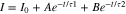
Where I0 is the steady state photocurrent, t is the time, A and B are two constants, and τ is the relaxation time constant. We define τr and τd as the time constants of the rise and decay edges, respectively. Herein, τ1 and τ2 correspond to the fast and slow part that has responded to 90% and the remaining 10%, respectively. By comparing the optoelectronic response curves of PDs with different doping concentrations, it can be seen that (Ga0.96Mn0.04)2O3 PD does have the shortest response time and the largest LDR.
In addition to response time and LDR, we also calculate the spectra responsivity (Rλ) and the external quantum efficiency (EQE), as shown in Table I. The formulas used are as follows:
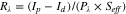

Where Pλ is the illumination intensity, Seff is the effective area, h is Planck's constant, c is the velocity of light, e is the electronic charge and λ is the wavelength of the light. Hence, the Rλ is defined as the photocurrent generated per unit power of incident light on the effective area of a PD, and the EQE is defined as the number of electrons detected per incident photon.
Table I. The characteristic parameters of (Ga1−xMnx)2O3 PDs.
| x | LDR | Rλ (A W−1) | EQE (%) | τr1 (s) | τd1 (s) |
|---|---|---|---|---|---|
| 0 | 19.16 | 0.69 × 10⁻³ | 0.34 | 0.899 | 0.682 |
| 0.02 | 1.53 × 10² | 1.97 | 963.53 | 2.154 | 0.768 |
| 0.04 | 6.89 × 10³ | 0.50 | 244.55 | 0.606 | 0.081 |
| 0.06 | 2.50 × 10² | 0.04 | 19.56 | 0.956 | 0.674 |
| 0.08 | 75.09 | 0.15 | 73.37 | 0.973 | 0.675 |
It can be seen that the performance of the PDs can be effectively improved through the modulation of Mn doping on the bandgap and carrier concentration. As for the (Ga0.98Mn0.02)2O3 thin film, owning a β + λ mixed phase and more defects, showing a higher dark current, a lower LDR and a slower response speed. However, the existence of the defect energy levels at gap edge makes it easier for transition, and improves the Rλ and EQE of the PD.31 Owning better crystalline quality, the (Ga0.96Mn0.04)2O3 thin film has the lowest dark current, the highest LDR, and the fastest response time in all Mn doped Ga2O3 thin films. It indicates that there are fewer traps in the film or near the junction, which does not affect the overall optoelectronic properties of the PD to a great extent. However, with the further increase of the doping concentration, the performance decreases slightly. Based on the above results, it can be concluded that the doping concentration of about 4 at% is approximately the optimal solution in our experimental system.
The comparisons between the (Ga0.96Mn0.04)2O3 thin film in this work with other Ga2O3 PDs are listed in Table II. Since the optoelectronic performance of a semiconductor PD can be influenced by so many factors, such as the nanostructure, electrode size, dopants, bias voltage, and so on. Herein, we only focus on the performance parameters of some doped Ga2O3 thin film PDs with symmetrical Ti electrodes and metal-semiconductor-metal (MSM) structure. It can be seen that, in some aspects the performance of our γ-(Ga0.96Mn0.04)2O3 thin film PD could be comparable to that of other doped Ga2O3 polymorphs. According to these results, we believe that the γ-Ga2O3 thin films are promising to obtain high quality PDs. While ensuring the response speed and LDR of PDs, more work needs to do on achieving high responsivity and high EQE.
Table II. Optoelectronic responses of doped Ga2O3 thin film PDs with symmetrical Ti electrodes and MSM structure.
| Type | Rλ (A W−1) | EQE (%) | Id (A) | LDR | τd (s) |
|---|---|---|---|---|---|
| γ-Ga1.92Mn0.08O3 | 0.5 | 2.4 × 10² | 10−9@10 V | 6.9 × 10³ | 0.08 |
| β-Ga0.94Mn1.06O318 | 7 × 10⁻² | 36 | 10−9@10 V | 67.1 | 0.28 |
| β-Ga0.75In0.25O332 | 30 | 1.5 × 10⁴ | 10−10@10 V | 103 | 0.1 |
| β-Ga1.9Mg0.1O333 | 2.4 × 10⁻² | 11.6 | 10−12@10 V | 104 | 0.02 |
| β-Ga1.8Sn0.2O334 | 3.6 × 10⁻² | 17.6 | 10−8@50 V | 20.6 | 0.94 |
| α-Ga1.8Sn0.2O335 | 9.6 × 10⁻² | 46.7 | 10−9@50 V | 1.4 × 10² | 7.3 |
| ε-Ga1.98Sn0.02O336 | 3.74 | 1.8 × 10³ | 10−10@20 V | 105 | 0.16 |
Conclusion
The γ-(Ga1−xMnx)2O3 thin films with different doping concentrations were prepared on sapphire substrates by using the laser molecular beam epitaxy technology. The effect of Mn dopant on the structural, micro-morphologic and optoelectronic properties of the thin films have been systematically studied. The results show that the crystalline quality and the solar blind optoelectronic detection performance all increased first and then decreased with the further increase of doping concentration. When x = 0.04, the PD has the lowest dark current, the highest LDR and the shortest response time. Its excellent physical properties are mainly due to the optimization of Mn doping on the crystalline quality, bandgap and carriers of thin film.
Acknowledgments
This work was supported by the National Natural Science Foundation of China (grant Nos. 61774019, 51572033, and 51572241), the Beijing Municipal Commission of Science and Technology, China (grant No. SX2018-04), the Fund of State Key Laboratory of Information Photonics and Optical Communications (BUPT), and the Fundamental Research Funds for the Central Universities.