
Abstract
The β-Ga2O3 nanomembrane (NM)/diamond heterostructure is one of the promising ultra-wide bandgap heterostructures that offers numerous complementary advantages from both materials. In this work, we have investigated the thermal properties of the β-Ga2O3 NM/diamond heterostructure with three different thicknesses of β-Ga2O3 nanomembranes (NMs), namely 100 nm, 1000 nm, and 4000 nm thick β-Ga2O3 NMs using Raman thermometry. The thermal property—temperature relationships of these β-Ga2O3 NM/diamond heterostructures, such as thermal conductivity and interfacial thermal boundary conductance were determined under different temperature conditions (from 100 K to 500 K with a 40 K interval). The result provides benchmark knowledge about the thermal conductivity of β-Ga2O3 NMs over a wide temperature range for the design of novel β-Ga2O3-based power electronics and optoelectronics.
Export citation and abstract BibTeX RIS
In recent years, β-Ga2O3 has attracted significant attention as a next-generation ultra wide-bandgap semiconductor, due to its exceptional material properties including a wide bandgap (∼4.9 eV), a large electrical breakdown voltage (∼8 MV cm−1), lattice compatibility with other wide bandgap semiconductors, such as, β-Ga2O3/ZnO, β-Ga2O3 and SiC, and large area affordable substrates grown from melt by the floating zone and edge-defined film-fed growth methods.1–3 All of these properties enable β-Ga2O3 to be used for various future electronic applications such as high-frequency devices, deep-ultraviolet optoelectronics, and high-power applications, in which the thermal properties play a critical role for their operation. However, the thermal conductivity of β-Ga2O3 is substantially lower than that of other wide bandgap semiconductors; namely, the thermal conductivity of bulk β-Ga2O3 is 20 ∼ 30 W m−1·K−1 vs AlN (200 W m−1 k−1),4 SiC (387 W m−1 K−1),5 jGaN (∼170 W m−1 K−1),6 and diamond (>2000 W m−1 K−1).7,8 Furthermore, unlike most of the other wide bandgap semiconductors, the thermal conductivity of β-Ga2O3 varies by ∼30% depending on the crystal orientation due to the anisotropic property from the monoclinic lattice structure.9–11 To overcome the poor thermal property of β-Ga2O3, a couple of novel structures have been proposed that use heterogeneous integration methods.12–14 Another recent approach has utilized the superior thermal property of diamond by forming a heterostructure between β-Ga2O3 and diamond.7,14,15 In fact, a diamond layer has been used as a heat dissipator in various electronic applications16 due to its superior thermal management capabilities such as a high thermal conductance, and low thermal expansion.7,8 Also, the heterostructure using n-type β-Ga2O3 and p-type diamond can form an ultra-wide bandgap p-n junction that can be used as a basic building block for the future ultra-wide bandgap electronic application. Thus, accurate characterization of the thermal property of β-Ga2O3 on a diamond substrate and β-Ga2O3/diamond heterostructure is crucial for designing future high-power electronics or ultra-violet optoelectronics. However, several challenges must be addressed to accurately characterize the thermal property of β-Ga2O3 itself and the β-Ga2O3/diamond heterostructure.
The first issue is related to the growth of a high-quality β-Ga2O3/diamond heterostructure. As is known, the lattice parameters of β-Ga2O3 (3.04 Å to the b-axis and 5.8 Å to the c-axis) and diamond (3.57 Å) are very different.14 Thus, direct growth is not possible. Instead, a synthesis of quasi-two-dimensional β-Ga2O3, also called β-Ga2O3 nanomembranes (NMs), can be created from the bulk substrate using a well-known scotch tape method.17,18 However, when it comes to the formation of a β-Ga2O3/diamond heterostructure, a rough diamond surface does not allow for the formation of a seamless contact in their hetero-interface, and thus it often leads to the inaccurate thermal property of the β-Ga2O3/diamond heterostructure.
Another, perhaps more critical, issue is the characterization method. Conventionally, there are two categories of characterization methods by which to measure the thermal property of materials: (1) steady-state methods such as the 3ω-method,19,20 and (2) transient state methods such as the Time-Domain Thermo-Reflectance (TDTR) method,14 the transient hot-wire method,21–23 the transient plane source method, and the transient line source method. Typical steady-state methods require additional microfabrication steps to deposit electrodes on the specimen which is not available on soft- or liquid samples. Also, it is difficult to avoid errors in the thermal property characterization due to the additional phonon scattering caused between electrodes and the sample surface or the unwanted scattering of light especially when the sample has multiple layers. The transient state methods do not need any pre-calibration or contacts to measure the thermal conductivity, but these methods are available only with the homogenous samples. Thus, these methods do not offer accurate thermal property characterization when the samples have multi-layer structures or an anisotropic thermal property. Recently, a group of research teams reported the thermal conductivity of β-Ga2O3 using methods such as the 3ω-method and the TDTR method.14,24 While these reports have provided a guideline about the thermal property of β-Ga2O3, it is inevitable to have small errors due to the aforementioned issues.
In this work, we investigated thermal conductivity of three types of (−201) β-Ga2O3 NMs from β-Ga2O3/diamond heterostructures using Raman thermometry under different temperature condition from 100 K to 500 K with a 40 K interval. To accurately characterize the thermal property of β-Ga2O3 NMs/diamond heterostructures, we have employed polished single crystalline diamond substrates that showed atomically smooth surface roughness, less than 1 nm. These samples were carefully measured using a micro-Raman spectroscopy-based thermometry (also called Raman thermometry) with the additional light intensity control module. Raman thermometry offers several advantages in terms of thermal conductivity measurement as compared to other methods; (1) the Raman peak shift is extremely sensitive to heat, because it can capture subtle changes in molecular vibration and, thus, provide higher precision in the measurement of thermal conductivity. (2) Raman thermometry offers a means of measuring thermal conductivity along the cross-plane or in-plane direction due to the freedom of the moving stage and controllable focus depth. (3) Lastly, it offers a simple and easy way to characterize the thermal property as compared to other methods, because Raman thermometry is based on micro-Raman spectroscopy.
To reveal the thermal property of β-Ga2O3 NMs/diamond heterostructures with different β-Ga2O3 NMs thicknesses, we prepared three different (100) β-Ga2O3 NM samples—namely, 100 nm-, 1000 nm-, and 4000-nm-thick β-Ga2O3 NMs—from a (−201) β-Ga2O3 substrate using a mechanical exfoliation method and then carefully transfer-printed them onto single crystalline diamond substrates. A series of Raman spectroscopy characterizations was performed under different temperature conditions and Raman laser intensities using 5× and 20× objective lenses to apply different heat flexes to β-Ga2O3 NMs. The thermal property/temperature relationship of these β-Ga2O3 NM/diamond heterostructures was revealed and compared our values with other reported values to discuss the multi-dimensional thermal properties-β-Ga2O3 NM thickness-doping concentration relationship.
Experimental
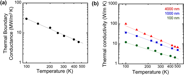
As shown in Fig. 1, the sample preparation started with a (−201) β-Ga2O3 (Sn doped with 1 × 1018 cm−1 donor concentration; Novel Crystal Technology). Firstly, the wafer was cleaved into a small piece, followed by mechanical exfoliation using a well-known Scotch tape method16,17 (Fig. 1a(i)) In this stage, a typical thickness of β-Ga2O3 became several micrometer ranges and such a thin- and freestanding- single crystalline material is called β-Ga2O3 NMs.16 We repeated the exfoliation until the desired thicknesses, namely 4000 nm, 1000 nm, and 100 nm, respectively were achieved. To accurately measure the thickness of β-Ga2O3 NMs, a three-dimensional surface profilometer (Profilm3D Filmetric) was used which has a spatial resolution of less than 5 nm (Fig. S1a is available online at stacks.iop.org/JSS/9/055007/mmedia). It should be noted that the surface crystal orientation became (100) after exfoliation because β-Ga2O3 has a relatively weaker bonding toward a (100) direction as compared to other directions. When the desired thickness was achieved, free-standing β-Ga2O3 NMs were carefully transfer-printed onto a single crystalline diamond substrate (undoped (100) diamond) using an elastomeric stamp (PDMS, Polydimethylsiloxane) as depicted in Fig. 1a(ii)–(v).25–27 This micro transfer-printing method did not use any adhesive between β-Ga2O3 NM and the diamond substrate. Thus, to enable intimate contact between β-Ga2O3 NMs and the diamond substrate, it is critical to have an extremely smooth surface roughness. Failure to achieve a smooth diamond surface often results in an incorrect thermal property due to increased phonon scattering at the rough hetero-interface.28–30 As shown in Fig. S1b in the supporting information, the average root-mean-square surface roughness of both polished diamond substrate and an exfoliated β-Ga2O3 NM surface measured using an atomic force microscope (AFM) were found to be below 1 nm, thus it was possible to create a high-quality β-Ga2O3 NMs/diamond heterostructure. Also, to further improve the accuracy of the thermal characterization, we focused the Raman laser at the center of β-Ga2O3 NMs and tried to avoid any particles which are accidently trapped between β-Ga2O3 NMs and diamond. Prior to the transfer-printing step, the diamond substrate was thoroughly cleaned using an ammonium sulphuric acid solution for 30 min at 200 °C and then rinsed in an ammonium hydroxide/hydrogen peroxide solution, followed by a deionized (DI) water rinse to obtain a contaminant-free and native oxide-free surface.31 The samples were annealed at 300 °C for 1 min in the rapid thermal annealing (RTA) system to enhance the bonding strength.32,33 This annealing condition was carefully chosen by considering the thermal expansion coefficient of β-Ga2O3 NMs and diamond. Finally, samples were ready to measure thermal conductivity. A micro-Raman spectroscopy (Renishaw Raman spectroscopy) was carried out to inspect the initial quality of β-Ga2O3 NM/diamond heterostructures as shown in Fig. 1b. Raman peaks in Fig. 1b that are distributed from 180 cm−1 to 800 cm−1 are responsible for β-Ga2O3 NM and a strong peak located at 1332 cm−1 is responsible for single crystal diamond.17,31 No sign of Raman peak shifting also confirmed that there was no residual strain in β-Ga2O3 NM from the integration process.

Figure 1. (a) A schematic illustration of the sample preparation process: (i) mechanical exfoliation of β-Ga2O3 NMs from β-Ga2O3 substrate, (ii)–(iv) micro-transfer printing of β-Ga2O3 NMs onto single crystalline diamond substrate, (v) (top) a microscopic image of transfer-printed β-Ga2O3 NM on diamond and (bottom) its cross-sectional illustration. (b) a Raman spectrum taken from the β-Ga2O3 NM/diamond heterostructure showing its distinctive Raman modes. (c) illustration of the Raman thermometry setup and direction of the Raman laser beam.
Download figure:
Standard image High-resolution imageResults and Discussion
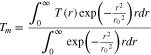
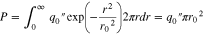
The thermal conductivity measurement uses local heating by laser illumination under different power intensities of the green (532 nm) Raman laser (from 0 to 20 mW for a 5× objective lens and from 0 to 10 mW for a 20× objective lens), and corresponding Raman peak shifting under different temperature conditions (from 100 K to 500 K with a 40 K interval). Therefore, it is essential to measure the actual power levels of Raman laser on the sample surface and the heating rate that involves the spot size and corresponding light intensity prior to the actual thermal conductivity measurement. The measurement of the heating rate began with the measurement of the Raman laser spot size and corresponding light intensity. Firstly, laser spot sizes were measured at the edge of a Si wafer under different objective lenses using Raman spectroscopy and an error function,34 yielding laser spot diameters of 1.5 μm, and a 2.5 μm for 20× and 5× objective lenses, respectively. These spot diameters were much smaller than the width of β-Ga2O3 NM (∼40 μm); therefore, it was possible to locate the Raman laser beam spot at the center of β-Ga2O3 NM during a Raman spectroscopy measurement. To accurately realize the desired power level, a disk-type linear variable filter (Edmond optics) was installed at the bottom of the Raman objective lens to precisely adjust the desired beam power level, which provided a continuous variable transmittance from 0% to 100%. Figure 1c shows a schematic illustration of the Raman thermometry setup used in this experiment. Once actual laser power intensity values were measured, the temperature distribution of β-Ga2O3 NM was obtained by the heat diffusion equation in the cylindrical coordinate by Eq. 135:

where r, g, and Ks represent the radius of the beam spot, the interfacial thermal boundary conductance and the thermal conductivity of β-Ga2O3 NM. Given bandgap (4.9 eV) of β-Ga2O3 NM, a 5% of actual light absorption in β-Ga2O3 NM at 532 nm was considered in this calculation from the known absorption coefficient of β-Ga2O3.36 We also assume that the heat flux is distributed in a Gaussian profile.35,37 Thus, the local temperature distribution was calculated from the Gaussian heat distribution using the measured laser spot diameter and Eq. 235:
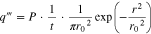
Assuming a Gaussian profile and a laser spot radius of r0, this can be used to calculate the volumetric heating power density  as shown in Eq. 335:
Once the laser spot diameters with 5× and 20× objective lenses and the heating rate were determined, the β-Ga2O3 NMs/diamond heterostructures with different β-Ga2O3 NM thicknesses were placed on the stage in the vacuum chamber of the Raman thermometry system at a base pressure of 1 × 10⁻⁵ mtorr. A series of Raman thermometry was performed under different temperature conditions (from 100 K to 500 K with a 40 K interval). As described in the experimental section, three samples that had different β-Ga2O3 NM thicknesses namely, 100 nm, 1000 nm, and 4000 nm (labeled as samples #1, #2, and #3 hereafter) were measured under full laser intensity using 5× and 20× objective lenses at each temperature condition (20 mW for the 5× objective lens and 10 mW for the 20× objective lens respectively). Figures 2a–2c show the Raman spectra from each β-Ga2O3 NMs/Diamond heterostructure measured from 100 K (blue) to 500 K (red) with 40 K intervals. After the raw Raman spectra were captured, we traced the shifting of the Raman peak at 199 cm−1, which was caused by a libration of Ga-O bonding as a function of the sample temperature using 5× and 20× objective lenses separately to calculate a degree of Raman shifting as shown in Figs. 2d–2f. It should be noted that the Raman mode at 199 cm−1 was chosen in this experiment because it is one of the most dominant Raman modes in β-Ga2O3 NM, however this method also works with other distinctive Raman modes such as A3g mode at 201 cm−1, A5g mode at 347 cm−1 and A6g mode at 416 cm−1.17 Figures 2d–2f indicate the Raman shift as a function of temperature. The shifting rates of the Raman peak for samples #1 ∼ #3 were −0.7 cm−1/10 K, −0.21 cm−1/10 K, and −0.06 cm−1/10 K with the 5× objective lens and −0.16 cm−1/10 K, −0.12 cm−1/10 K, and −0.03 cm−1/10 K with the 20× objective lens, respectively.

Figure 2. (a)–(c) Three-dimensional Raman spectra taken under different temperature conditions (100 K ∼ 500 K with 40 K intervals) from samples #1 ∼ #3, respectively. (d)–(f) a slope of the Raman peak captured from Ga-O bonding at 199 cm−1 under different temperature conditions using a 5× objective lens (denoted as an R1 slope) and a 20× objective lens (denoted as an R2 slope) from samples #1 ∼ #3, respectively.
Download figure:
Standard image High-resolution imageThen, the Raman shift with respect to the stage temperature with six different laser powers was measured. From a set of Raman spectra measured under different laser powers (from 0 mW to 20 mW for the 5× objective lens and from 0 to 10 mW for the 20× objective lens) and temperature conditions (from 100 K to 500 K) shown in Figs. S2–S4 in supporting information, the rate of the Raman peak shifting was calculated as shown in Fig. 3. Similar to Figs. 2d–2f, Raman shifts measured from samples #1 ∼ #3 with respect to the laser power from 1 mW to 18 mW and from 100 K to 500 K using the 5× and 20× objective lenses were plotted to calculate the slopes. For the Raman spectroscopy with a 5× objective lens, a maximum laser power of 20 mW was used, while a maximum laser power of 10 mW was used with a 20× objective lens due to the different numerical aperture value of the 5× objective lens and the 20× objective lens. The temperature increase in the optically heated β-Ga2O3 NM causes the red-shift of the Raman peaks due to Ga–O bond softening.35,38–40 It should be noted that the use of different objective lenses generates different heating intensity as we discussed in the previous section, thus, the degrees of Raman shifting were also different. The shifting rates of the Raman peak with respect to the laser power for samples #1 ∼ #3 were measured to be −0.05324 cm−1 mW−1, −0.02179 cm−1 mW−1, and −0.01 cm−1 mW−1 with the 5× objective lens and −0.11 cm−1 mW−1, −0.064 cm−1 mW−1, and −0.03 cm−1 mW−1 with the 20× objective lens, respectively.
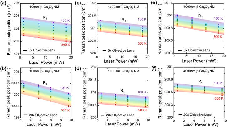
Figure 3. (a)–(b) A slope of the Raman peak captured from Ga–O bonding at 199 cm−1 under different temperature and illumination conditions using (a) a 5× objective lens (denoted as an R3 slope) and (b) a 20× objective lens (denoted as an R4 slope) from sample #1. Figure (c)–(d) and (e)–(f) are the same types of plots taken from samples #2 and #3, respectively. The color gradient denotes the changes in temperature from 100 K (purple) to 500 K (red).
Download figure:
Standard image High-resolution imageAfter the extraction of two different slope values, namely (1) the Raman peak shifting rate vs. the temperature (denoted as R1 and R2 in Fig. 2), and (2) the Raman peak shifting rate vs. the temperature-laser intensity (denoted as R3 and R4 in Fig. 3), the calculation for thermal conductivity and interfacial thermal boundary conductance started with Eq. 1, as g and Ks represent the interfacial thermal boundary conductance and the thermal conductivity, respectively, here the thermal conductivity Ks represents the directionally averaged thermal conductivity. For the samples with different β-Ga2O3 NM thicknesses, t. In Eq. 4,  denotes a volumetric heating power density in the Gaussian profile.32
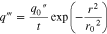
where q0‴ is the peak absorbed laser power per unit area at the center of the laser spot. The total absorbed laser power, P, is calculated by Eq. 535:
and q0'' can be rewritten as Eq. 6:

Then, the temperature increase in the β-Ga2O3 NM was calculated using Eq. 2. With the use of  and
and  Eq. 1 becomes a nonhomogeneous Bessel's equation (Eq. 7)35:

The solution to Eq. 7 is given as35,41:

where the two homogeneous solutions I0(z) and K0(z) are the zero-order modified Bessel functions of the first and second kinds, respectively. We then define the measured thermal resistance as Rm' = Tm/P. Based on Eqs. 2 and 5, Eq. 9 can be derived35,41:
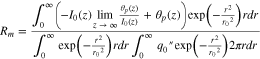
Given the input power and laser spot size, compared with the two sets of slopes from Figs. 2 and 3: (1) slopes from Raman shifting with respect to temperature using 5× (R1) and 20× (R2) objective lenses and (2) slopes from Raman shifting with respect to light intensity using 5× (R3) and 20× (R4) objective lenses. From each sample, we can define Rm' = Tm/P = R4/R2 and Rm'' = R3/R1, respectively. Based on the ratio of Rm values, we can calculate the ratio of g/Ks, which depends only on the ratio of the two Rm values (Rm'/Rm'').42 Once the ratio of g/Ks was calculated, the Ks and g values can be further determined by choosing one set of objective lens' results, which yields the room-temperature g values of 7.58 MW/(m2·K). We repeated the calculation under different temperature conditions and plotted the thermal boundary conductance-temperature relationship from 100 K to 500 K as shown in Fig. 4a. The higher interfacial thermal boundary conductance is attributed to multiple factors.43 It is known that the thermal transport property across the heterostructure, particularly the one formed with a van der Waals interface, is largely affected by the interface quality, namely the lower surface roughness and surface energy because these factors reduce phonon transmission across the heterointerface and, thus lower thermal boundary conductance. Therefore, it is important to achieve intimate contact and maintain sufficiently high surface energy at the heterointerface in order to enhance phonon transmission. In our case, the atomically smooth diamond and β-Ga2O3 NM surface helps increase the interfacial thermal boundary conductance and facilitate the heat dissipation of β-Ga2O3 NMs through the diamond substrate. The extracted interfacial thermal boundary conductance values suggest that the diamond substrate is highly capable of heat dissipation, which is comparable to epi-structures based on other wide bandgap semiconductors such as GaN-on-SiC (3.3 MW/(m2·K)),44 GaN-on-sapphire (12 MW/(m2·K)).44 Therefore, the β-Ga2O3 NM/diamond heterostructure offers a viable route for dissipating heat from β-Ga2O3 NM so as to effectively complement the poor thermal property of β-Ga2O3.
Figure 4. (a) Thermal boundary conductance of β-Ga2O3 NM/diamond hetero-interface with respect to temperature from 100 K to 500 K and (b) thermal conductivity of 100 nm-, 1000 nm-, and 4000 nm- thick β-Ga2O3 NMs with respect to temperature from 100 K to 500 K, respectively.
Download figure:
Standard image High-resolution image
Finally, as shown in Fig. 4b, the thermal conductivity values of samples #1 ∼ #3 with respect to temperature were extracted. The thermal conductivity—temperature relationships of these β-Ga2O3 NMs were revealed to be 12 W m−1·K−1, 36.4 W m−1·K−1, and 100.86 W m−1·K−1 at 100 K for 100 nm, 1000 nm, and 4000 nm thick β-Ga2O3 NMs, respectively. These were gradually decreased to 3.1 W m−1·K−1, 8.68 W m−1·K−1, and 13.97 W m−1·K−1 at room temperature. This trend can be explained by the phonon–phonon scattering rate is sensitive to temperature because fewer numbers of states are occupied. When thickness of β-Ga2O3 NM gets thinner, the additional film boundary forms. In this case, the phonon mean free paths become relatively smaller, thus phonon transport is decided primarily by phonon scattering processes occurring at the boundaries of β-Ga2O3 NM, which results in smaller thermal conductivity.
Conclusions
In conclusion, we have successfully measured the thermal conductivity of three types of (−201) β-Ga2O3 NMs using Raman thermometry under different temperature conditions from 100 K to 500 K with 40 K intervals. To investigate the thermal conductivity of β-Ga2O3 with different thicknesses, three different thicknesses of (100) β-Ga2O3 NM—namely, 100 nm, 1000 nm, and 4000 nm—were prepared from a (−201) β-Ga2O3 substrate using a mechanical exfoliation method and then transfer-printed onto the single crystalline diamond substrates. The thermal conductivity/temperature relationships of these β-Ga2O3 NMs were revealed to be 12 W m−1·K−1, 36.4 W m−1·K−1, and 100.86 W m−1·K−1 at 100 K and gradually decreased to 3.1 W m−1·K−1, 8.68 W m−1·K−1, and 13.97 W m−1·K−1 at room temperature for 100-nm-, 1000-nm-, and 4000-nm-thick β-Ga2O3 NMs, respectively. Our results provide benchmark knowledge about the thermal conductivity of β-Ga2O3 NMs over a wide temperature range for the design of novel β-Ga2O3-based power electronics and optoelectronics.
Acknowledgments
This work was supported by the National Science Foundation (grant number: ECCS-1809077) and partially by the seed grant by Research and Education in energy, Environment, and Water (RENEW) Institute and Center of Excellence in Materials Informatics (CMI) at the University at Buffalo.