
Abstract
Tin (Sn)-doped beta phase gallium oxide (β-Ga2O3) nanostructures at different Sn concentrations (0 to 7.3 at%) are synthesized using a facile hydrothermal method. The Sn-doped β-Ga2O3 nanostructures are characterized using scanning electron microscopy, transmission electron microscopy, energy dispersive X-ray spectroscopy, X-ray powder diffraction, X-ray photoelectron spectroscopy, and absorbance spectroscopy. In addition, their photocatalytic activity is evaluated by observing methylene blue degradation under ultraviolet light (254 nm) irradiation. The photocatalytic activity of the Sn-doped (0.7 at%) β-Ga2O3 nanostructures is significantly enhanced compared to that of intrinsic β-Ga2O3 nanostructures due to the elevated charge separation. Excessive Sn concentrations (exceeding 2.2 at%) above the solid solubility limit of the Sn in β-Ga2O3 nanostructures lead to SnO2 and SnO precipitation. The presence of SnO2 and SnO degrades the photocatalytic efficiency in the β-Ga2O3 nanostructures. The results suggest new opportunities for the synthesis of highly effective β-Ga2O3-based photocatalysts for applications in environmental remediation, disinfection, and selective organic transformations.
Export citation and abstract BibTeX RIS

This is an open access article distributed under the terms of the Creative Commons Attribution 4.0 License (CC BY, http://creativecommons.org/licenses/by/4.0/), which permits unrestricted reuse of the work in any medium, provided the original work is properly cited.
Semiconducting beta phase gallium oxide (β-Ga2O3) has gained significant interest in power electronic applications due to its wide bandgap of ∼4.9 eV.1–3 In addition to applications in power electronics, β-Ga2O3 can be used as an effective photocatalyst under ultraviolet-C (UVC) light irradiation.4–7 The photocatalytic properties of β-Ga2O3 under UVC have been investigated for environmental applications such as the removal of volatile organic compounds (VOCs).8,9 Several studies have claimed that the photocatalytic properties of β-Ga2O3 outperformed those of conventional TiO2 under UVC light8,9 due to the higher redox ability of photo-generated electron and hole pairs (EHPs); the bandgap energy of Ga2O3 (∼4.9 eV) is higher than that of TiO2 (∼3.3 eV).10
In general, photocatalytic efficiency increases with the surface area of photocatalysts because the photocatalytic reaction occurs on the catalyst's surface. Rationally designed nanostructures with a relatively larger effective surface area are more beneficial than bulk materials as photocatalysts. Various β-Ga2O3 nanostructures including nanowires, nanorods, nanobelts, and nanoflakes have been developed using both physical and chemical approaches, and their photocatalytic activity has been presented.11–14 On top of the surface area, a variety of modification strategies, including crystalline faces, defect types, and dopants, have also been controlled to further enhance the photocatalytic properties of nanostructures.15,16
Recently, it has been reported that the addition of dopants could improve the photocatalytic efficiency of a β-Ga2O3 nanostructure, which requires additional machines and processes to realize doped photocatalysts.17,18 In this work, we report a facile approach to synthesize Sn-doped β-Ga2O3 nanostructures using a hydrothermal method. We also investigate the photocatalytic characteristics of the Sn-doped β-Ga2O3 nanostructures with different Sn concentrations.
Experimental
Synthesis of Sn-doped β-Ga2O3 nanostructures
The detailed experimental procedure used to form the β-Ga2O3 nanostructures via the hydrothermal process, as well as the method of photocatalytic evaluation, have been described in previous reports.9,17 First, 0.1-M gallium (III) nitrate hydrate (Ga(NO3)3·xH2O) was dissolved in 50 ml of deionized (DI) water under magnetic stirring at room temperature. The pH of the clear solution was 2.5, and this eventually resulted in the formation of intrinsic β-Ga2O3 nanostructures through the hydrothermal reaction.12 Next, to form Sn-doped β-Ga2O3 nanostructures at different Sn concentrations, different amounts of liquid phase SnCl4 (0.026, 0.052, 0.130, and 0.260 g for 0.7, 2.2, 2.9, 3.2, and 7.3 at% of Sn dopants, respectively) were added to the prepared solution. The Sn concentrations in β-Ga2O3 nanostructures were determined using an X-ray photoelectron spectroscopy (XPS) analysis. An ammonium hydroxide solution ((NH4(OH) 28 vol% in H2O) was subsequently added in the mixed solution on a hot plate at 60 °C to maintain the pH balance at around 10 because β-Ga2O3 nanostructures would have formed at a pH exceeding 8.19 The supersaturated mixed solution was transferred to a Teflon-lined stainless-steel autoclave that was sealed, heated in an electric oven at 140 °C for 10 h, and cooled down naturally to room temperature.17 After the hydrothermal synthesis process, the collected nanostructures were washed several times with DI water to remove residual reagents and then dried in an oven at 70 °C for 6 h. Sn-doped β-Ga2O3 nanostructures at different Sn concentrations were finally formed after annealing the nanostructures in O2 ambient at 1000 °C for 6 h.
Characterization of Sn-doped β-Ga2O3 nanostructures
The material properties of Sn-doped β-Ga2O3 nanostructures with different Sn concentrations were characterized using scanning electron microscopy (SEM, Hitachi, Su-70), transmission electron microscopy (TEM, JEOL, JEM-2100F), energy dispersive X-ray spectroscopy (EDS), X-ray powder diffraction (XRD, PANalytical, X'pert pro), and X-ray photoelectron spectroscopy (XPS, Thermo Fisher Scientific, K-ALPHA + System). The area under the curve (Lorentzian) in the XPS peaks was used to quantify the particular atomic concentration and states of nanostructures. The bandgap of each nanostructure was extracted using diffuse reflectance spectroscopy (DRS, SHIMADZU, SolidSpec-3700) via the expression of (αhν)m vs hν, where α is the absorption coefficient, h is the Planck constant, and ν is the frequency of the electromagnetic radiation. For the case with the intrinsic/Sn-doped β-Ga2O3 nanostructures, m = 2 was used because β-Ga2O3 nanostructures have been reported to exhibit optical properties close to those of direct bandgap materials.20
Photocatalytic activity of Sn-doped β-Ga2O3 nanostructures
The photocatalytic activity of Sn-doped β-Ga2O3 nanostructures with different Sn concentrations was evaluated by measuring the photodegradation of methylene blue (MB) dye, a model system, in an aqueous solution.21 For each sample, 4 mg of Sn-doped β-Ga2O3 nanostructures at different Sn concentrations were homogeneously dispersed in the 4-ml MB solution (1.56 mg l−1 in DI water), which was then exposed under a 254-nm light at 6 W for 20 min. After the β-Ga2O3 nanostructures were filtered through a syringe filter (0.45 μm), the absorbance of the MB solution was analyzed using UV–vis spectrophotometers (SHIMADZU, UV-3600), and an intact MB solution (without β-Ga2O3 nanostructures and not irradiated) was used as a control for comparison.
The absorption spectrum of the MB solution itself shows two strong absorption peaks centered at 610 and 664 nm, which are the absorptions of dimers and monomers of MB cations, respectively.22 The photogenerated charge carriers (electrons and holes) in a catalyst in the MB solution can generate OH radicals, which are one of the major radical types that decompose the MB. Thus, after the UV irritation of the MB solution, the absorptions at these two peaks are substantially reduced depending on the photocatalytic efficiency of the catalyst. In this work, the photocatalytic activity (%) of the Sn-doped β-Ga2O3 nanostructures at different Sn concentrations was quantitatively determined with (1),
where Ci and C are the absorbance at λ = 664 nm for the intact MB solution and the UV-irradiated MB solution in the presence of Sn-doped β-Ga2O3 nanostructures at different Sn concentrations, respectively.
Results and Discussion
Figure 1 exhibits SEM images of the β-Ga2O3 nanostructures with different Sn concentrations from 0 to 7.3 at%. The images showed that the intrinsic β-Ga2O3 nanostructures consisted of both rice-like nanostructures and nanorods. As the Sn concentration increased, the nanorods became thicker and longer and eventually turned into microrods. On the other hand, the rice-like nanostructures tended to be thinner and narrower with the Sn concentration. When the Sn concentration in the β-Ga2O3 nanostructures exceeded 3.2 at%, no rice-like nanostructures were observed, and only microrods of prism-like crystals were observed along with nanoparticles.
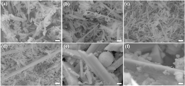
Figure 1. SEM images of β-Ga2O3 nanostructures with Sn concentrations of (a) 0 at%, (b) 0.7 at%, (c) 2.2 at%, (d) 2.9 at%, (e) 3.2 at%, and (f) 7.3 at% (scale bar: 1 μm). After hydrothermal synthesis, the nanostructures were calcined at 1000 °C for 6 h.
Download figure:
Standard image High-resolution imageFigures 2a–2h exhibit TEM and EDS elemental mapping images of the Sn-doped β-Ga2O3 nanostructures with the Sn concentration of 0.7 and 2.2 at%, respectively. The Sn atoms (0.7 at%) in Figs. 2a–2d were uniformly distributed, while those (2.2 at%) of Figs. 2e–2h were not uniformly distributed over the nanorods or rice-like nanostructures. This implied that the Sn concentration with 0.7 at% was below the solid solubility limit in the β-Ga2O3 nanostructures, and the synthesized Sn-doped β-Ga2O3 was single-phase. However, when the Sn concentration was 2.2 at%, Sn precipitates started to form along with the Sn-doped β-Ga2O3 nanostructures. Therefore, the solid solubility limit of the Sn in the β-Ga2O3 nanostructures could be the Sn concentration between 0.7 and 2.2 at%, which is an acceptable range and in good agreement with the previous result; the maximum solid solubility of Sn in the Ga2O3 was ∼1 at%.23
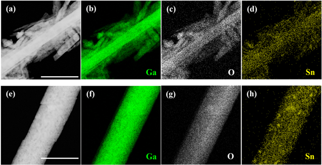
Figure 2. (a), (e) TEM and (b)–(d), (f)–(h) EDS elemental mapping images of β-Ga2O3 nanostructures with the Sn concentrations of (a)–(d) 0.7 at% (scale bar: 0.7 μm) and (e)–(h) 2.2 at% (scale bar: 0.9 μm). Elemental mappings are marked with different colors for Ga (green), O (grey), and Sn (yellow).
Download figure:
Standard image High-resolution imageThe crystallinities of the β-Ga2O3 nanostructures with different Sn concentrations were characterized using XRD, as shown in Fig. 3a. The X-ray diffraction patterns of the intrinsic β-Ga2O3 nanostructures were indexed to the monoclinic β-Ga2O3. Above the peaks of the monoclinic β-Ga2O3, new peaks corresponding to the (110) and (101) crystallographic planes of SnO2 were clearly observed when the Sn concentration in the β-Ga2O3 nanostructures exceeded 2.2 at%. This also indicated that the Sn concentration of 2.2 at% was beyond the solid solubility limit of the Sn in the β-Ga2O3 nanostructures (consistent with Fig. 2), leading to the precipitation of SnO2. In addition to the SnO2 peaks, several peaks for the SnO (101), (002), and (112) planes were noticeable when the Sn concentration exceeded 2.2 at%. Of note, there were weak shoulders on the peaks representing the (111) and (401) planes of the monoclinic β-Ga2O3, which did not represent Ga2O3, SnO2, or SnO.
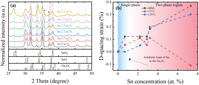
Figure 3. (a) XRD patterns of β-Ga2O3 nanostructures with different Sn concentrations. The bottom tick markings indicate PDF Card No. 00-043-1012 for monoclinic Ga2O3, PDF Card No. 00-041-1445 for tetragonal SnO2, and PDF Card No. 00-001-0891 for tetragonal SnO.
Download figure:
Standard image High-resolution imageIt was also shown that the diffraction peaks representing β-Ga2O3 shifted to a smaller 2θ angle with the Sn concentration, meaning that the substitutional doping of Sn in the intrinsic β-Ga2O3 nanostructures increased the lattice constants of the β-Ga2O3 nanostructures. Figure 3b summarizes the D-spacing strain of the major peaks representing β-Ga2O3 as a function of the Sn concentration in the β-Ga2O3 nanostructures. The D-spacing strain of the (002) and (−311) planes in the β-Ga2O3 continued to increase with the Sn concentration. On the other hand, the inter-plane (111) distance of β-Ga2O3 initially increased and saturated with Sn concentrations. It then decreased at Sn concentration of 3.7 at%, which was presumably affected by the presence of undefined peaks. It was reported that doped-Sn ions were substituted at the octahedral sites of β-Ga2O3. The radii of Sn4+ ions (55 ∼ 81 pm) are comparable to those of Ga3+ (62 pm),24 but the radius of Sn2+ (118 pm) is much larger than that of Ga3+.25
The core-level spectra of the Ga 2p, Sn 3d, and O 1s orbitals of the intrinsic β-Ga2O3 nanostructures are compared with those of Sn-doped β-Ga2O3 nanostructures with different Sn concentrations in Fig. 4. Figure 4a showed that the binding energy (BE) of Ga3+ (Ga2O3) 2p1/2 and 2p3/2 peaks in the intrinsic β-Ga2O3 nanostructures were 1144.8 and 1117.9 eV, respectively, with a peak separation of 26.9 eV. These BE values and the split spin–orbit component for the Ga2O3 were identical to those in the previous results.26,27 Unlike the symmetric peak in the intrinsic β-Ga2O3 nanostructures, the Ga 2p3/2 spectra of the Sn-doped (0.7 at%) β-Ga2O3 nanostructures were asymmetric with a weak shoulder on the main peak at the lower BE. The shoulder peak at 1117.1 eV, with a peak separation of 0.8 eV from Ga3+ (Ga2O3) 2p3/2, continued to increase with the Sn concentration. This indicated that the orbitals of the Ga atoms in the Ga2O3 started to form a chemical bond with the Sn atoms in the β-Ga2O3 nanostructures. In other words, the Sn atoms were introduced into the β-Ga2O3 nanostructures as a substitutional dopant.28 Sn oxidation states were further investigated in Fig. 4b. With the presence of Sn atoms (0.7 at%) in the β-Ga2O3 nanostructures, two components of the Sn 3d line corresponding to the Sn4+ and Sn2+ species with an average peak separation of 0.7 eV were observed.29 Although there are various states in a Sn-O binary system (including SnO2, Sn2O3, Sn3O4, Sn5O6, and SnO), only SnO2 and SnO are known to be thermodynamically stable.30,31 The area of the Sn4+ spectra was larger than that of the Sn2+ spectra, indicating that the formation of SnO2 was preferred to SnO due to the lower Gibbs free energy of formation of SnO2 compared to that of SnO.32 As the Sn concentration increased further, the Sn2+/Sn4+ area ratio continued to increase, indicating that the formation of SnO was also favorable at the higher Sn concentration, as shown in Fig. 4b. The O 1s spectra of Fig. 4c shows that oxygen can be presented in various chemical states such as SnO, SnO2, Ga2O3, and hydroxyl groups (OH–). It is worth noting that the SnO concentration could have been overestimated compared to the SnO2 concentration according to the XPS in this work. In theory, XPS can identify information within 1–10 nm of the surface.33 Based on this theory, on one hand, the SnO presumably remained on the SnO2 surface. On the other hand, the XPS X-ray beam could have transformed the SnO2 into SnO by removing the oxygen ion in the SnO2 even at standard working conditions.34
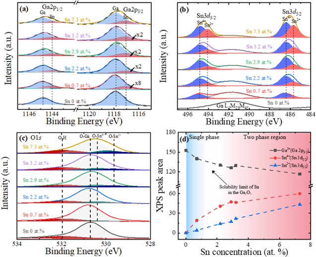
Figure 4. XPS analysis of β-Ga2O3 nanostructures with different Sn concentrations: core-level spectra of (a) Ga 2p, (b) Sn 3d, and (c) O 1s. The subpeak areas of the Sn were enhanced according to the multiplication sign for greater clarity. (d) A comparison of peak areas of Ga3+ (Ga 2p3/2), Sn4+ (Sn 3d5/2), and Sn2+ (Sn 3d5/2).
Download figure:
Standard image High-resolution imageThe optical absorbance and Tauc plots (direct bandgap model) of the β-Ga2O3 nanostructures with different Sn concentrations are compared in Fig. 5a. The optical bandgaps of the Sn-doped β-Ga2O3 nanostructures were obtained using a linear extrapolation of their Tauc plots10 and compared with those of bulk Ga2O3, SnO2, and SnO materials as shown in Fig. 5b. In Fig. 5a, the absorbance of the intrinsic β-Ga2O3 nanostructures was drastically reduced above the wavelength of bandgap energy, which was ascribed to the electron transition from the valence band to the conduction band of the intrinsic β-Ga2O3 nanostructures. This absorption feature was consistent with previous reports.35 The onset of absorption gradually shifted from 280 nm to 380 nm as the Sn concentration increased. The inhomogeneous broadening of the band tail deeply expanded the onset of absorption to 400 nm, which was caused by the Sn dopants in the β-Ga2O3 nanostructures. This broad absorption tail was attributed to the electronic transition from the valence band of β-Ga2O3 nanostructures to the energy level of Sn dopants serving as the electron acceptors. The effect of cationic doping has been known to reduce the optical bandgap energy, shifting the light absorption range closer to the visible range in the β-Ga2O3 nanostructures.36,37 Figure 5b reveals that the optical bandgap energy of the Sn-doped β-Ga2O3 nanostructures decreased from about 4.8 to 4.1 eV with increasing Sn doping concentration (from 0 to 7.3 at%). This optical bandgap reduction for the Sn concentration was also consistent with the theoretical calculation using the first-principles based on density function theory.37
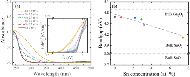
Figure 5. (a) Optical absorbance spectra and Tauc plots (direct bandgap model) and (b) corresponding optical bandgap of the β-Ga2O3 nanostructures with different Sn concentrations, which was compared with that of SnO2 and SnO. The bandgaps of the Ga2O3, SnO2, and SnO were derived from,20,38 and,39 respectively.
Download figure:
Standard image High-resolution imageFigure 6 shows the absorbance spectra of the MB solutions and photocatalytic activity of β-Ga2O3 nanostructures with different Sn concentrations. The photocatalytic activity value of the intrinsic β-Ga2O3 nanostructures was around 40% from Eq. 1 (see the experimental section). This value increased significantly to as high as 90% with the addition of a small amount of Sn (0.7 at%) in the β-Ga2O3 nanostructures. However, when the Sn concentration further increased, the photocatalytic activity value continued to decrease with the Sn concentration in a range from 0.7 to 3.2 at%, and the value flattened out until a Sn concentration of 7.3 at%.
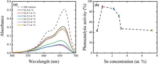
Figure 6. (a) Absorbance spectra of the MB solution and (b) photocatalytic activity in the presence of β-Ga2O3 nanostructures with different Sn concentrations under UVC irradiation for 20 min at room temperature. The error bars in the photocatalytic performance are graphical representations of a standard deviation of three-time measurements.
Download figure:
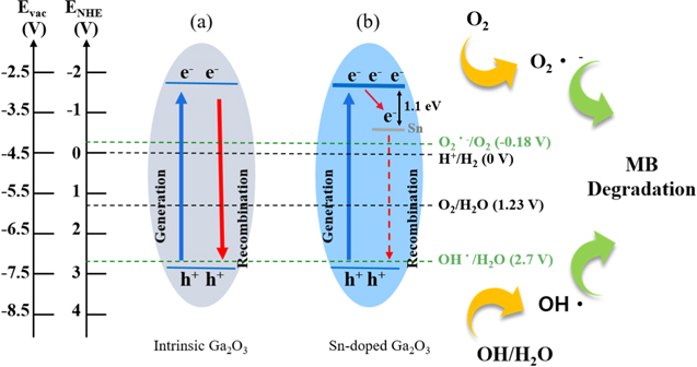
Standard image High-resolution imageThe photocatalytic activities of the β-Ga2O3 nanostructures at different Sn concentrations can be correlated with the results obtained from the XRD (Fig. 3) and XPS (Fig. 4), and also explained using the schematic diagram shown in Fig. 7. Figure 7a shows that the generation of both the OH and O2 radical was thermodynamically favorable upon the photoexcitation of the intrinsic β-Ga2O3 nanostructures. In other words, the photogenerated electrons in the conduction band at −1.5 eV (vs normal hydrogen electrode (NHE)) produced superoxide radicals (O2·−) via a reduction of ambient oxygen (O2), and the photogenerated holes in the valence band at 2.8 eV (vs NHE) produced hydroxyl radicals (OH·) either directly via the oxidation of H2O or indirectly from superoxide radicals (O2·−).16,40,41 Those produced radicals have been considered as the most active species for MB degradation.21,41,42 The photocatalytic efficiency was affected by the carrier dynamics of the generated charges in a catalyst: generation, trapping, and interfacial transfer, as well as the recombination of charge carriers.36,43–45 Prior to photocatalytic redox reactions, generated electrons and holes can be readily recombined at the surface or in the bulk of the catalyst with the energy release to photons or phonons,43 which degrades photocatalytic efficiency. Thus, the photocatalytic activity can be enhanced by improving the electron and hole separation. Figure 6b shows that the electron trap sites in the Sn-doped (0.7 at%) β-Ga2O3 nanostructures enhanced the photocatalytic activity to as high as 90% compared to the intrinsic β-Ga2O3 nanostructures. As the Sn concentration continued to increase, the photocatalytic activity started to decrease with the Sn concentration in a range of 0.7 to 3.2 at%, and the value flattened out until the Sn concentration of 7.3 at%, which was attributed to the precipitated Sn oxides along with the Sn-doped β-Ga2O3 nanostructures, as evidenced from the EDS (Fig. 2), XRD (Fig. 3), and XPS (Fig. 4). The presence of Sn oxides could have reduced the quantum yield of the Sn-doped (0.7 at%) β-Ga2O3 nanostructures by absorbing or scattering UVC light and eventually limiting the absorption capacity of the Sn-doped (0.7 at%) β-Ga2O3 nanostructures due to the shielding effect. In addition, the lattice distortion of the β-Ga2O3 nanostructures with Sn concentration, as shown in Fig. 3b, in part, degraded the photocatalytic activity by providing electron and hole recombination centers.46,47
Figure 7. Schematic illustration of charge transfer mechanism under UVC irradiation in (a) intrinsic β-Ga2O3 nanostructures, (b) Sn-doped (0.7 at% under the solid solubility limit in Ga2O3) β-Ga2O3 nanostructures. The defect state caused by the Sn doping was 1.1 eV below the conduction band of the Ga2O3.48 The OH radicals can be generated via two routes in photocatalysis—either directly from a redox potential of 2.8 V (vs NHE) or indirectly from intermediate radical O2 at a redox potential of −0.2 V (vs NHE).49
Download figure:
Standard image High-resolution image
Conclusions
Sn-doped β-Ga2O3 nanostructures with different Sn concentrations were synthesized using a hydrothermal method, and their photocatalytic properties were evaluated using MB degradation under 254 nm irradiation. The photocatalytic activity of the Sn-doped (0.7 at%) β-Ga2O3 nanostructures increased significantly compared to that of the intrinsic β-Ga2O3 nanostructures. The Sn trap sites in the forbidden bandgap of the Sn-doped β-Ga2O3 improved the charge separation and thereby enhanced the photocatalytic activity. On the other hand, as the Sn concentration continued to increase, the photocatalytic activity started to decrease with the Sn concentration in the range of 0.7 to 3.2 at%, and the value flattened out until the Sn concentration of 7.3 at%, which was attributed to the precipitated Sn oxides along with the Sn-doped β-Ga2O3 nanostructures. The presence of the SnO and SnO2 degraded the overall photocatalytic efficiency in the β-Ga2O3 nanostructures.
Acknowledgments
This work was funded by the National Research Foundation of Korea (NRF) through the Basic Science Research Program (2017R1A2B4012278), and by the Center for Advanced Soft-Electronics funded by the Ministry of Science, ICT and Future Planning, through the Global Frontier Project (CASE-2011-0031638). The SEM/EDS and XRD analyses were conducted at the Korea Basic Science Institute (Busan Center).