Abstract
The defect structure of HVPE-GaN crystals is examined using synchrotron white-beam X-ray topography (SWXRT) and topography results are interpreted and discussed in comparison to reciprocal lattice point broadening from high resolution X-ray diffraction (HRXRD) measurements. Two as-received commercial HVPE-GaN wafers from two different vendors and one HVPE-GaN which was grown on an ammonothermal GaN-seed are investigated in this study. To our knowledge SWXRT large area back-reflection analysis of HVPE-GaN grown on an ammonothermal GaN seed has been performed for the first time. From large-area topography the formation of a cellular defect network is identified for the commercial HVPE-GaN. Large differences in the crystal lattice misorientation deformation (mosaicity) are determined for the different samples by transmission section topography. For the HVPE-GaN grown on an ammonothermal GaN-seed a very low defect density was ascertained. From the contrasts of the topography threading screw-type dislocations and threading mixed-type dislocations were identified. The X-ray topography analysis shows clearly and for the first time that the nature of the defect structure and the low density of ammonothermal GaN seeds can be transferred by HVPE growth of GaN.
Export citation and abstract BibTeX RIS

This is an open access article distributed under the terms of the Creative Commons Attribution Non-Commercial No Derivatives 4.0 License (CC BY-NC-ND, http://creativecommons.org/licenses/by-nc-nd/4.0/), which permits non-commercial reuse, distribution, and reproduction in any medium, provided the original work is not changed in any way and is properly cited. For permission for commercial reuse, please email: oa@electrochem.org.
For demanding GaN-based (opto-)electronic applications such as laser diodes or transistors for high power electronics there is a need for material with low defect densities, since threading dislocations act as centers of non-radiative recombination, increasing the leakage current, reducing the room temperature mobility and so limiting the efficiency, performance and lifetime of devices. Freestanding GaN with low defect density is the substrate material of choice for the realization of such GaN-based device structures with superior properties. Different approaches for crystal growth of bulk GaN like ammonothermal growth, hydride vapor-phase epitaxy (HVPE) and high- and low-pressure solution growth were followed in recent years.1 The ammonothermal growth and HVPE seem to be the most promising methods to produce GaN substrates in sufficient number, size and material quality and substrates prepared with these growth methods have become available commercially in recent years. In the ammonothermal growth method, GaN crystalizes from a solution of Ga in supercritical ammonia with the addition of a mineralizer. For seed material, the ammonothermal growth method uses native GaN crystals. Benefits of the ammonothermal growth method are very low dislocation densities as low as 5 × 103 cm−2 and large curvature radii of the crystal planes (>100 m).2 Drawbacks of GaN ammonothermal growth method are the incorporation of impurities and the low growth rate (0.1 mm/day), even when the method can potentially produce hundreds of crystals in a single batch. In comparison, in HVPE the GaN crystallization takes place from the vapor phase by the reaction of ammonia with gallium chloride at temperatures of about 1050°C. HVPE uses GaN seed layers (templates) deposited e.g. by metal-organic vapor phase epitaxy on foreign substrates (typically sapphire or GaAs). After growth the thick quasi bulk GaN layer has to be separated from the foreign substrate. Advantages of the HVPE method are the high purity of the crystals and a high growth rate (>100 μm/h). As a consequence of the lattice mismatch and different thermal expansion between GaN and the foreign substrate a relatively high density of threading dislocations (106–107 cm−2) and large wafer curvature are typically observed. The high dislocation density of HVPE-GaN crystals is not a principal disadvantage of this growth process, but is based on the use of foreign substrates with large lattice mismatch and different thermal expansion.3 Sochacki et al. have shown that low dislocation density ammonothermally grown GaN crystals can be successfully used as seeds for the HVPE growth and it is possible to combine the benefits of both growth methods, ammonothermal growth method and HVPE, and crystallize low dislocation density GaN crystals.4,5 The lattice parameter of the ammonothermal GaN-seed material and the grown HVPE-GaN crystals had the same values within the experimental error (a = 318.97 ± 0.02 pm and c = 518.51 ± 0.01 pm) showing that no stress was introduced. Moreover the HRXRD 0002 rocking-curve full widths at half maximum (FWHM) of the HVPE crystals of approximately 40 arcsec were in the same order of magnitude as the ammonothermal seed material.4
Depending on the type of growth method, but also within the same growth method, significant differences in the defect structure of the GaN substrates can be observed in samples obtained from different manufacturers. Information about the structural quality of GaN substrates given by the manufacturers are often limited to e.g. rocking curve FWHM, which reveal few details on the defect structure of the material. For industry and other institutions that deal with the development of GaN-based power devices, there is a lack of information about the structural properties of commercially available GaN substrates which is necessary for device development. On the other hand, with decreasing dislocation density detailed defect analysis is becoming increasingly difficult as methods such as transmission electron microscopy (TEM) are limited or only possible with considerable effort. A particular advantage of X-ray topography is its ability to cover large mm2 areas at micron resolutions. TEM techniques, albeit providing resolutions on the order of nanometers, cannot cover large areas of substrates, which is a pre-requisite for wafer scale substrate analysis.
Synchrotron white-beam X-ray topography (SWXRT) is an established technique for the analysis of defects / dislocations in bulk crystals with low dislocation density (∼105 cm−2 and below). The method is very sensitive to crystal misorientation and microstrain. In a simplified view, misorientations within a crystal, e.g. subgrains in a mosaic crystal, become visible as an orientation contrast resulting from inhomogenous intensity distributions originating from diffracted X-ray with varying directions. Likewise, a distortion of crystal planes δd will change the Bragg angle Θ. As any dislocation induces microstrain, the dislocation becomes visible as a contrast variation in the topography. A more comprehensive description of contrast mechanisms in X-ray topography can be found elsewhere.6 So far, X-ray topography techniques have been rarely used for the characterization of GaN crystals in the past. This is certainly due to the often high dislocation density of GaN crystals. On the other hand the work of, for example Chen et al., shows that techniques such as SWXRT transmission section topography are quite suitable to gain information on the crystal quality of GaN with high dislocation density.7
In this work we present a detailed analysis of defect structures of commercially freestanding GaN (0001) crystals grown by HVPE and a HVPE-GaN sample grown on an ammonothermal GaN-seed. The ammonothermal GaN-seed was provided by Ammono S.A., Warsaw, Poland. Synchrotron white-beam X-ray topography (SWXRT) and high resolution X-ray diffraction (HRXRD) were used for this combined study. SWXRT in two principal X-ray topography geometries was used in the course of this analysis, namely the large-area back-reflection mode and section transmission mode. HRXRD reciprocal space mappings and in-plane measurements were used for mosaicity analyses. The combination of these methods allows a detailed statement of the nature, density and distribution of typical defects in GaN bulk crystals with a large field of view.
In this study we are interested examining significant differences in the defect structure of the GaN substrates which can be observed in samples obtained from different manufacturers or as a function of the growth technique. While this work does not represent a comprehensive survey of the plurality of commercially available substrates, the aim of this work is to examine the impact of the variability of different substrate types in order to verify the actual crystalline quality of the materials, rather than those claimed in datasheets or vendor brochures. This work is not without precedent as previous work on SiC substrates confirmed an alarming variability in actual substrate defectivity, which was often at odds with manufacturer/vendors claims.8
Experimental
For this study we used two as-received commercially freestanding GaN substrates grown by HVPE from two different vendors (referred to as sample H-1 and sample H-2). Details of the growth conditions of the commercial substrates are not known. The samples have nominally a chemo-mechanical polishing (CMP) with a roughness of < 0.5 nm and the nominal dislocation density is specified by the manufacturers as 3 × 107 cm−2 for sample H-1 and 5 × 106 cm−2 for sample H-2. A third sample for this study is a non-commercially HVPE-GaN sample grown on an ammonothermal GaN-seed (referred to as sample H-A). The details of the growth conditions for sample H-A are given in Ref. 5. After HVPE growth the ammonothermal GaN-seed was cut off from the sample, leaving only the HVPE part for the structural investigations. All samples have a (0001), c-plane orientation and the structural investigations were performed on the Ga-face side. Information about the size and the thickness of the samples are given in Table I.
Table I. Size and thickness of investigated samples.
| Sample | Size | Thickness |
|---|---|---|
| H-1 | 50 mm diameter wafer | 260 μm |
| H-2 | 10 mm × 10 mm wafer | 261 μm |
| H-A | Half of 25 mm diameter wafer | 310 μm |
Synchrotron white-beam X-ray topography (SWXRT) was performed at the TOPO-TOMO beamline at the ANKA synchrotron light source at the Karlsruher Institute of Technology (KIT), Karlsruhe, Germany, utilizing the continuous spectrum (white light) of synchrotron radiation from bending magnet of the 2.5 GeV storage ring and beam currents of 180 – 80 mA. No optical components between the bending magnet source and the experimental station were used in the beamline, except for one Be-window directly in front of the experiment. A double slit system inside the vacuum tube controlled the irradiated area of the sample. The 30 m long source-to-sample distance and the small source size of 800 μm × 200 μm (horizontal × vertical) resulted in a high geometrical resolution of the topographs of about 1 μm. Further details of the beam line characteristics at the ANKA synchrotron light source can be found elsewhere.9 For the measurements the samples were mounted on a 2-circle goniometer with x- and z-translation.
For the topography the samples were placed into the white X-ray beam. The principle of white-beam X-ray topography is basically analogous to the Laue method: The lattice planes (hkl) of a single crystal select out of the continuous spectrum the matching wavelengths λ and achieve the diffraction condition, according to Bragg's law:
![Equation ([1])](https://content.cld.iop.org/journals/2162-8777/4/8/P324/revision1/jss_4_8_P324eqn1.jpg)
where dhkl is the inter-planar spacing of the lattice planes (hkl), ΘB is the Bragg angle, λ is the wavelength of the diffracted beam. Therefore every diffraction vector  which fulfills Bragg's law, results in one topograph from the same illuminated part of the sample during one single exposure arising in a Laue pattern of topographs.
For X-ray topography in this study the large-area back-reflection and section transmission geometry were used. In the large-area back-reflection geometry the X-ray beam size was 4.0 mm × 4.0 mm. A sample-to-film distance of 98 mm was used and the sample was tilted 7° about the horizontal axis. The topographs were recorded on SLAVICH VRP-M high resolution films (grain size: 0.05 μm) with exposure times of 120 – 240 s. For the section transmission geometry the X-ray beam size was 10 mm in horizontal direction and limited in the vertical direction to 15 μm. Here, a sample-to-film distance of 87 mm was used and a sample tilt of 12° about the horizontal axis. For the measurements in this geometry AGFA D3sc films were used with exposure times of 90–150 s. The software LauePT was used for the orientation of the crystals and indexing of the Laue pattern.10 Fig. 1 shows an example of an exposure of the white beam transmission section topography. The indexed reflections were used for evaluation.

Figure 1. Example of an exposure of the white beam transmission section topography. The indexed reflections were used for evaluation.
Additional to the SWXRT measurements, laboratory high resolution X-ray diffraction (HRXRD) measurements were performed with a PANALYTICAL X'pert Pro Materials Research Diffractometer. The system was equipped with a parabolically bent graded multilayer mirror and a 4 × Ge 220 monochromator providing Cu-Kα1-radiation (λ = 154.059 pm) at the primary beam side and a 3 × Ge 220 analyzer before the detector. The used X-ray beam had a width of 1 mm and a height of 5 mm. Reciprocal space mapping (RSM) of the 0002, 0004, 0006 and  GaN reflections were accomplished for the analysis of the mosaic tilt of the GaN wafers. The mosaic twist was measured by in-plane ω-scans of the
  GaN reflection and for comparison purposes ω-scans of 0002 GaN reflections.
Results
Large-area back-reflection topography of HVPE-GaN on foreign substrate
Fig. 2 and 3 show the 0006 and  GaN large-area back-reflection topographs of both commercial HVPE-GaN samples H-1 and H-2, respectively. The exposures reveal a blurred light-dark contrast with a mosaic-like grain structure. This contrast on the topographs can be interpreted as orientation contrast of heavily deformed crystal with tilted and twisted GaN grains. Due to the lattice misorientation, the diffracted beams can overlap or diverge, indicating a mosaic structure of independently diffracting cells.6 Particularly conspicuous is that on the topographs of sample H-1 the individual grains are separated by dark contrast of relatively sharp line structures. An interpretation of these line structures as individual dislocations would be obvious but this assumption cannot be sustained on a closer analysis: A simple proof whether these line contrasts are due to dislocations would be by the implementation of a standard Burgers vector analysis. In such an analysis, the contrast change of dislocations from different Laue reflections measured at the same sample region can be analyzed as long as single dislocations can be resolved. For the case that the contrast of individual dislocations disappears in certain reflections, the type and direction of the dislocation can be determined by using the b · g = 0 criterion for the contrast extinction of screw-type dislocations, and the combined criterion b · g = 0 and g · b × l = 0 for the contrast extinction of edge- or mixed-type dislocations (with g = diffraction vector, b = Burgers vector and l = dislocation line direction).6 For the hexagonal GaN the Burgers vector of an elemental threading screw dislocation is bscrew= [0001], threading edge dislocation
  and threading mixed dislocation
  . Such a classical Burgers vector analysis was not possible in the case of sample H-1 and H-2 because of the high dislocation density. HVPE-GaN grown on foreign substrate has a typical dislocation density in the range of 106 cm−2 – 107 cm−2. But nevertheless the above mentioned Burgers vectors had to be expected in our crystals, too. This density is too high, since the detectability limit for individual dislocations using SWXRT technique is in the order of 104 cm−2 – 105 cm−2.11 A more plausible explanation for these sharp lines of contrasts of sample H-1 is that we observe the strain fields of a cellular dislocation network. The sharp line-features are convoluted contrasts caused by bundles of more or less parallel but snakelike tangled dislocations. The dislocations tend to be concentrated in and around the cellular walls with central regions tending to have less dislocation density. As a rough estimate, the average cell diameter is about 100 μm. For sample H-2 (Fig. 3) these sharp lines contrasts on the topographs are not as pronounced compared to sample H-1. In addition, the whole general contrast variation for this sample seems to be less distinctive, both suggesting a lower dislocation density. The size of the grains estimated from the large-area back-reflection topographs for sample H-2 is of comparable magnitude (∼ 100 μm) as for sample H-1.
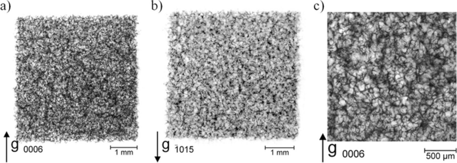
Figure 2. Large-area SWXRT recorded from sample H-1, a) 0006 reflection, b)  reflection and c) enlargement of 0006 reflection.
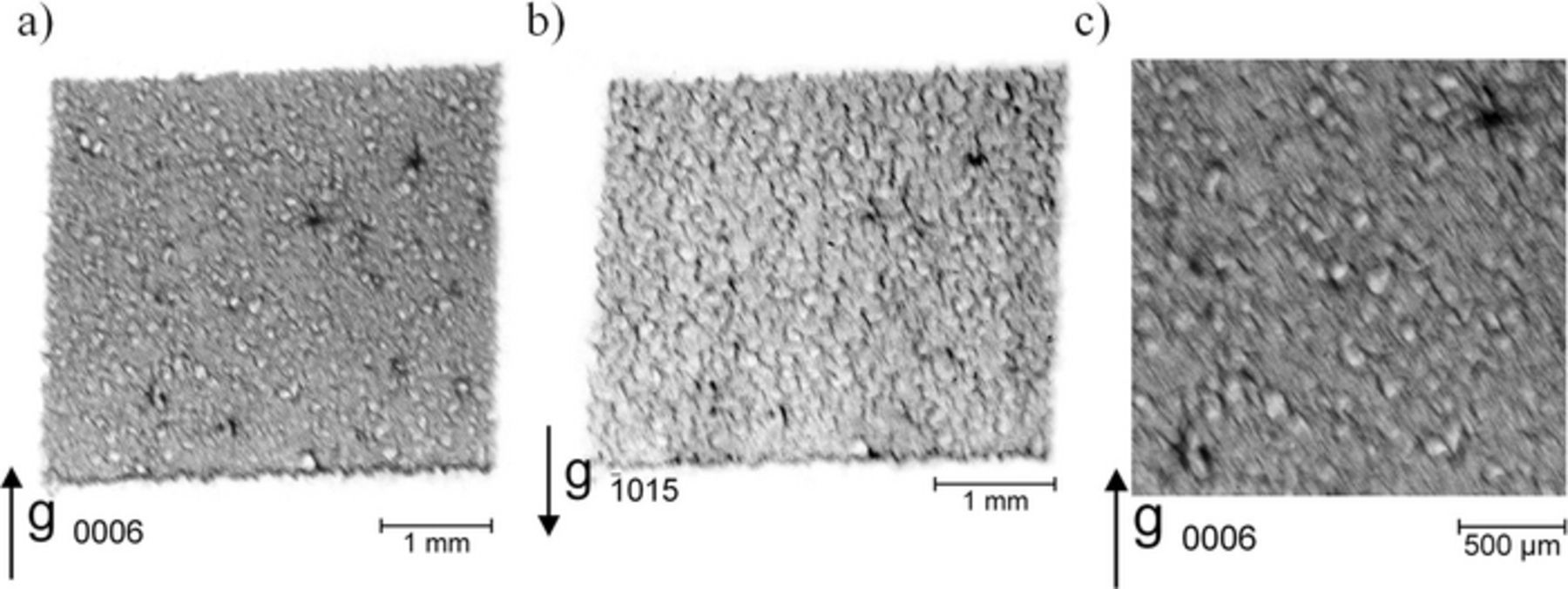
Figure 3. Large-area SWXRT recorded from sample H-2, a) 0006 reflection, b)  reflection and c) enlargement of 0006 reflection.
Transmission section topography of HVPE-GaN grown on foreign substrate
Clear differences in the micro-structural properties of the two HVPE-GaN wafers can be visualized by the section transmission SWXRT. In this recording geometry the sample's defects again become visible by orientational contrast on a μm-scale. Fig. 4 shows GaN  ,
,  and
and  reflection section transmission topographs taken from the same region of sample H-1. Within the topographs a distribution of features with fuzzy contrast can be observed. No sharp contrasts are visible in this recording geometry compared to the features of relatively sharp contrasts on the large area back-reflection exposures of this sample (Fig. 2). This fuzzy contrast is an indication of the mosaic spread (tilt and twist) of the crystal grains within the GaN material.

Figure 4.  ,
,  and
and  reflection section transmission topographs of sample H-1.
Section transmission topographs,  ,
,  and
and  GaN reflection, of sample H-2 are displayed in Fig. 5. On the topographs, images of severely distorted areas which are effectively shifted to different locations of the exposures with respect to the adjacent better matrix material are recorded. Enlarged images of the contrasts in Fig. 5A and 5B are representing the extremities of completely cracked regions and in Fig. 5C small angle grain boundaries are resolved whose edges are delineated. The distance between small angle grain boundaries are in the range of 70 – 140 μm. Another feature that becomes visible by the bending of the section recording is the curvature of the wafer, as indicated by the dashed line for the
  reflection. From HRXRD curvature measurement a mean curvature radius of about – 4 m was determined.
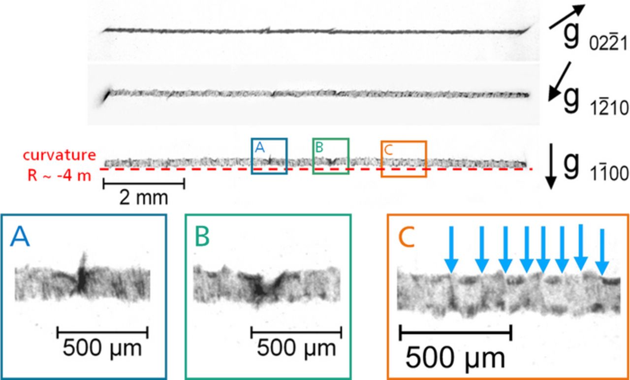
Figure 5.  ,
,  and
and  reflection section transmission topographs of sample H-2. In A and B cracked regions are visible and in C small angle grain boundaries are resolved. The arrows in C mark the small angle grain boundaries.
It is striking that the contrasts in the section topography of sample H-1 are significantly more fuzzy and broadened compared to sample H-2. If one had a perfect crystalline sample, to a first approximation, the section topographic slice would essentially be the projected thickness of the sample on the film. However, for these two highly defective HVPE-GaN samples, this is obviously not the case since both samples have a thickness of about 260 μm. Here the X-ray section topographic record is a "pictorial version of rocking curves" across the entire lateral extent, defined by the 10 mm width of the X-ray beam, across the measured sample area. Thus the total effective broadened image is a measure of the maximum extent of the rocking curve broadening due to crystal mosaicity for every location across the measuring spot of the sample. Chen et al. used SWXRT section transmission topography for the quantitative determination of maximum crystal misorientations ΔΘmax of lateral epitaxial overgrown GaN on sapphire substrate.7 We adapted this evaluation method for the quantitative determination of maximum crystal misorientations ΔΘmax for thick freestanding HVPE-GaN material. Following this approach, the width Δw of the fuzzy contrast provides quantitative information about the GaN crystal lattice misorientation deformation. The maximum extent of crystal lattice misorientation deformation ΔΘmax can be extracted by the relation:
![Equation ([2])](https://content.cld.iop.org/journals/2162-8777/4/8/P324/revision1/jss_4_8_P324eqn2.jpg)
with Θ being the Bragg angle and L is the distance from the center of the transmitted beam to one Laue spot. L can be calculated using the distance from the film to the sample D by the formula:
![Equation ([3])](https://content.cld.iop.org/journals/2162-8777/4/8/P324/revision1/jss_4_8_P324eqn3.jpg)
Figure 6 shows the approach for determining the maximum crystal lattice misorientation deformations ΔΘmax for sample H-1 and H-2 from SWXRT section transmission topography for the  GaN reflections. The application of this evaluation results in a maximum crystal lattice misorientation deformation ΔΘmax of 846.0 arcsec calculated from a Δw of 0.86 mm for sample H-1. The sample H-2 yields a maximum crystal lattice misorientation deformation ΔΘmax of 295.2 arcsec determined from a Δw of 0.30 mm.
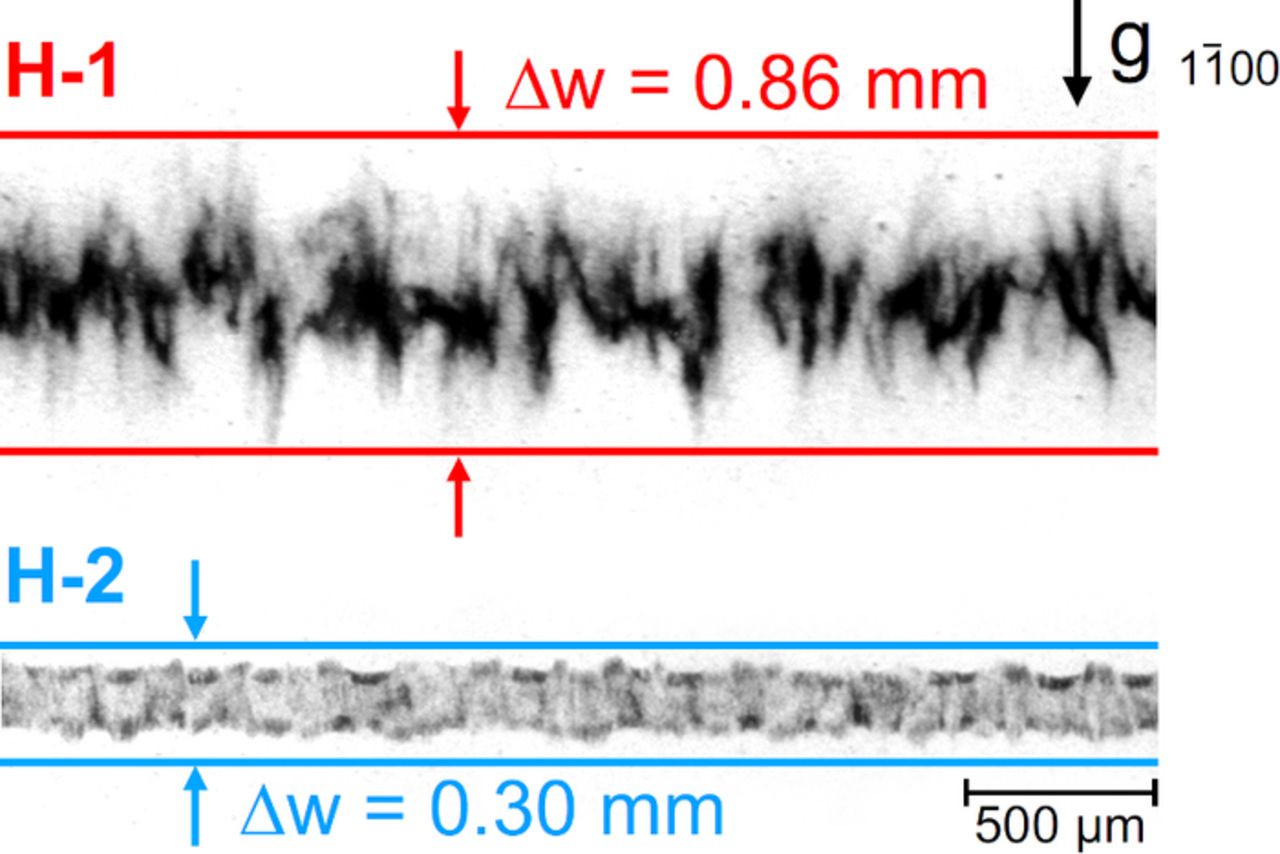
Figure 6.  reflection section transmission topographs of sample H-1 and H-2 used for the evaluation of the maximum crystal lattice misorientation deformations ΔΘmax.
Large-area back-reflection topography of HVPE-GaN grown on an ammonothermal GaN-seed
The SWXRT topography of the investigated HVPE-GaN grown on an low defect density ammonothermal GaN-seed (sample H-A) shows a significantly different defect structure compared to the HVPE GaN material grown on a foreign seed material like sample H-1 and H-2. At first sight a uniform gray contrast is visible on the SWXRT large-area back-reflection topographs, indicating a high degree of structural quality. Fig. 7a shows as an example the  reflection topography of sample H-A. On closer contemplation predominantly white contrasts are visible.
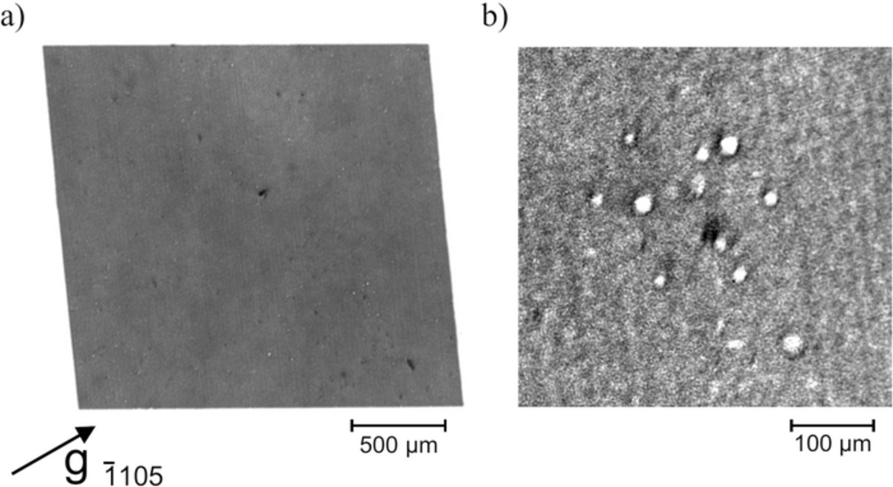
Figure 7.  reflection large-area SWXRT recorded from sample H-A, b) shows individual screw dislocations.
These contrasts are related to threading screw-type dislocations (TSD) and threading mixed-type dislocations (TMD). This was determined from a dislocation analysis using invisibility criteria from 0006 and  reflection topographs. No pure edge-type dislocations were identified which should have become visible in the asymmetric
  reflection topography and invisible in the symmetric 0006 topography. These results are in good agreement with recently published SWXRT studies of Sintonen et al. for (unblended) ammonothermally grown GaN crystals.12,13 In that work it was shown by comparison of measured and simulated SWXRT images that TSDs appear as symmetric white area with a dark circumference, while the TMDs have asymmetric black to white contrast with six different distinct contrast directions. Moreover, the TSDs are observed in a few discrete sizes. The symmetric white rings with the smallest diameter are caused by a single TSD, and features with a larger diameter are caused by overlapping strain fields of adjacent TSDs. Only discrete white circle sizes are possible, since the strain fields are directly proportional to integer multiples of the screw dislocation Burgers vector magnitude b = n · c, where n is an integer, and c is the out-of plane lattice parameter.12 Similar features are well known from SWXRT images of super-screw and hollow-core screw dislocations (micropipes) in SiC.14,15 This kind of TSDs are also present here for the investigated HVPE-GaN crystal grown on an ammonothermal GaN-seed. The Fig. 7b shows an enlarged image of the
  reflection topography with several TSDs. The typical symmetric white ring contrasts with dark circumference are visible. For the contrast features of these dislocations two different discrete circle sizes are found with diameters of approximately 15.0 μm and 18.5 μm. This indicates that at least for the larger diameter contrasts, groups of adjacent TSDs are involved with overlapping strain fields. The density of the TSDs is determined to ∼ 1 × 104 cm−2. Despite the defects found, the topographs of sample H-A give no signs of a pronounced mosaic structure as was observed for sample H-1 and H-2 showing that the high structural quality of the ammonothermally grown GaN-seed is adopted by the HVPE grown GaN. Regarding the results of this work as well as the work of Sintonen et al., there is a controversy with the literature.12,13 Sochacki et al. reported the existence of threading edge dislocations (TEDs) in both, ammonothermal GaN and HVPE-GaN grown on ammonothermal GaN-seeds, as determined from defect selective etching.16 This controversy has to be elucidated in further studies.
High resolution X-ray diffraction
Differences concerning the defect structure of the three samples become also evident in the HRXRD measurements using reciprocal space mapping (RSM) and ω-scans. The Fig. 8 shows the RSMs of the 0002, 0004, 0006 and  GaN reflections of sample H-1, H-2 and H-A. A large amount of mosaic tilt is detected in the RSMs of sample H-1 (Fig. 8a). This is displayed in a large smearing out of the reciprocal lattice points in q// -direction. For sample H-2 (Fig. 8b) this broadening is less pronounced indicating a lower tilt and the RSMs of sample H-A show the fewest features for tilt (Fig. 8c). These HRXRD results are in good agreement with the results from SWXRT. In the section transmission topographs of sample H-1 a large smearing out of the contrast due to crystal misorientations was observed while sample H-2 showed better oriented material. Interesting observations can be made from the full width at half maximum (FWHM) values of the GaN 0002 ω-scans (Fig. 9a). HRXRD ω-scans of GaN 0002 reflection are commonly used to receive information about the mosaic tilt. The FWHM from a Gaussian fit of the 0002 reflections reveals for sample H-1 with 177.9 arcsec a lower broadening than the same reflection of sample H-2 with a FWHM of 209.1 arcsec. This would indicate that sample H-1 has a smaller tilt compared to sample H-2. On the other side, if one considers the flanks of the 0002 reflections, it can be ascertained that the flanks of the reflection of sample H-2 are steep compared to those of sample H-1. Comparing the RSMs of the two crystals the RSMs of sample H-1 resemble the RSM pattern of thin GaN films with typically high mosaicity and very small crystal grains, while the RSMs of sample H-2 equal a proper (mosaic) bulk crystal. The larger FWHM for the 0002 reflection of sample H-2 can be explained by the superposition of diffraction maxima from several large subgrains of the GaN crystal. This is also evident from the asymmetry and the splitting of the ω-scan 0002 reflection. The in-plane ω-scans of the GaN
  reflections, however, clearly show that the sample H-1 has a significantly larger twist component. With a value of 392.4 arcsec the FWHM of sample H-1 for the
  reflection is more than five times larger than the FWHM of sample H-2 having a value of 77.0 arcsec. Including into this analysis the values for the maximum extent of crystal lattice misorientation deformation ΔΘmax, determined from the transmission section topographs, this clearly confirms the trend that sample H-1 has a larger mosaicity. Comparing the numbers of maximum crystal lattice misorientation deformations ΔΘmax and the FWHMs of the 0002 ω-scans, we find fair agreement for sample H-2, ΔΘmax = 295.2 arcsec and FWHM = 209.1 arcsec. This match cannot be found for sample H-1 having values of ΔΘmax = 846.0 arcsec and FWHM = 177.9 arcsec. As discussed above in connection with RSMs of sample H-1, the number for the FWHM seems to be less reliable. This is confirmed by the results of the maximum crystal lattice misorientation deformation analysis from SWXRT and an interpretation of the HRXRD reflection broadening must be performed using reasonable care, since these results are otherwise deceptive.
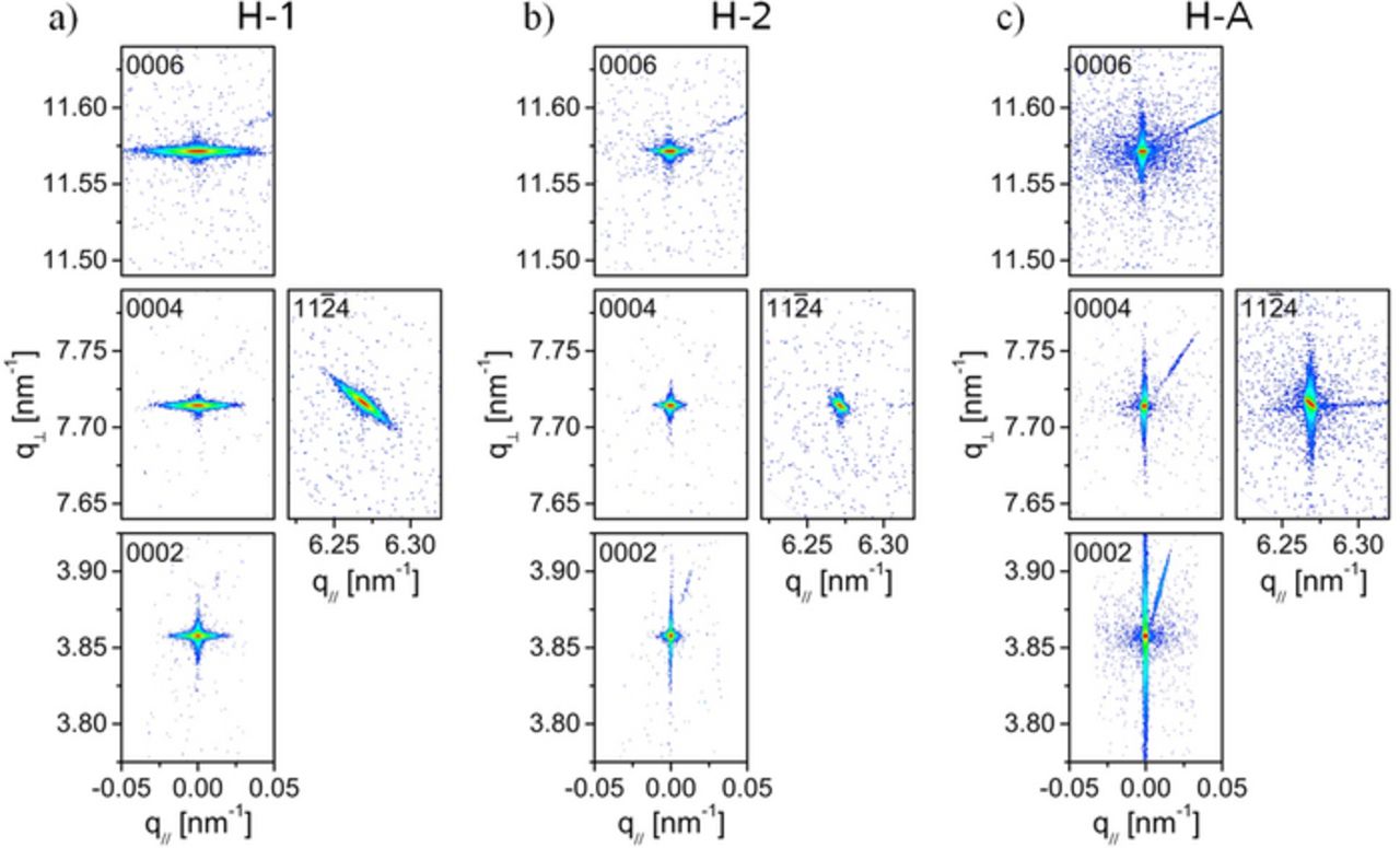
Figure 8. HRXRD 0002, 0004, 0006 and  GaN reflection reciprocal space mappings (RSMs) of a) sample H-1, b) sample H-2 and c) sample A-H.

Figure 9. HRXRD GaN 0002 and in-plane  reflection ω-scans. The measurement curves of the 0002 reflections are shown shifted on the intensity axis for clarification.
The much better material quality of sample H-A, as determined from the topography, is also reflected in the HRXRD measurements. For the measurements of the RSMs one can observe only a very small broadening of the reciprocal lattice points with increasing diffraction order (Fig 8c). This indicates low tilt content for that sample. The GaN ω-scan 0002 scan shows the smallest FWHM of all investigated samples from this study (Fig. 9a) of 116.0 arcsec. The flanks of the reflection are very steep, nevertheless the reflection has a slight asymmetry and a small shoulder on the left side. For the in-plane GaN  ω-scan a FWHM of 12.9 arcsec was determined (Fig. 9b). The low FWHMs of the ω-profiles, with a larger value for the 0002 reflection and a very small value for the
  reflection are in good agreement with the results from topography. In the topographs TSDs and TMDs were detected. TEDs could not be observed and their density seems to be therefore low. The TSDs and the screw component of the TMDs affect the mosaic tilt and can be detected in a broadening of the omega profile of e.g. the GaN 0002 reflection. In comparison, TEDs and the edge component of the TMDs influence the mosaic twist. Twist can be detected by the broadening of the omega profile of e.g. GaN
  reflection.
Interesting features which become visible in the RSMs of sample H-A (Fig. 8b) are crystal truncation rods (CTRs). CTRs are dynamical X-ray scattering effects that appear as continuous rods of intensity connecting Bragg peaks along the direction of the surface normal. In reciprocal space, the CTRs become visible as broadened streaks in q⊥-direction and become apparent from the loss of translational invariance and the crystal lattice order in the near surface region. Therefore, the presence of the CTRs indicates a good surface preparation.17,18The RSMs of the samples H-1 and H-2 also show this effect (Fig. 8a, 8b), however, the CTRs are less pronounced and mainly visible only in the RSMs of the 0002 reflections.
Discussion and Conclusions
It is shown that SWXRT is a useful and also non-destructive analytical technique which is ideal for defect analysis of GaN crystals. Section topography is especially suitable to analyze crystal misorientation effects for GaN with high dislocation density in the range of up to 107 cm−2. In detail, for two commercial samples, H-1 and H-2, the formation of a cellular dislocation network for HVPE-GaN was observed by SWXRT and compared to the HRXRD method. This cellular dislocation network was very distinctive for sample H-1. Similar dislocation networks have been observed in other semiconductor bulk and thin film materials (e.g. GaAs, GaP, SiC, CdTe), metals, metallic alloys and dielectric crystals.19,20 The dislocation rearrangement into cell networks takes place under external or internal stress in the course of plastic relaxation. In growing crystals cellular structures are formed due to the acting of the internal thermomechanical stress field.19 Basically, the convergence of dislocations is an energy minimization process. The stress fields overlap and there is a gain of energy for the cellular wall formations (screening effect). For devices fabricated on substrates the cellular structures can cause problems because of the associated electrical inhomogeneities. Weyher et al. have already demonstrated the formation of a cellular dislocation networks for HVPE-GaN using selective etching.21 Our work shows that concerning the misorientations of the individual mosaic crystal grains large differences can occur, which can be discovered by SWXRT because of its wide field of view and sensitivity to even small tilt angles. Unfortunately, the present samples H-1 and H-2 are from a commercial source and feedback concerning the growth conditions was not possible.
For the investigated HVPE-GaN grown on low defect density ammonothermal GaN-seed (sample H-A) an extremely good GaN crystal quality was ascertaind by SWXRT and HRXRD. The comparison of this work with the results of the defect analysis of ammonothermal GaN crystals by Sintonen et al. shows that for this HVPE-GaN an analogous defect structure has formed.12,13 The dislocations identified are TSDs and TMDs. The consequences of these defects, particularly of the TSDs, on the properties for e.g. high-power electronics, such as Heterojunction Bipolar Transistors (HBTs) need to be pursued. Single and groups of TSDs might act as sources for breakdown degradation in GaN-based high-power electronic devices as was observed for SiC.22 From the viewpoint of crystal growth, these X-ray analyses show that the HVPE growth method has the potential to produce low-dislocation GaN crystals with dislocation densities in the range of ∼104 cm−2 and below. A prerequisite for this are GaN-seed crystals with correspondingly low defect density as the ammonothermal GaN material used here.
Acknowledgments
The Synchrotron Light Source ANKA of Karlsruhe Institute of Technology (KIT), TopoTomo beamline, is acknowledged for provision of topography instruments and we thank T. Müller and H. Schade for excellent assistance. We thank P. Rudolph, Berlin, for valuable discussions concerning the formation of cellular dislocation networks in our samples. The research leading to these results has received funding from the European Community's Seventh Framework Programme (FP7/2007-2013) CALIPSO under grant agreement nº 312284.