Abstract
A good candidate for replacing the inert platinum (Pt) electrode in the well-behaved Cu/TaOx/Pt resistive RAM memory cell is ruthenium (Ru), already successfully deployed in the CMOS back end of line. We benchmark Cu/TaOx/Ru device against Cu/TaOx/Pt and investigate the impact of embedment of Cu/TaOx/Ru on two different substrates, Ti(20nm)/SiO2(730nm)/Si and Ti(20nm)/TaOx(30nm)/SiO2(730nm)/Si, on the cell's electrical performance. While the devices show similar switching performance at some operating conditions, there are notable differences at other operation regimes shedding light on the basic switching mechanisms and the role of the inert electrode. The critical switching voltages are significantly higher for Ru than for Pt devices and can be partly explained by the work function difference and different surface roughness of the inert electrode. The poorer switching properties of the Ru device are attributed to the degraded inertness properties of the Ru electrode as a stopping barrier for Cu+ ions as compared to the Pt electrode. However, some of the degraded electrical properties of the Ru devices can be mitigated by an improved integration of the device on the Si wafer. This improvement is attributed to the suppression of crystallization of Ru and its silicidation reactions that take place at elevated local temperatures, present mainly during the reset operation. This hypothesis has been corroborated by extensive XRD studies of multiple layer systems annealed at temperatures between 300K and 1173K.
Export citation and abstract BibTeX RIS

This is an open access article distributed under the terms of the Creative Commons Attribution 4.0 License (CC BY, http://creativecommons.org/licenses/by/4.0/), which permits unrestricted reuse of the work in any medium, provided the original work is properly cited.
The resistive switching (RS) device has recently been of great interest to both industry and academia as a potential replacement for volatile dynamic random access memory (DRAM) and nonvolatile flash technologies that are nearing the end of their dimensional scaling roadmaps.1–9 These two-terminal devices exhibit figure eight-like pinched current–voltage (I–V) hysteresis switching between a high resistance OFF state (Roff) and a low resistance ON-state (Ron) with memristive characteristics.2,3 Resistive switching memory (ReRAM) is classified in subcategories of nanomechanical, magnetoresistive, electrochemical, valence change, thermochemical, and phase change memory.7 The focus of this work is on the electrochemical and valance change filamentary (also called conductive bridge or CBRAM) memory. In particular, Conductive Bridging Random Access Memory (CBRAM), also referred as Programmable Metallization Cell (PMC), is a promising candidate for a resistive memory device due to its highly scalable and low-cost technology.10 CBRAM memory is being extensively explored as a promising candidate for a resistive memory device.11 Both types of resistive switching memory have the potential to reduce latency in connectivity constrained computational devices by building resistive switching (RS) memory directly into a CMOS low-k/Cu interconnect to bring memory and logic closer together.12 Large-scale integration of metal-oxide filamentary memory with a selector device based on 1T1R architecture has been reported.13,14 Low-k dielectrics and Cu metal lines prefigure a potential ReRAM cell, and the cross-bar architecture of a typical two-terminal RS device array is essentially the same as a CMOS metal interconnect system. Thus, the interconnect information bottleneck could be untied and morphed into several system architectures using the same device platform.
In general, a CBRAM device consists of an active anode, an insulating layer, and an inert cathode. In some CBRAM devices, the anode consists of Cu, Ag or Ni, which can dissolve, in the insulating layer.15–17 The insulating layer is a solid-state electrolyte, such as SiO2, GeS2, Al2O3, Ta2O5, or TaOx. When a positive voltage is applied to the active electrode, Cu or Ag cations migrate through the solid electrolyte to the inert cathode (Pt or W). The Cu or Ag cations are electrochemically deposited on the cathode to form a nanoscale conductive filament (CF) in so-called FORM and SET processes. The ON/OFF ratio of CBRAM is usually significantly higher than 10318 and allows also multilevel switching in a single memory cell.19
To date, Cu/TaOx/Pt based devices have proven to be one of the more popular types of CBRAM devices due to numerous reports of excellent unipolar and bipolar switching characteristics, device performance, retention, reliability, endurance, and yield.8,9,20–23 Commercialization of non-volatile memory products based on RS devices derived from a Cu/TaOx/Pt cell has also been recently reported.24 However, Pt is generally considered to be incompatible with CMOS process flow.25 Hence, for cost reasons and ease of manufacturing, it is desirable to replace the inert Pt electrode with another metal used in or with Cu interconnects such as Ti, Ta, W or Ru.26 The former two are commonly used in metal interconnects as adhesion and Cu diffusion barriers while W is used as the wiring for lower metal layer local interconnections. Several derivative TaOx based RS devices employing Ti, Ta, and W as electrodes have been previously reported.27–37
A good candidate for a replacement of Pt is ruthenium (Ru) which has been already deployed in the CMOS BEOL supplanting Ta or TaN as the liner material.38,39 Ru is ca. 45 times less expensive than Pt, and has similar inertness properties as Pt. Pt and Ru are both transition metals with almost identical outer shell structure: Ru has a single electron in the fifth orbital and 15 electrons in the fourth orbital, while the larger Pt atom has a single electron in the sixth orbital and 17 electrons in the incomplete fifth orbital. In addition, the Ru-Cu phase diagram shows negligible solid solubility between the two elements, even at 900°C, rendering Ru an excellent inert electrode for Cu ions.40 However, the work function of Ru of 4.75 eV is comparable to that of Cu 4.7 eV and much lower than that of Pt 6.35 eV which has the highest work function among metals. This work function difference is partially responsible for the higher forming and set voltages in Ru devices as compared with Pt devices as discussed below and leads in case of Pt devices to spontaneous set operations of memory cells, reported here for the first time.
Device Fabrication
Fig. 1a shows the optical micrograph of the crossbar architecture and the device cross section of a typical Cu/TaOx/Pt resistive switch described in more detail in Refs. 41–44. The devices are fabricated in a crossbar array on a thermally oxidized Si substrate with a SiO2 thickness of 730 nm. Both metal electrodes and oxide (solid electrolyte) were deposited by electron beam evaporation and patterned by lift-off technology. A thin Ti layer of 20 nm was used between Pt/Ru and SiO2 to improve the adhesion of the Pt/Ru layer. The thickness of TaOx was 25 nm. The width of metal lines varies between 5μm and 35μm resulting in rectangular device areas of the device in the range of (5 to 35) × (5 to 35) μm2. The distance between the metal lines is 150 μm. All metal layers (Cu, Pt, Ru) were deposited by Physical Vapor Deposition (PVD) in a Kurt Lesker E-beam PVD-250 chamber. I–V characteristics were measured by a Keithley 4200-SCS at room temperature. The oxygen-deficient TaOx (x≈1.9) was deposited also in the PVD-250 chamber by evaporating Ta2O5 pellets without O2 injection into the evaporation chamber. The thickness of the TaOx layer has been controlled during deposition with a calibrated quartz crystal oscillator. Once the thickness reaches 25nm, the crucible shutter is closed shielding the wafer from further exposure to evaporation, and the current is gradually reduced down to 0 mA to stop the deposition process in the chamber. Our Kurt J. Lesker E-beam evaporation system has an in-built quartz crystal microbalance oscillator which can precisely measure deposited thin film thickness with the aid of some material and chamber geometry dependent parameters such as density, Z-ratio and tooling factor. However, in addition to quartz crystal oscillator we also used a cleaned silicon piece and placed next to our wafer during TaOx deposition process. The TaOx thin film thickness on silicon piece was characterized using JAWoollam VASE ellipsometer system which has sub-nm measurement accuracy for thin film thickness characterization. We found that our deposited TaOx film thickness on silicon was 25.411 nm (compared to 25nm as found using quartz crystal oscillator). Since the thickness variation is only 1.644%, we considered our TaOx film thickness as 25 nm in our device. The thicknesses of Ru, Pt, and Cu layers are 50 nm, 50 nm, and 150 nm, respectively as measured by the quartz crystal oscillator. The precise thickness of the metal electrodes is inconsequential for the cell performance as long as it is not too thin and not too thick. We have observed that for Cu 250 nm electrodes adhesion issues popped up leading to partial delamination of layers caused by accumulated stresses. The details of the sample manufacturing process has been given in45 where the role of the parameter x in TaOx (as opposed to the stoichiometric Ta2O5) on resistive switching properties has been discussed in detail.

Figure 1. (a) Optical micrograph of the crossbar architecture of Cu/TaOx/(Pt and Ru) devices. (b) Embedment of the Pt and Ru (device A) on the Si wafer. (c) Embedment of Ru device B with the additional TaOx layer between Ti and SiO2.
In Fig. 2 the Atomic Force Microscopy (AFM) pictures of the surface roughness of Ru and Pt are shown. We find a significantly higher root mean square surface roughness for Pt of 2.30 nm than for Ru of 1.20 nm. The higher surface roughness of Pt explains partially the much lower form (Vform) and set (Vset) threshold voltages for Pt compared to Ru devices. The higher surface roughness of Pt leads to higher local electric fields in Pt devices at the same applied voltage bias enabling lower threshold voltages for the formation of the Cu filaments in Pt than in Ru devices. Figs. 1b and 1c show the cross-section view of Cu/TaOx/Pt and Cu/TaOx/Ru resistive switching devices, respectively, with layer thicknesses specified. Moreover, nominally identical Ru devices have been embedded on two different substrates: while Ru device A is manufactured on Ti(20nm)/SiO2(730nm)/Si, i.e the same substrate used for the Pt device, the Ru device B is defined on the Ti(20nm)/TaOx(30nm)/SiO2(730nm)/Si substrate as shown in Figs. 1b and 1c. Here, the additional 30 nm thick TaOx layer, deposited by E-beam PVD, has been inserted between SiO2 and Ti layers, i.e. outside of the device proper. Although, the additional TaOx layer outside of the cell proper should not, in principle, impact the cell's electrical properties, we find that it has a major impact on them, indicating that the embedment of the resistive cell is an important factor in the cell's overall electrical performance.
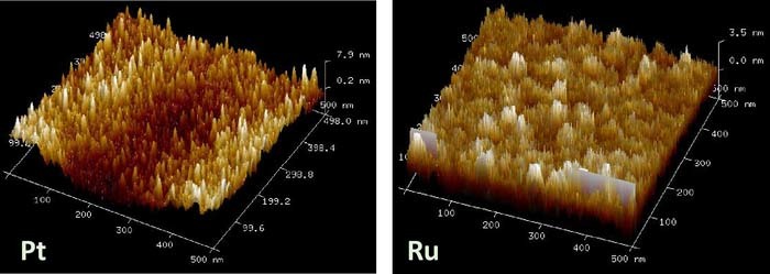
Figure 2. AFM pictures of surface roughness of Pt and Ru. The root mean square surface roughness for Pt is 2.3 nm and for Ru 1.2 nm.
Experimental Results
Electric characteristics of Cu/TaOx/Pt devices
When positive voltage applied to the Cu electrode of a Cu/TaOx/Pt is swept at a constant voltage ramp rate rr [V/s], the current will remain substantially zero until a critical voltage Vset is reached, at which a Cu conductive filament (CF) is formed connecting the Cu and Pt electrodes with each other, and the cell switches from a high resistive state (HRS) characterized by Roff (1–900 MΩ) to a low resistive state (LRS) characterized by Ron (70–15 kΩ), yielding a ratio of Roff/Ron ≈ 103−107. When the voltage is swept back, ohmic behavior is observed until a negative voltage Vreset is reached when the CF is ruptured and the current collapses to a very small value. A characteristic log-scale I-V switching characteristic of the Pt device is shown in Fig. 3. When the cell is set to an ON-state for the very first time, one speaks of forming operation, characterized by the forming voltage, Vform. The Vform is always larger than Vset, since the Cu filament has to be formed in its entirety and not partially whereas for a reset operation only a fraction of the filament has been ruptured but the entire filament not totally undone at the subsequent set operations. For Cu/TaOx/Pt devices, we find distribution Vform with a mean Vform,m = 4.6 V and a standard deviation of σ = 0.6 V, the Vset distribution with a mean, Vset,m = 2.8 V, and standard deviation, σ = 0.58 V. The rupture of the CF is triggered mainly by Joules heating at a critical current Ireset = Vreset/Ron. The Vreset distribution of our Cu/TaOx/Pt devices is characterized by Vreset,m = −0.9 V and σ = 0.32 V. These distributions apply roughly both to a multitude of devices as well as to a single device that has been switched repeatedly. In general, we observe that statistically the Vset threshold voltage tends to increase with increasing Vreset threshold voltage of the preceding reset operation. This dependence of Vset on the preceding Vreset is shown in Fig. 4.
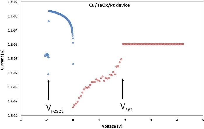
Figure 3. Set and reset operation for Cu/TaOx/Pt device (Icc = 10 μA).
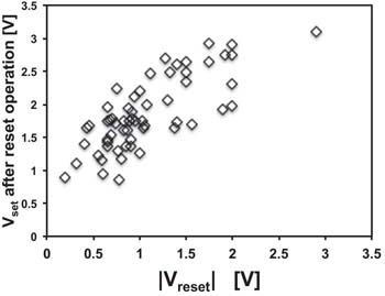
Figure 4. Dependence of Vset threshold voltage on a preceeding reset operation characterized by the reset voltage Vreset.
The endurance of the Pt devices depends on the Icc current during the set operation. For not too low Icc (>10 μA) and not too high Icc (<5mA), the device can be switched very often. Typically, in a few cases, the device was switched for 140 times and it could be still switched, but because of the lack of automatic probing station and limitation of student's physical endurance further switching cycles have been not attempted. We have also probed the retention of the devices as shown in Fig. 5. As seen in the Fig. 5 the retention of the off-state (characterized by Roff) and of the on-state (characterized by Ron) for Pt and Ru are very satisfactory. Larger off-state variations than on-state variations can be observed for the Ru devices but the noise does not compromise the retention capability as for Roff the resistance excursions are seen toward higher resistances. While the plateau of the Roff is at 200–300 M Ω, the excursions can reach GΩ range.
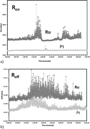
Figure 5. Retention of (a) the on-state characterized by Ron, and of (b) the off-state characterized by Roff for Pt and Ru devices.
In most instances, a compliance current Icc is imposed, lest the devices be damaged during the set operation. No Icc current limitation is applied during the reset operation. Ron of the LRS state depends on Icc via the relation 1, where the exponent n for cation filaments is very close to unity.
![Equation ([1])](https://content.cld.iop.org/journals/2162-8777/8/12/N220/revision1/d0001.gif)
The Ron–Icc relation in Eq. 1 has been reported to be valid for numerous anode/electrolyte/cathode material systems46–53 with n≈1. In Ref. 53 it has been shown that the constant A in Eq. 1 is universally correlated to the minimum SET voltage for all metallic conductive filaments reported so far. It is known54 that the compliance current enforced externally by Keithley 4200-SCS leads to a transient overshoot current especially during the very fast last phase of filament formation, as Keithley circuitry is unable to respond instantly to large current changes. In this work, where different devices are compared with one another, the effect of current overshoot should be the same for all devices, and thus the relative comparisons should still be valid.
From the Ron vs Icc plot shown in Fig. 6a, the constant A = 0.5 V and the exponent n = 1.01 are obtained by curve fitting. Here, the voltage sweep rate rr = 0.2 V/s has been used for the set operation. In Fig. 6b Vset is plotted as a function of the sweep rate. It is seen that the minimum Vset at low sweep rates corresponds to the constant A = 0.5V as predicted by the theory.53 The slope of the plot was found out to be the minimum possible value of SET voltage. Fig. 7 shows the dependence of the forming voltage and on-resistance on three different voltage sweep rates of 0.1 V/s, 0.2 V/s and 2V/s. It can be seen that not only does the forming voltage increase with increasing ramp rate, but also the on-resistance increases with increasing ramp rate. The dispersion of Ron is significantly higher at a high ramp rate compared to the one at low ramp rate. According to Eq. 1 Ron can be varied by imposing different levels of the compliance current Icc and voltage sweep rate. When the voltage sweep rate increases from 0.2 V/s to 2V/s, the constant A value of relation 1 increases from 0.5 V to 1.01 V.
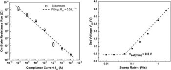
Figure 6. (a) Dependence of on-resistance Ron on compliance current Icc for Cu/TaOx/Pt device @ rr = 0.2 V/s; (b) Dependence of SET voltage on voltage sweep rate for the Cu/TaOx/Pt device (Ron @ Icc = 100 μA).
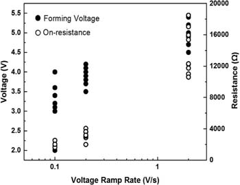
Figure 7. Dependence of forming voltage Vform and on-resistance Ron on voltage sweep rate @ Icc = 100 μA.
Fig. 8 depicts the dependence of Ron on voltage sweep rate under different levels of compliance current (5μA, 100μA and 1mA). The range of voltage ramp rate is 0.1 V/s to 2 V/s. It can be seen that Ron is larger at lower Icc, in agreement with Eq. 1. Under low compliance current (5 μA and 100 μA), Ron increases with increasing voltage sweep rate. However, in the case of high compliance current, Ron becomes independent with voltage ramp rate, indicating ohmic behavior of a robust and stable conductive filament.
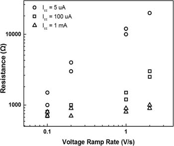
Figure 8. Dependence of on-resistance Ron on voltage sweep rate rr @ Icc = 5 μA, 100 μA and 1mA.
Typical switching cycles underlying the data in the previous diagrams are shown in Fig. 9. Here, for the sake of clearer representation, only even cycles of a 12 switching set-reset cycles are shown. The first set operation is done on a fresh cell and results in a forming voltage Vform = 3.2V. The subsequent set voltages lie between 0.7V and 2.1 V. The reset voltages are more tightly distributed and lie between −0.9V and −1.4V.

Figure 9. Even cycles of a typical first 12 switching set and reset cycles of a Cu/TaOx/Pt device.
Since filament rupturing is chiefly a thermal phenomenon, the heat conductivity of the inert electrode plays a significant role in determining the maximum temperature of the filament.
During the heating of a resistive cell A, the reset operation results in rupturing of the CF at a reset current Ires = Vres/Ron of typically a few of mA. Hence, most of the Joules heat QJH is deposited according to Eq. 2
![Equation ([2])](https://content.cld.iop.org/journals/2162-8777/8/12/N220/revision1/d0002.gif)
where Vres is the reset voltage, tres = Vres/rr is the reset time, the low reset ramp rate rr = 0.1V/s to maximize the heating during the reset.55,56 It has been shown53 that Ron depends on Icc via Ron = A/Incc given by Eq. 1, with n≈1 and A≈0.5V for Cu/TaOx/Pt devices. Depending on chosen values for Icc and rr, QJH can vary from 3 to 60 μJ. The possibility of controlling the dissipated heat in the filament in terms of compliance current, Icc, and ramp rate, rr will be important for the characterization and analysis of the electrical performance of the Pt and Ru devices.
With respect to the geometrical shape of the filament, we associate the cells with large Ron with a truncated cone with a sharp constriction of the top (see Fig. 10a), where the bulk of the Ron resistance is concentrated at the tip of the cone. Filaments with a sharp constriction at the top of the cone are easy to rupture since the maximum Joules heat is deposited at the tip (highest resistance) and leads there to a high local temperature which, in turn, leads to Cu out diffusion and formation of a gap in the filament which completes the rupture of the filament leading to the restoration of the HRS state. In contrast, the shape of Cu filament with a small Ron approaches that of a cylinder (Fig. 10b) and the temperature hot spot moves to the center (i.e. midway between the electrode interfaces) of the filament where it is much more difficult to reach high temperature (much lower resistance) and cause out-diffusion of a larger number of Cu atoms to form a gap. Experimentally, we find consistently that filament rupturing is more difficult with lower Ron resistance, i.e. formed at higher Icc (see Eq. 1).
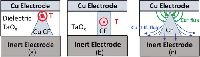
Figure 10. (a) Location of the highest temperature due to the Joules heating during reset operation. (b) cylinder-like shape of the filament with maximum temperature in midway between the electrodes. (c) Cu conductive filament with a sharp constriction at the Cu electrode interface with Cu constructive (Cu+ ion electromigration) and destructive (Cu out-diffusion) fluxes responsible for the shape of the CF.
In the set operation there are two fluxes responsible for the formation of the filament as shown in Fig. 10c at the tip of the filament there is a large voltage drop which creates high electric field between the filament tip and the Cu electrode, which allows for further transport of Cu+ ions from the Cu electrode to the filament even after establishing the initial connection between the Cu filament and the Cu electrode. The role of Icc is to limit the resulting voltage drop and thus to set a limit on the electric field driving the Cu+ ion transport. When sufficient number of Cu atoms is deposited at the tip, the resistance of the filament decreases, reducing the electric field at the tip and bringing the formation of the filament to a halt at a given Icc. When Icc is increased, then the electric field at the tip increases proportionally triggering additional arrival of Cu+ ions until the resistance of the filament drops sufficiently to reduce the electric field and thus to halt further Cu+ ion transport. The second flux is the Cu atom diffusion flux weakening the base of the filament and leads to an increased Ron resistance. The diffusion effect can be gradual in so far as any weakening of the filament leads to increased Ron resistance which, in turn, may trigger the compensating constructive Cu+ electromigration flux.
The Cu atom diffusion flux out of the filament is impacted by the thermal conductivity of the inert electrode. For the otherwise same conditions, the inert electrode with high heat conductivity will be able to remove the heat at a higher rate than an electrode with low heat conductivity. The larger heat removal rate will result in lower attainable maximum temperature. Hence, a cell with inert electrode of low heat conductivity is bound to display enhanced Cu diffusion and structural weakening of the filament. The high temperature in the filament during the reset will trigger Cu diffusion near the base of the filament partly into the dielectric, partly along the TaOx/inert electrode interface, and partly into the inert electrode if the inertness of the electrode is compromised. The net result of those diffusion components is the weakening of the base of the cone and a gradual transformation of the shape of the filament from a sharply cone-shaped into a more cylinder-shape filament as shown in Fig. 10b. Once the shape of the filament is sufficiently close to a cylinder-like shape the respective filament will be very difficult to be ruptured and the number of switching cycles comes to a halt.
Fig. 11a illustrates the SET voltage's dependence on ambient temperature and the RESET voltage's near independence on the ambient temperature. Vset and Vreset of five different cells are plotted when the ambient temperature is 20°C, subsequently increases to 85°C and reduces back to 20°C. It can be seen that the SET voltage at 85°C is reduced by ∼ 0.8V compared with the set voltages at room temperature. The reduction of Vset with increasing temperature can be explained by three different mechanisms in TaOx. (1) The ionization rate of Cu, the rate for Cu ionizes to Cu ion (Cu → Cu+ + e−), increases with increasing temperature. (2) The mobility of Cu ions in TaOx increases with increasing temperature. (3) The nucleation of Cu ions or the speed of forming the cluster of Cu at the interface of Pt electrode may also accelerate with increasing temperature, as all of those reactions are governed by Arrhenius law. We find that the RESET voltage is independent of temperature. The local temperature leading to rupturing of the filament has been reported56 to be around 900°C and therefore slight change of ambient temperature has little impact on the high local temperature responsible for the partial dissolution of the filament. The dependence of the corresponding switching currents Ireset on ambient temperature is shown in Fig. 11b as a cumulative probability distribution of Ireset at room temperature and at 85°C. It can be seen that the distribution of Ireset at room temperature is much tighter than at 85°C.
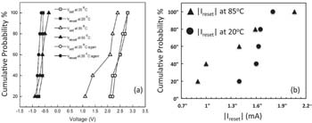
Figure 11. (a) Dependence of set voltage Vset and reset voltage Vreset on ambient temperature of 20°C and 85°C. (b) Dependence of |Ireset| on ambient temperature of 20°C and 85°C.
The metallic Cu filaments are well characterized by their temperature coefficient of resistance (TCR). For Cu filaments with Ron = 1 kΩ we find TCR(Cu) = 0.003 K−1 (which is close to the TCR of bulk Cu of 0.0039 K−1. In Figs. 12a and 12b the TCR measurement for a fragile filament (Ron = 11.2 KΩ) formed at Icc = 10 μA and for a robust filament (Ron = 250 Ω) formed at Icc = 10 mA is shown, for Pt and Ru device, respectively. For a fragile Cu filament (@Icc = 10μA) we get TCR = 0.00235K−1 (Fig. 12a) and for the robust filament TCR = 0.00362 K−1 (Fig. 12c). Very similar TCR values are found for the Ru device: for a filament formed at Icc = 10μA TCR = 0.00236K−1 (Fig. 12b) and for robust filament TCR = 0.00350 K−1 (Fig. 12c). The Cu bulk values have been verified on our Cu lines with following dimensions: thickness 150 nm, width 1 μm – 35 μm, and length 150 μm. The measurement of the TCR of the copper lines yielded consistently TCR values of 0.0388 K−1 − 0.00396 K−1, in good agreement with the TCR value of the TCR for bulk Cu of 0.0039 K−1. This is also in agreement with a study of the electric properties of freestanding Cu nanowires reported by Y. Zhao et al.58 who report that TCR for Cu nanowires decreases with decreasing of the diameter: at 230 nm TCR = 0.0038 K−1, at 100 nm TCR = 0.0033 K−1 and at 50 nm TCR = 0.0028K−1. Also A. Bid et al.59 reported TCR values between 0.004 K−1 and 0.0025 K−1 for Cu nanowires with diameters between 200 nm and 15 nm respectively. The metallic nature of the filament has also been deduced by Xiao et al.60 using ab initio atomic calculations attributed the main contribution to the conductive path along Cu-Cu metallic bonds. As seen from Fig. 12 the TCR increases with decreasing Ron resistance. Thus in both devices the electric properties of the Cu filament are the same.
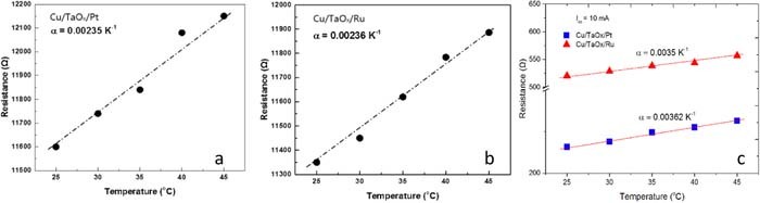
Figure 12. On-resistance, Ron, of the Cu filament of Cu/TaOx/Pt and Cu/TaOx/Ru for set operation at different Icc levels: (a) Cu CF for Pt devices @ Icc = 10 μA; (b) Cu CF for Ru devices @ Icc = 10 μA; (c) Cu CF for Pt and Ru devices @ Icc = 10 mA. The extracted temperature resistance α coefficient is indicated.
Electric characteristics of Cu/TaOx/Ru devices
The Cu/TaOx/Ru devices have been characterized in the same way as the Cu/TaOx/Pt devices. We find following distributions: for Vform a mean Vform,m = 7.3 V and a standard deviation of σ = 0.7V, for Vset distribution with a mean, Vset,m = 4.4 V, and standard deviation, σ = 0.9 V. The rupture of the CF is triggered mainly by Joules heating at a critical current Ireset = Vreset/Ron. The Vreset distribution of our Cu/TaOx/Ru devices is characterized by Vreset,m = −3.4 V and σ = 0.7 V. Thus, all the critical voltages of the Ru devices are considerably higher than of Pt devices: ΔVform = 2.7 V, ΔVset = 1.6 V and ΔVreset = 2.5 V. For Vform and Vset part of the difference can be explained by the difference of the work function between Pt and Ru of 1.65 eV, which agrees remarkably well with the observed differential for set voltages, ΔVset = 1.6V. The remaining discrepancy of about 1V can be attributed to nearly 100% higher surface roughness of Pt (2.30 nm) than Ru surface roughness (1.20 nm), as seen in Fig. 2. Higher surface roughness generates higher local fields thus allowing for filament formation at lower applied voltages. The differential in set voltage between Pt and Ru of ΔVset = 1.6V accounted solely by the work function difference, confirms this conclusion since for the set operation the surface roughness of the inert electrode is irrelevant as the gap in the filament near the Cu electrode is independent of the surface roughness of the inert electrode. In the set operation, only the gap in the ruptured filament (far away from the TaOx/inert electrode interface affected by the surface roughness) has to be closed to restore the filament. The built-in field in case of Pt electrode is the work function difference between Pt and Cu divided by the thickness of the TaOx dielectric, which in case of Pt devices comes to a quite high field of 6.8 × 10⁵V/cm. This field favors Cu+ ion transport toward the Pt electrode. The corresponding built-in field in case of Ru devices is 6 × 10⁴V/cm, i.e. one order of magnitude lower than for the Pt device. The field responsible for the formation of the Cu filament in its final stages has been estimated to be (1--2) × 106V/cm.61 The calculation of the effective fields at Vset for Pt and Ru including the built-in potential, are, indeed, in this range and approximately the same: (Δϕ(Pt,Cu)/q + Vset,m(Pt))V/25nm ≈ (Δϕ(Ru,Cu)/q + Vset,m(Ru))V/25nm ≈ 1.8 × 10⁶V/cm, in excellent agreement with.62 This analysis clearly shows that for the filament formation the local electric field is the determining factor.
The difference between Vreset voltages of 2.5V cannot be explained by the work function difference between Pt and Ru, as the main mechanism of the dissolution of the conducting filament is the Cu atom outdiffusion at high temperatures near the filament constriction. We discuss the higher reset voltage for Ru devices in more detail further below as this issue appears to be related to the issue of Ru inertness and integrity. The high built-in field for the Pt device has been verified experimentally in the following way. We have set Pt and Ru devices under three different Icc conditions of 10, 50, 100, and 250 μA and subsequently reset the devices. During the reset the ruptured gap in the filament is estimated to be ∼ 5–7 nm. This means that the built-in field in the gap would be for Pt devices 1.65V/7nm = 2.4 × 10⁶ V/cm and for Ru devices 0.1V/7nm = 1.4 × 10⁵ V/cm, i.e. more than one order of magnitude lower than for the Pt device. The built-in field for Pt device is high enough to spontaneously set the device. Indeed, experimentally we observe a spontaneous setting on a large fraction of devices after a wait time of 48 h (i.e. when the device is at 300K) after resetting the device that initially has been set at Icc = 10μA and occasionally for those set at Icc = 50μA. No spontaneous setting of the devices has been observed for Icc = 100μA. Not a single instance of spontaneous setting of the devices has been observed for the Ru devices tested at the same conditions. Thus the spontaneous forming of a ruptured filament is facilitated by the high work function difference between Pt and Cu metal electrodes. Spontaneous set operations have been also observed during consecutive switching cycles of a Pt device. After a 5th reset operation, we observed that the device was ON spontaneously, after a time of the order of tens of seconds. Here, the spontaneous formation capability of the CF has been augmented by the elevated local temperatures in the cell caused by the Joules heat dissipation leading to higher rate of Cu ionization and higher Cu+ ion electromigration mobility. This is another confirmation of the impact of work function difference between the active and inert electrode.
In Fig. 13, a typical set and reset bipolar operation for Cu CF in Cu/TaOx/Ru device is shown, corresponding to Fig. 3 for the Pt device. The Vset = 3.5 V at Icc = 10 μA and Vreset = −3 V. The bipolar switching cycles have been repeated on Cu/TaOx/Ru devices. We observe that most of Cu/TaOx/Ru devices is becoming not resettable after few set-reset operations. Thus in terms of endurance the Pt device is vastly superior to the Ru device. While the Pt devices could be switched open-ended with verified 140 switching cycles, the best Ru device had an endurance of maximally 12 switching cycles. Thus the endurance is the main weakness of Ru devices for the memory applications when compared to the Pt devices. The failure of the Ru devices after a few switching cycles is likely to be related to the geometrical shape of the Cu filament. In terms of retention, Ru devices show comparable retention as shown in Fig. 5 however, Ru retention curves are much noisier than the Pt retention curves for both the on-state and off-state. The noise of the Ru off-state curve could be attributed to the surface roughness. The noise of the Ru on-state curve is likely to be a consequence of degraded inertness of the Ru electrode. Note that during a retention test we apply a small constant voltage (of 0.05V) continuously for a long time. Although the currents are small even in the case of the on-state, the dissipated Joules heat accumulates over time and raises the temperature of the filament.

Figure 13. Set and reset I-V characteristics for Cu/TaOx/Ru device with Icc = 10 μA imposed during the set operation.
As in the case of Pt devices, Ron for Ru devices also depends on the compliance current, Icc. On a double logarithmic scale, on can see that Ron also decreases linearly with increasing Icc conforming to the Eq. 1. As is shown in Fig. 14, the extracted parameters are A = 0.61 V and n = 1.08. The condition for the set operation is: voltage sweep rate rr = 0.2 V/s. It can be concluded that Cu/TaOx/Ru devices has slightly higher constant A value than Cu/TaOx/Pt device when the set operation is the same (rr = 0.2 V/s). As shown elsewhere53 with the exponent of Icc in the denominator of Eq. 3 being close to 1, the constants 0.5 V and 0.61 V can be interpreted as the lowest possible Vset voltages under which the Pt device and Ru device, respectively, can be set at a given voltage ramp rate. Lowest value for the constant A can be reached as a limiting case for very slow voltage ramp rates. The difference in the minimum set voltage extracted from Ron - Icc characteristics confirms that the Vset voltage for Ru devices is higher than for Cu device.

Figure 14. Dependence of on-resistance, Ron, on compliance current, Icc, for the Cu/TaOx/Ru device @ rr = 0.2 V/s.
Since in Pt and Ru devices the filament is made of Cu atoms one would expect similar temperature coefficients of resistance. In Figs. 12b and 12c, we found TCR (Ru) = 0.00236 K−1 and TCR(Pt) = 0.00235 K−1 for similar values of Ron which, within the accuracy of our measurement, means that the values are identical. Therefore, we conclude that under a positive voltage stress applied to the Cu electrode, Cu conductive filaments are formed in both devices. Moreover, these values are consistent with TCR values of Cu CFs observed in many other devices. It has been observed that for both devices TCR increases with decreasing Ron reaching a value of 0.0035 K−1 at Ron = 300 Ω as seen in Fig. 12c.
To summarize the characterization of Ru devices one can state that with the proviso that all critical threshold voltages, Vform, Vset, and Vreset are higher than for Pt devices which can be partly understood in terms of work function and in terms of differences in surface roughness difference between Pt and Ru, Pt and Ru devices behave very similarly. There are, however, two major differences: (i) Vreset is much higher in Ru than in Pt devices, and (ii) and the endurance in terms of the maximum number of sequential set-reset cycles for Ru (at most 12) is substantially lower (maximum than for Pt devices (more than 140), particularly when the devices are set at Icc>100μA, i.e. for low Ron values. We address those two issues in the subsequent sections in more detail.
Degraded endurance of Cu/TaOx/Ru devices
The major drawback of the Ru device is that while Pt devices can be switched repeatedly back and forth for at least 140 times, Ru devices are becoming non-resettable after several set-reset operations (less than 13) and sometimes after the first set operation when the set operation is performed at high Icc. In some cases, it was even difficult to reset a high resistance Cu filament in a Ru device formed at Icc as low as 5 μA. The failure of the Ru devices to switch after several switching cycles is likely to be related to the geometrical shape of the Cu filament.
It is known that even in Pt devices, it is difficult and sometimes impossible to reset the cell if the cell has been set at high Icc. This phenomenon may be explained by different geometrical shape of the conductive filament. For low Icc the shape of the CF can be approximated by a truncated cone as shown in Fig. 10a where the bulk of the CF's resistance resides in the tip of the cone. Since during the reset the power dissipated in the filament is equal to Ireset2 × Ron, the highest temperature is reached in the constriction at the tip of the cone, where the rupturing of the filament is easy, as shown in Fig. 10a. At high Icc (as seen in Fig. 13 Ron vs Icc) the Ron decreases sharply by adding Cu atoms to the upper section of the cone. Therefore, the shape of the filament becomes more and more cylindrical as shown in Fig. 10b. In this case, the maximum temperature, in absence of any pronounced constriction, is reached in the middle section of the cylinder, where the low resistance filament is relatively strong. Hence, rupturing of the CF becomes difficult or impossible.
The cylindrical shape of the CF may be also obtained if the base of the cone in contact with Ru electrode is eroded, see Fig. 15a. As the bottom base of the CF is reduced while new Cu+ ions are added from the top during the set operation, the shape of the filament will tend to assume a cylindrical shape. There are several possible mechanisms for the erosion of the base of the cone: (i) Cu surface diffusion along the Ru interface to which has been alluded before in the context of the much larger Vform for Ru than for Pt devices, (ii) crystallization of Ru and out-diffusion of Cu along the Ru grain boundaries, (iii) Cu and Ru chemical reaction with oxygen and/or with Si. Those mechanisms are depicted in Fig. 17 and will be discussed further below.
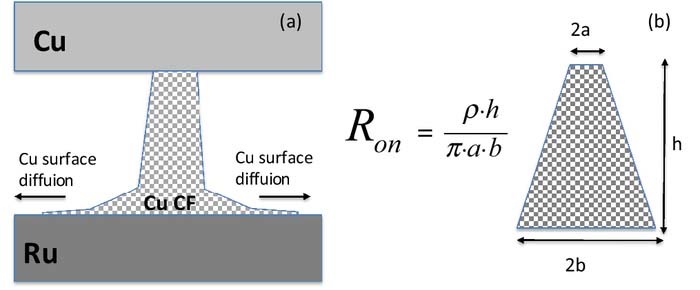
Figure 15. (a) Hypothesized geometrical shape of Cu conductive filament structures for Cu/TaOx/Ru device with a degraded base at the TaOx/Ru interface, (b) Truncated cone shape of a conductive filament with the equation (Eq. 3) for on-state resistance, Ron, for a truncated cone geometry.

Figure 17. Switching operation of Ru device B with the modified substrate with TaOx inserted between Ti and SiO2 @ Icc = 1μA, rr = 2V/s: a) forming operation with Vform = 3.95V b) reset operation with Vreset = −2.1V, c) set operation with Vset = 3.8V.
To keep the Ron constant, the loss of Cu atoms at the base of the cone has to be compensated by additional flux of Cu+ ions explaining the need for higher forming voltages in Ru devices in excess of the work function difference of 1.6V. Whereas, with a nearly perfect stopping power, the shape of the filament in the Pt device can be assumed to be conical with more or less sharp tip at the Cu electrode, the shape of the Cu filament in the Ru device is more cylinder-like especially if the Ru device is undergoing several set-reset switching cycles. These mechanisms appear to be very similar to the properties of Cu/TaOx/Ta devices observed in Ref. 44.
The on-resistance of a conically shaped resistor is given by:
![Equation ([3])](https://content.cld.iop.org/journals/2162-8777/8/12/N220/revision1/d0003.gif)
where h is height, a is the radius of the truncated cone base at the top, b the radius of the base at the bottom, and ρ is the specific resistivity of the filament, see also Fig. 14b. To demonstrate the difference between the hypothesized shapes for the Cu CF for the Pt and Ru device, we have constructed two cone shapes with the same overall CF resistance, Ron: we assume following parameters for the Pt device bPt = 3 nm and aPt = 0.5nm and for Ru device bRu = 1.76 nm and aRu = 0.85 nm, for a common height h = 25 nm. Based on Eq. 3, the resistances of Cu CFs for Pt and Ru devices are 15,923 Ω and 15,966 Ω respectively, which are almost the same values shown in Fig. 6a and Fig. 13 when the devices are set at Icc = 10 μA. However, the geometrical shape is very different. Here, the resistivity of copper filament has been assumed to be ρ = 300 × 10−6 Ω·cm.62 This demonstrates that the two filaments of the same Ron resistance (enforced by the same Icc current) may have substantially different geometric shape. The different shape of the filament has an impact on the reset operation and the endurance properties of the device.
Impact of embedment on the performance of Cu/TaOx/Ru devices
To study the relative degradation of Cu/TaOx/Ru vs Cu/TaOx/Pt devices, we have manufactured two nominally identical Cu/TaOx/Ru devices (where the layers of the cell proper have been manufactured at the same time) however embedded differently on the Si wafer. While the substrate for Ru device A is the same as for the Pt device, i.e. Ti(20nm)/SiO2(730nm)/Si-wafer, the Ru device B is manufactured on the layer stack Ti(20nm)/TaOx(30nm)/SiO2(730nm)/Si-wafer. Thus, Ru device B has an additional TaOx-30nm layer inserted between SiO2 and Ti layers. The electrical characterization of the two Ru devices, A and B, has been guided by the hypothesis that the difference in electric performance between the two devices is caused by effects stemming from larger or smaller exposure to the Joules heating dissipated in the device. Therefore, the form/set operations have been performed at low and high Icc currents, i.e. Icc = 1 μA, 5 μA, 10 μA, and 50 μA. Clearly, once the filament is formed exposure to Joules heating effects at Icc = 50 μA should be larger than at Icc = 1 μA, see Eq. 2. To control the heating effects even further, also during the reset operation, we have varied the reset voltage ramp rate, rr, between 0.2V/s and 2V/s, see Eq. 2. In the reset operation the currents flowing through the cell are large; on the order of a few mA. Therefore, low ramp rate implies larger heating because of longer duration of exposure to high currents flowing through the filament, before the cell is ruptured at a reset current, Ireset. Thus, most heating would occur for Icc = 50 μA and rr = 0.2V and least heating for Icc = 1 μA and rr = 2.0 V/s, see Eq. 2.
In general, we find that the Ru device B with the additional TaOx layer inserted between SiO2 and Ti shows much better performance than the Ru device A (i.e. without that TaOx layer) at all test conditions. However, the degree of the improvement in the switching properties of Ru cell B over cell A varies with the levels of applied compliance current and ramp rate. The highest improvement is found for Icc = 50 μA and rr = 0.2V/s (high heat dissipation), and almost no difference in performance between the two devices can be observed for the condition Icc = 1 μA and rr = 2.0V/s (small heat deposition). A typical successful forming, reset, and set I-V characteristics for device B are shown in Fig. 17. No I-V characteristics of comparable quality can be shown for the device A; its best behavior is shown in Fig. 16.

Figure 16. Switching operation of Ru device A with the same substrate as the benchmark Pt device @ Icc = 1μA, rr = 2V/s: a) forming operation with Vform = 4.9V b) reset operation with Vreset = −2.5V, c) set operation with Vset = 3.1V.
There exists a significant difference in endurance between the two Ru devices differently embedded on the substrate. We find that at Icc = 50 μA and rr = 0.2V/s the Ru device A does not display resistive switching behavior at all, i.e. its endurance is nil. The device A cannot be reset after the filament has been formed the very first time. However, when the reset ramp rate is increased fivefold to rr = 1V/s – thus reducing the Joules heat dissipated in the device - the device A can be neither set or, if the set operation is eventually successful, the device cannot be reset, i.e. the resistive switching cell has been permanently damaged. During the set operation, even if successful, no sharp set transition can be observed but rather a gradual transition to the conductive state characteristic for a dielectric breakdown. In contrast, device B with the additional TaOx layer at the bottom shows some resistive switching behavior for a few cycles (maximum 6). Sharp formation and set characteristics are observed with Vset between 2.6 V and 4.0 V, however the subsequent reset attempts have proved unsuccessful. The frequency of devices B displaying resistive switching behavior is quite low at about 1% of the devices B tested. We conclude that high heating effects are detrimental to both devices. But, while device B displays some (if small) degree of resisting switching behavior (5-6 switching cycles), device A does not display resistive switching at all.
Keeping the reset ramp rate at 0.2V/s but now reducing the Icc current from 50 μA to 1 μA, we observe improved resistive switching behavior for both devices with the frequency of the Ru devices B being twice as high (maximum 22 cycles) as for the Ru devices A (maximum 10 cycles). Thus, at low heat dissipated in the cell, the endurance of the Ru device B is 22 switching cycles while the Ru device A exhibits 10 switching cycles.
The switching behavior improves even more when we keep Icc at 50 μA and increase the ramp rate from 0.2V/s to 2.0V/s for both devices. Now both devices show some resistive switching behavior, however, again, the frequency of resistive switching is at least three times higher for the device B (maximum 30 cycles) than for device A (maximum 11 cycles). Thus again the Ru device B shows a superior endurance over the Ru device A. Clearly, reduced thermal budget due to the faster voltage ramp rate improves resistive switching behavior of both devices. Table I shows comparison of the Vform, Vset and Vreset for both devices.
Table I. Comparison of threshold voltages and Ron for Ru devices A and B, both set at Icc = 50 μA and rr = 2.0 V/s.
| Device | Vform [V] | Vreset [V] | Vset [V] | Ron [kΩ] |
|---|---|---|---|---|
| A (Ti/SiO2) | 4.6 – 5.0 | 1.7 – 3.6 | 2.8 – 4.5 | 13 – 42.0 |
| B (Ti/TaOx/SiO2) | 2.9 - 4.5 | 1.5 – 3.3 | 2.5 – 3.6 | 10 – 20.0 |
It can be seen that Vform for device A is higher 4.6 V < Vform(A) < 5.0 V than Vform, for device B 2.9 V < Vform(B) < 4.5V. A similar observation applies to Vset. This behavior could be explained by the assumption that Cu loss of the filament for device A is higher than for device B. It can also be seen that the reset and Ron values for devices A and B are comparable. This indicates that once a Cu filament is established the dynamics of the creation of a gap in the filament during the reset operation are the same.
Table II shows the values for the same quantities as in Table I but now for Icc = 1 μA and rr = 2.0V/s. Comparing Table I and Table II we find the same trends described above in Table I. The frequency of the devices B tested that display resistive switching behavior is now very high at 100%, while the frequency for the devices A tested showing resistive switching behavior is about 2% for the same switching conditions. Manifestly, the least amount of heating produces best resistive switching behavior for device B.
Table II. Comparison of threshold voltages and Ron for Ru devices A and B, both set at Icc = 1 μA and rr = 2.0 V/s.
| Device | Vform [V] | Vreset [V] | Vset [V] | Ron [kΩ] |
|---|---|---|---|---|
| A (Ti/SiO2) | 4.9 | 2.6 | 1.6 – 3.4 | 3.0 – 4.0 |
| B (Ti/TaOx/SiO2) | 3.8 – 4.2 | 1.5 – 3.5 | 2.8 – 3.0 | 2.0 – 16.0 |
We have measured device A and B set also at very high Icc = 0.5 mA at which a robust filament with a low resistance Ron is being formed. We find the same trends as found at lower Icc current levels. Interestingly, for rr = 2.0V/s the frequency of resistive switching is about the same at 60% for both devices. However, when we lower rr from 2.0V/s to 0.2V/s, i.e. allow for more Joules heating, the frequency of device A drops to 17% while the frequency of devices B stays constant at 60%. Thus again, Ru device B is much less sensitive to dissipated Joules heating than the Ru device A. This clearly demonstrates that the endurance of the device is directly related to the amount of heat deposited in the device.
Finally, we have compared two I-V characteristics of both devices at the same stress conditions with very low Icc: Icc = 1 μA and rr = 2V/s. The first measurement was taken on a fresh device. The second measurement was taken on a fresh device that has experienced resistive switching at Icc = 50 μA and rr = 2V/s, prior to the measurement at Icc = 1 μA. Thus in the second case the device has experienced considerable "pre-heating" at Icc = 50 μA. We find that both devices A and B perform worse after they have been "preheated" at Icc = 50 μA. While in the case of device B some of the devices exhibit resistive switching, there was almost no resistive switching for the device A. This means that at the operation at Icc = 50 μA, some irreversible changes must have taken place within the memory cell. On the other hand, the same experiment with "pre-heating" at 1 μA did not affect the subsequent resistive switching of both devices demonstrating again that heat dissipated in the cell is the key factor in designing optimum endurance of the cell.
Degraded Inertness of the Ru Electrode
Causes for high sensitivity of the Ru device to Joules heating
There is a sizeable circumstantial indirect evidence from the extant literature pointing to a possible cause of the degraded behavior of Ru device A vs Ru device B. During the forming and set operations a substantial local heating of the filament takes place. The maximum temperature has been estimated to be between 600°C and 1000°C.57,63--65 Regner and Malen66 have argued that because of the nm dimensions of the filament the thermal transport is non-diffusive and the differential Fourier equation of heat transport is grossly inadequate. The solution of the more adequate Boltzmann transport equation leads to much higher temperature estimates,66 as high as 1000°C. Our hypothesis is that such high temperatures even at relatively short times of microseconds up to seconds can activate Si diffusion from the SiO2 layer through the thin Ti layer into Ru layer, possibly accompanied by a TiOx reaction. The Ru layer, in turn, can undergo, at such high temperature, local crystallization creating grain boundaries along which Si may readily diffuse.67 Thus Si that may reach at the Ru/Ti interface, may induce Ru silicide reaction to RuxSiy and/or it can travel along the Ru grain boundaries and trigger Cu silicide reaction CusSit at the forming base of the Cu filament at the Ru/TaOx interface.68 Both silicides are known to be poor diffusion barriers for Cu atoms.68 The possible degradation mechanisms of the Ru electrode are shown conceptually in Fig. 18. Those degradation mechanisms may also explain the low frequency of resistive switching behavior for the Ru device A when compared with the Ru device B. For both devices, the worse performance is found when the base of the Cu filament overlaps with a possible Ru grain boundary. In this case, the Cu atoms may be drained out of the filament through Cu diffusion along the grain boundary. The best case scenario for resistive switching is when the Cu filament does not overlap significantly or at all with a grain boundary. In that case the resistive switching behavior in both devices could be comparable. The non-overlap case may be responsible for the few instances when good resistive switching behavior can be observed for device A. In case of device A, the silicide reactions may lead to inclusions of RuxSiy and CusSit most likely along the grain boundaries and, hence, such inclusions widen the area at the Ru surface where Cu can easily diffuse into the electrode. Therefore, Ru device A should suffer from Cu in-diffusion more than device B. Both Ru and Cu silicide reactions, compromise the inertness properties of the Ru electrode and entail depletion of Cu atoms from CF into Ru electrode. The motivation of inserting TaOx layer between Ti and SiO2 layer in device B, has been to stop - or at least reduce - the Si diffusion into the Ru electrode. Our experimental results presented and discussed below seem to confirm it showing that in case of device B the degradation of the Ru electrode due to silicide reactions and Ru crystallization has been reduced, even if still short of a complete suppression. The TaOx layer of only 30 nm deposited by PVD is known to form tantalum oxide with lower density and higher porosity than the stoichiometric Ta2O5 deposited by Atomic Layer Deposition (ALD). Thus the inserted 30 nm TaOx layer may still not be a perfect diffusion barrier for Si, either. Third integrity issue is the adhesion of Cu atoms to Ru interface. It is known that Cu has a low wetting angle on Ru (43°)68 and high affinity to Ru surface.69 Therefore, Cu adheres strongly to Ru surface even at high temperatures as high as 600°C.70,71 These findings argue strongly against significant Cu surface diffusion on Ru surface. This argument is further corroborated by the significantly higher surface roughness of Ru than that of Pt. Higher surface roughness is less conducive to surface diffusion. However, at 475°C and above Cu starts to diffuse through the energetically favorable inter-grain boundaries of Ru columnar microstructure.67

Figure 18. Possible mechanisms of the hypothesized degradation of the Ru electrode. Elevated local temperatures in the immediate vicinity of the filament may cause Si diffusion into Ru, possibly along Ru grain boundaries and lead to RuxSiy reactions. Cu may use the Ru grain boundaries as diffusion paths and undergo a silicidation reaction.
These three reliability issues may conspire to cause substantial degradation of the inertness properties of the Ru electrode and trigger enhanced Cu diffusion through the degraded Ru electrode. The existing Ru2Si3 may accelerate the Cu diffusion even further.67,72 At 550°C, Cu can completely diffuse through a 20 nm Ru film, penetrate into the Si substrate, and form Cu3Si by interacting with the substrate and eventually completely nullifies the barrier inertness properties of the remaining Ru layer.67,69 The Cu3Si is found to be morphologically inverted pyramid-shaped rectangular crystallites with orientation perpendicular to the substrate.73,74 Such isolated crystals form a rough surface and induce a permanent damage to the Cu metallization in CMOS BEOL. Similar damage is most likely being done to the Cu filaments in our devices. Although, ideally both Ru and Cu are relatively inert on thermally stable SiO2 even at high temperatures, the direct reaction with Si causes barrier failure at the same temperature for both Si and SiO2 substrate.75 Thus, the temperature at which Ru2Si3 forms may be the key triggering factor for the degradation of the inertness properties of Ru.72
Given the degradation mechanisms described above, some mitigation strategies may be considered. One is a deposition of a thicker Ru electrode (presently at 50 nm). However, because of the columnar grain structure thicker Ru layer is not likely to be of much help. The other approach would be to limit the temperature of filament rupturing. This is difficult to achieve since the rupturing temperature appears to be an intrinsic property of the device. The formation of Ru2Si3 requires higher temperature than formation of Cu3Si,72 but it can be reached readily during a filament formation or filament rupture. Indeed, it has been shown that the barrier functionality of Ru film fails completely at ∼700°C irrespective of the Ru layer thickness.72
In conclusion, applying above observations to the circumstances encountered in our devices, it is plausible to argue that the insertion of the TaOx layer between SiO2 and Ti leads to a suppression of Si diffusion which leads, in turn, to a suppression of Ru and Cu silicide reactions. Since Ti is known to be an aggressive oxygen getter, the TiOx at the interface of SiO2 frees up Si atoms that can then readily diffuse into the Ru layer. The insertion of TaOx layer between Ti and SiO2 appears to act as an effective Si diffusion barrier.
To find a tangible evidence for the compromised inertness of the Ru we have considered direct physical analysis techniques SIMS and XRD. However, Secondary Ion Mass Spectroscopy (SIMS) is inadequate to measure copper or oxygen content in Ru electrode. The number of Cu atoms in a filament at the base of the cone interfacing the inert electrode can be estimated to be 50 atoms with a base of 50 nm2. If of these atoms 1/10 or less would diffuse into Ru, most likely along the grain boundaries, it would result in a concentration of Cu atoms in Ru of at most 1012 cm−3 in a tiny volume of less than 1000 nm3 with a density of the matrix material of typically 1022 cm−3, while other neighboring volumes with still much lower concentration. Such tiny average concentrations of copper or oxygen are well below the sensitivity of SIMS which is typically at most 1014 cm−3. Moreover, the matrix material, here the Ru electrode, is only 50 nm thick and typically 10 μm wide. SIMS cannot work on such thin and narrow layers because the sputtering yield would be far insufficient. Usually the SIMS crater when using Cs or O ions as the bombarding species is several hundred microns wide.
A more promising physical analysis technique is X Ray Diffraction (XRD) which is presented next.
XRD studies of layer systems for Ru devices A and B
We have performed extensive XRD studies on the substrates for Ru devices A and B, see Fig. 1 i.e. Cu(25nm)/Ru(50nm)/Ti(40nm)/SiO2(611nm)/Si for device A (the same substrate as for the Pt device) and, Cu(25nm)/Ru(50nm)/Ti(40nm)/TaOx(27nm)/SiO2(611nm)/Si for Ru device B. In order to extract the significant XRD signals, we have manufactured following auxiliary samples 1) Si (Si wafer with native oxide), 2) SiO2(611nm)/Si, 3) Ti(20nm)/Si, 4) TaOx(27nm)/Si, 5) Ru(50nm)/Si, 6) Cu(25nm)/Si, 7)Cu(25nm)/SiO2(611nm)/Si, 8) Ru(50nm)/SiO2(611nm)/Si, 9) TaOx(27nm)/SiO2(611nm)/Si, 10) Ti(40nm)/SiO2(611nm)/Si 11) Ti(20nm)/TaOx(27nm) /SiO2(611nm)/Si, and 12) Ru(50nm)/Ti(40nm)/SiO2(611nm)/Si. The auxiliary samples serve the purpose to track the XRD peaks with added layers to the existing stack, and help identify background signals in order to extract the relevant signals pertinent to Ru devices. The XRD measurements have been performed on the aforementioned samples for three annealing conditions: i) unannealed, i.e. at 300K, ii) annealed at 600°C for 10 min, and iii) annealed at 900°C for 30 min. While an extensive study of this XRD study will be published elsewhere,76 the results relevant to Ru devices A and B are summarized below. We observe a Ru crystallization peak at 42.15° of the XRD spectra on all samples that display a Ru layer after the samples at room temperature and after an anneal at 600°C, and 900°C. This is in agreement with XRD studies of similar layer systems reported in Ref. 77. XRD signals for samples of Ru/Si at 300K, Ru/Si after an RTP anneal at 600° C for 10 min, and for Ru/SiO2/Si after an anneal at 600°C for 10 are shown in Fig. 19. It is seen that a Ru3Si2 crystallization peak appears at 600°C. We observe also on some samples an XRD peak (or shoulder observed next to a broad Si wafer peak) of ruthenium silicide Ru2Si3 at 44.7° only after 900°C anneal as shown in Fig. 19. This is in agreement with observations of Ru3Si2 XRD detection made in Ref. 68. We observe this peak on the following samples: Ru/Si, Ru/SiO2/Si, Ru/Ti/SiO2/Si, and Cu/Ru/Ti/SiO2/Si. The strongest Ru3Si2 signal can be seen for the Ru/Si and Ru/SiO2 samples. From comparison with Fig. 19 it can be seen that the XRD signal at 44.7° is absent after an anneal at 600°C and also for unannealed sample Ru/SiO2/Si. However, for samples Ru/Ti/TaOx/SiO2/Si and Cu/Ru/Ti/TaOx/SiO2/Si the Ru3Si2 shoulder is either not there or very weak, as shown in Fig. 20. From Fig. 19 it is also seen that the Ru3Si2 peak at 41.7° disappears at 900°C, again in agreement with observations made in Ref. 77. We conclude that TaOx layer inserted between SiO2 and Ti acts as a Si diffusion barrier, and hence suppresses the Ru silicidation reaction.

Figure 19. XRD spectra of three layer structures: Ru/SiO2/Si as deposited, Ru/Si and Ru/SiO2/Si after a 600°C 10 min anneal. The Ru crystallization peak has been also observed at other layer structures with a Ru layer only after a 600°C anneal. The peak is very weak at room temperature and disappears after an anneal at 900°C for 30 min.
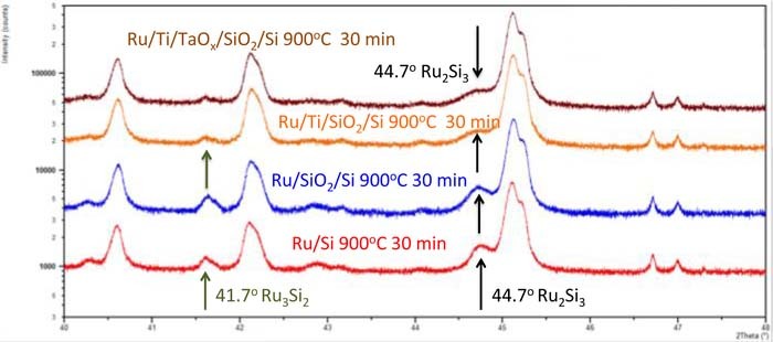
Figure 20. XRD spectra of four layer structures annealed at 900°C for 30 min: Ru/Si, Ru/SiO2/Si, Ru/Ti/SiO2/Si and Ru/Ti/TaOx/SiO2/Si. On all structures a Ru2Si3 shoulder can be observed at 44.7°C next to a large signal 45.12°C which stems from the Si wafer as verified by XRD spectra on Si and SiO2/Si structures.
We do not observe any XRD peaks related to copper silicide reaction. The lack of a clear Cu3Si signal may not necessarily eliminate this reaction altogether, but points, at least, to scarcity of the compound which could be formed along the Ru grain boundaries which is a confirmation of our assessment of Cu detectability by SIMS discussed before.
As Ru is easy oxidizable even in ambient atmosphere we were looking for a RuOx XRD signal. It is well known that RuO2 has characteristics XRD peaks at 2θ = 30°, 35°.78,79 No RuOx signal could be detected even on free Ru surface samples annealed at 600°C and 900°C in our samples. No direct oxidation of Ru at an elevated temperature in a furnace has been performed as RuOx was not planned for part of the manufactured layer system shown in Fig. 1b and Fig. 1c. The lack of an XRD signal does not per se preclude existence of a native oxide. But it indicates that either the RuOx is amorphous or that there is an insufficient quantity of crystalline RuOx to produce an XRD signal.
The XRD study confirms that the inertness of the Ru electrode is impaired by Ru crystallization at temperatures around 600°C and due to Ru silicidation at 900°C. The XRD study corroborates not only the difference in electrical performance between Pt and Ru device but also among the Ru devices embedded on different substrates.
Summary
Cu/TaOx/Ru devices compared to Cu/TaOx/Pt devices have higher forming, set, and reset voltages which can be partly attributed to the work function difference between Pt and Ru of 1.6 eV and partly to the significant difference in surface roughness between Pt and Ru. The performance deterioration of Ru devices is particularly conspicuous when the cell is exposed to high Joules heat dissipation during the set and reset switching cycles. At low Joules heat dissipation the switching performance of both Ru and Pt devices is comparable. The Joules heat dissipation in a major factor determining the endurance properties of the device. While the maximum number of switching cycles of the Pt devices is, in many cases, unlimited (more than 140), in case of Ru, is limited to 12 under most favorable circumstances. In the extreme case of high Joules heat, the number of switching cycles for Ru device is limited to only one cycle. Thus, Joules heat dissipation is the major limiting factor for the endurance of all devices characterized in this work. The integrity of the inert electrode appears to have a major impact on the Cu diffusional fluxes which in turn, determine the geometrical shape of the Cu conductive filament. The Pt electrode with its excellent stopping power produces conical filament with a sharp constriction near the Cu electrode interface, whereas in case of Ru electrode, the loss of Cu ions at the base of the Cu filament leads to a more cylindrical shape of the filament which prove more difficult to rupture in a reset operation. However, Pt with its highest work functions among the metals, induces high built-in electric field in the device which may reach critical fields in the ruptured filament's gap leading to spontaneous set operation, as demonstrated experimentally.
It has also been demonstrated that the electrical switching properties of the nominally the same resistive switching device Cu/TaOx/Ru, however embedded differently on the wafer (Cu/TaOx/Ru/Ti/SiO2/Si vs. Cu/TaOx/Ru/Ti/TaOx/SiO2/Si), differ substantially. This is the result of chemical and structural interactions of the device proper with its immediate environment which is brought about by the nanometer dimension of the layers involved and significant heat deposition during the switching of the resistive switching cell. This finding points to the broader and critical impact of the device's embedment on its structural, material integrity, and, eventually, its electrical reliability and endurance properties. In the particular case of this investigation, we attributed the significant degradation of the integrity of Ru electrode to Ru grain crystallization and to ruthenium silicidation, which have been confirmed by extensive XRD studies. The insertion of a TaOx layer between the SiO2 and Ti layer has led to a suppression of the Ru crystallization and silicidation reaction and thus to an improved electrical performance and endurance of the Ru device on the Ti/TaOx/SiO2/Si substrate as compared to the Ru device manufactured on the Ti/SiO2/Si substrate.
ORCID
S. W. King 0000-0001-5400-7679
Marius Orlowski 0000-0002-1425-4058