Abstract
Gate and drain current transients following the application of a step/pulse reverse bias to the gate of AlGaN/GaN HEMTs can be described by a superposition of 2–3 extended exponents with characteristic times of the main process having activation energy of 0.7–0.8 eV. The drain current relaxation is a consequence of charge trapping and movement in the AlGaN barrier. A qualitative model explains this process by movement of a step of charge trapped on deep states in the barrier and movement of the step toward the interface by multiple emission/capture hops. The process is assumed to be confined to channels in AlGaN (presumably dislocations) surrounded by potential barriers, preventing effective injection of the carriers into the channels with forward bias pulses. The model qualitatively explains the often reported appearance of hole-trap-like signals in deep level studies of AlGaN/GaN HEMT structures and the persistent changes in capacitance and current of these structures occurring upon pulsing and illumination.
Export citation and abstract BibTeX RIS

This is an open access article distributed under the terms of the Creative Commons Attribution 4.0 License (CC BY, http://creativecommons.org/licenses/by/4.0/), which permits unrestricted reuse of the work in any medium, provided the original work is properly cited.
One of the most serious problems with III-Nitrides- based high electron mobility transistors (HEMTs) is the phase delay of the drain current upon pulsed change of the gate bias, so called "gate-lag".1–3 This phenomenon causes increase of the switching time and long-term drift of the threshold voltage and the drain current. The generally accepted view is the gate-lag is caused by trapping of electrons flowing from the gate at high reverse voltage and subsequent capture of electrons by deep centers under the gate. Both the capture and emission process from these traps can be studied by analysis of gate and drain transients as a function of pulsing conditions and temperature by using current or capacitance deep level transient spectroscopy (CDLTS or DLTS)2–5 or by direct measurements of individual transients.1,6–9
These measurements provide the concentration and position of the traps involved and their capture cross sections. This is complicated by the presence of multiple traps, strong non-uniform electrical and strain fields, and the contribution of the band-like states related to extended defects and to surface or interface states. As a result, the drain and gate current relaxation curves are non-exponential. A common approach is the deconvolution of the actual relaxations into a sum of independent exponential relaxations and fitting the pre-exponential coefficients to experiment.6 Various methods to improve the convergence and reproducibility of the procedure exist.7,8 Another popular approach is to build the derivative of the relaxation curve on the logarithm of time, find the peaks in such plots, and trace the peak position variation with temperature to extract the activation energy and capture cross section of the traps.2,3,9 The number of peaks in either approach is quite limited (typically, 2–3) in either method,9 but the peaks are generally broad which requires invoking a large number of exponents to attain good fit in the basic method,6 while providing no knowledge on the physical nature of broadening. Good fits can be achieved when using 2–3 extended exponents describing capture and emission in the presence of broadened barriers for capture, or by Gaussian broadening of the logarithm of relaxation time describing broadening of the discrete level into Gaussian energy bands.9 The advantage of this approach is the much faster convergence while providing physically meaningful parameters of the broadening process.
One of the things that still requires better understanding is the frequent observation of the capture process being thermally activated, with the activation energy of 0.4–0.9 eV.6,9–11 In the basic model this activation energy comes from the activation energy of reverse current in HEMT.1,6 However, in actual measurements the temperature dependence of reverse current is small which is often explained by the current flow being determined by combinations of Poole-Frenkel and Fowler-Nordheim mechanisms.12–14 In many cases, the current and capacitance relaxations in AlGaN/GaN HEMTs show not only electron-trap-like transitions natural for a majority carrier device such as a HEMT, but also hole-trap-like signals.9,15–17 In this paper, we suggest both phenomena (i.e. temperature activated capture with no temperature activated current and the appearance of hole traps signals) can be attributed to multistage process involving deep traps in the AlGaN barrier emitting and subsequently capturing electrons, forming a step in the space charge moving toward the AlGaN/GaN interface.
Experimental Methods and Data Treatment
The HEMT structures were grown by metallorganic chemical vapor deposition on Si (111) or semi-insulating 4H-SiC substrates. The structure henceforth called HEMT1 has been described in detail previously.10 In brief, the 0.8-μm-thick unintentionally doped GaN buffer with 50-nm-thick channel layer and 20 nm undoped AlGaN (25% Al) barrier were grown on the substrate using AlGaN strain-relieving layer. The source-drain spacing was 5 μm, the gate was of the multi-finger type with the length of 0.5 μm and total width of 8 mm. The device passivation was done by SiNx, the device isolation was achieved by N+ multiple energy ion implantation. The other structure, called below HEMT2, was grown on semi-insulating 4H-SiC. It consisted of AlN nucleation layer, followed by the graded AlGaN strain-relieving layer, then by 4 μm semi-insulating GaN(Fe) buffer of which the top 100 nm was left undoped (this portion of the buffer was lightly n-type conducting). On top of this buffer, an AlGaN barrier with thickness 20 nm and Al composition of 27% was grown. The source -drain separation was 5 μm, the multifinger gate length was 0.5 μm with the total gate width of 12 mm. The device isolation and passivation were done in the same manner as for HEMT1.11
Current-voltage (I-V) measurements and drain and gate current transients following the pulse or step of gate voltage were measured in the temperature range 280–470 K for time periods up to several thousand seconds with time steps of 10−4 s or longer using a hot stage. Detailed results of static and pulse I-V characteristics of both types of structures have been described elsewhere.10,11 The threshold voltage for the HEMT1 structure was ∼ −2 V. For the HEMT2 structure it was ∼ −4 V.10,11 The amount of current collapse due to gate-lag was considerably higher for the HEMT2 than for the HEMT1 structures. Consequently, the former also showed a more pronounced hysteresis in I-V characteristics and a stronger shift of the low-temperature capacitance-voltage (C-V) characteristics dependent on the gate voltage at which the structure was cooled.10,11
Fitting of the waveforms of the drain current and gate current relaxations and their derivatives by the logarithm of time were carried out.9 In brief, the current relaxation curve was represented as a sum of several (usually, 1–3) decay curves of the extended exponent form:
![Equation ([1])](https://content.cld.iop.org/journals/2162-8777/6/11/S3034/revision1/d0001.gif)
where the broadening coefficient β describing the change in the relaxation time, τ, as the decay progresses with time t, is in the range 0 < β ≤ 1 (Io in Eq. 1 is the constant current whose magnitude does not change with time, A2 is a constant). Differentiating Eq. 1 by the logarithm of time, ln(t), gives a peak in this derivative corresponding to the dimensionless parameter δ = ln(t/τ) value equal to zero, thus allowing to determine the characteristic decay constant τ. The number of extended exponents participating in the process can be determined from the number of peaks in the derivative. By performing the current relaxation measurements at various temperatures one obtains the temperature dependence of the characteristic relaxation time t and determine corresponding activation energy. The extended exponents description is a reasonable approximation to account for the capture and emission processes in systems with barriers for capture of charge carriers or/and in samples with large potential fluctuations.9 This approach was taken when analyzing the capture processes upon application of the step in gate reverse bias.
For the reverse process of the emission of the charge captured in the traps levels, there are multiple reasons to expect the blurring of discrete trap levels into a band.9 If this band has a Gaussian- broadened density of states N(E) peaked at energy Eo (with respect to the conduction band edge), and standard deviation in energy σE, the density of states can be written as:
![Equation ([2])](https://content.cld.iop.org/journals/2162-8777/6/11/S3034/revision1/d0002.gif)
where No is the peak density of states, E is the running energy value. The current relaxation due to the charge emission from such a band is described by the convolution of the current relaxation contributions from narrow energy segments of the band and can be described by:
![Equation ([3])](https://content.cld.iop.org/journals/2162-8777/6/11/S3034/revision1/d0003.gif)
The partial relaxation times τ(E) in the integral can be represented as:
![Equation ([4])](https://content.cld.iop.org/journals/2162-8777/6/11/S3034/revision1/d0004.gif)
σn in Eq. 4 is the electron capture cross section, Nc is the density of states in the conduction band, vth is the thermal velocity of electrons, k is the Boltzmann constant.9 In Eq. 3 the energy dependence can be substituted by the dependence on ln τ from Eq 4 which results in the Gaussian distribution of N(ln τ) centered at ln(τo) with the standard deviation σln(τ) = σE/kT.9 In that case, the integral in Eq. 3 can be substituted by summation over i for different broadened states of the form yo+∑No(i)exp(−t/τi), with the No(i) amplitudes of the i-th state having Gaussian distribution over ln τ with the standard deviation over the ln τ distribution σln(τ) = σE/kT, as N(ln(τi)) = Noexp[−(ln(τo)−ln(τi))2/(2σln(τ)2)]. Differentiation of the current relaxation curve over lnt again, as for the extended exponents above, produces a peak near t = τ for the bands that are not too broad.9 Thus the number of centers (or Gaussian broadened exponents) can be estimated by the number of peaks in the derivative. The fitting requires finding the parameters No, ln(τo), σln(τ), and yo producing the τo (the position of the peak energy of the level corresponding to the peak in the density of states) and σln(τ) from which the energy width of the band can be calculated. This radically improves the convergence of the fitting process when compared to fitting with multiple individual exponents whose time constants are uniformly spread over the entire experimental current decay period that is usually very broad.9
The underlying physics giving rise to broadening in the extended exponents and Gaussian broadened exponent models is often similar. The above analysis demonstrates that the quality of the fitting is similar in both cases.9 In this paper, we analyzed the current decay by the extended exponents model which makes sense for capture kinetics, although for the recovery kinetics the Gaussian model could be more appropriate.
The fitting consisted of first smoothing the experimental relaxation curve and making the points on the curve equidistant in the log(t) space. The obtained set was then fitted with a low order polymome (usually second order) over the array of several consecutive points (5 to 25 depending on the actual noise) running from the start to the end of the entire relaxation curve. Differentiation was done by differentiating respective polynomes. The first derivative was plotted against the logarithm of time to determine the peak times used for feeding into the fitting process for actual current relaxations at each temperature. The fitting with one of the relaxation models described above was performed using Origin 9.0 software package and the nonlinear least squares minimization procedure.9
Results and Discussion
We begin with the drain current (Id) and gate current (Ig) relaxation measurements after application of reverse voltage pulse or step at different temperatures. Fig. 1a shows the Id relaxation curves measured at several temperatures after the reverse voltage step from 0 V to −1.5 V (measurements done at low drain voltage of 50 mV). Such a gate voltage step brings the transistor close to pinch-off. Fig. 1b shows the derivatives of these curves by the logarithm of time Id'. Fig. 1c shows the relaxation curves for the gate current Ig measured at different temperatures while Fig. 1d presents the variation with temperature of respective derivatives Ig'. For both Ig and Id relaxations, the peaks in the derivatives, corresponding to the characteristic relaxation times τ,9 shift to lower times with increasing temperature, indicating activation of the capture process with temperature. The relaxation curves and the derivatives curves were fitted with the model presenting the relaxation current process as the sum of several stretched exponents of the type I(t) = Io + Aexp(−(t/τ)β) (I(t) is the time dependent current, t is time, β is broadening constant, and A is amplitude. This is reasonable for describing broadening of the exponential decay in the capture process, although the underlying physics in extended exponents and the Gaussian broadening models could be similar.9
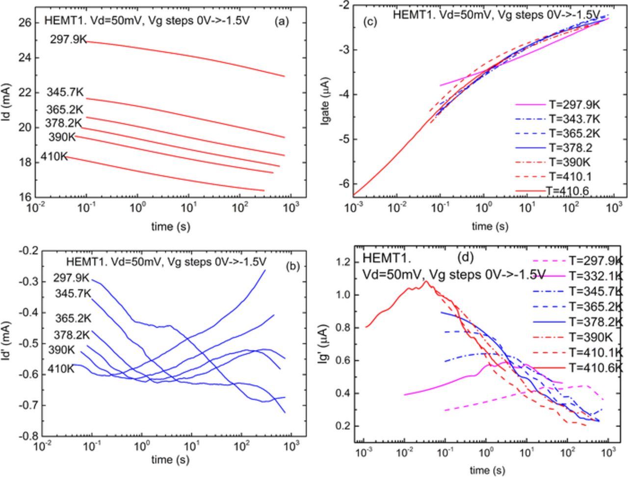
Figure 1. (a) Drain current relaxation curves measured for the gate voltage step 0 to −1.5 V for the HEMT1 structure at several temperatures; (b) derivatives of the drain current relaxation curves at several temperatures; (c) gate current relaxation curves of HEMT1 at several temperatures; (d) respective gate current derivatives.
The fitting with extended exponents is simpler. For all relaxations analyzed, good fits could be obtained assuming the presence of one major process with β ∼ 0.25 for HEMT1 and a minor process dependent on the height of the gate voltage step/pulse which becomes more pronounced when moving toward accumulation. The temperature dependences of the characteristic relaxation times of the main process are shown in Fig. 2. The activation energies of the gate and drain current relaxation times are similar and close to 0.7 eV. The drain current relaxation lags the gate current relaxation, as seen from Fig. 3 showing the derivatives of respective currents by logarithm of time at high temperature. This indicates the current transient in the drain current is due to the charge buildup in the AlGaN barrier and that the limiting stage is the charge movement and trapping with time in the barrier under the gate. The amount of trapped charge causing the steady-state decrease of the drain current is many orders of magnitude lower than the total amount of charge supplied by the steady-state reverse current at given temperature. The temperature dependence of the steady-state gate current in HEMT1 is insignificant compared to the temperature dependence of the gate current relaxation time during the capture process. This is illustrated by the temperature dependent I-V of the gate current in Fig. 4a. The activation energy of reverse current at low reverse voltage is only 0.1 eV, while for high reverse voltage close to the threshold voltage it is 0.065 eV. Such temperature dependence of the gate reverse current in AlGaN/GaN heterostructures is commonly observed in AlGaN/GaN HEMTs. The weak temperature dependence is often explained by the prevalence of direct tunneling of electrons into defect states with subsequent Pool-Frenkel assisted activation of the captured electrons into the band related to dislocations.12–14 It is not clear how this model can explain certain phenomena. For instance, the reverse current of HEMT1 at room temperature became much lower if the transistor was cooled down from high temperature at reverse voltage as compared to when it was cooled at 0 V or at forward voltage (compare I-V curves shown for cooling down from 470 K at −1 V and at +0.75 V in Fig. 4b).
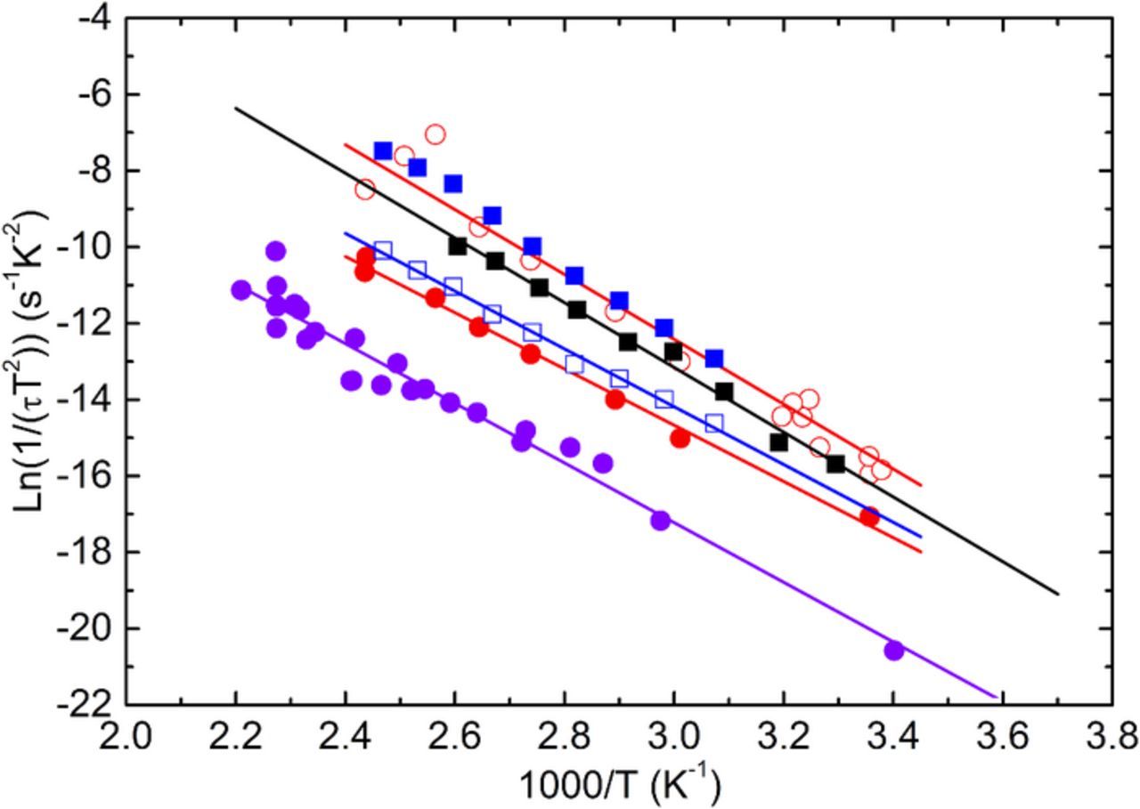
Figure 2. Arrhenius plots for HEMT current relaxation times; red circles-HEMT1, gate voltage step from 0 V to −1.5 V, open circles-gate relaxations, activation energy Ea = 0.73 eV, solid circles-drain relaxations, Ea = 0.64 eV; blue squares, HEMT1, steps from −2.1 V to −1.5 V, open squares-low temperature peak, Ea = 0.65 eV, solid squares-high temperature peak, Ea = 0.8 eV; violet solid circles-HEMT2, drain, 0 to −4 V steps, Ea = 0.68 eV; solid squares-taken for drain relaxations as measured by Joh and Alamo Ref. 6.
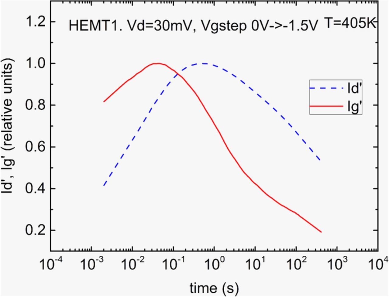
Figure 3. The derivatives of the gate current (solid curve, red) and drain current (dashed curve, blue) calculated from current relaxations of HEMT1 at 405 K, the data normalized to the peak values).
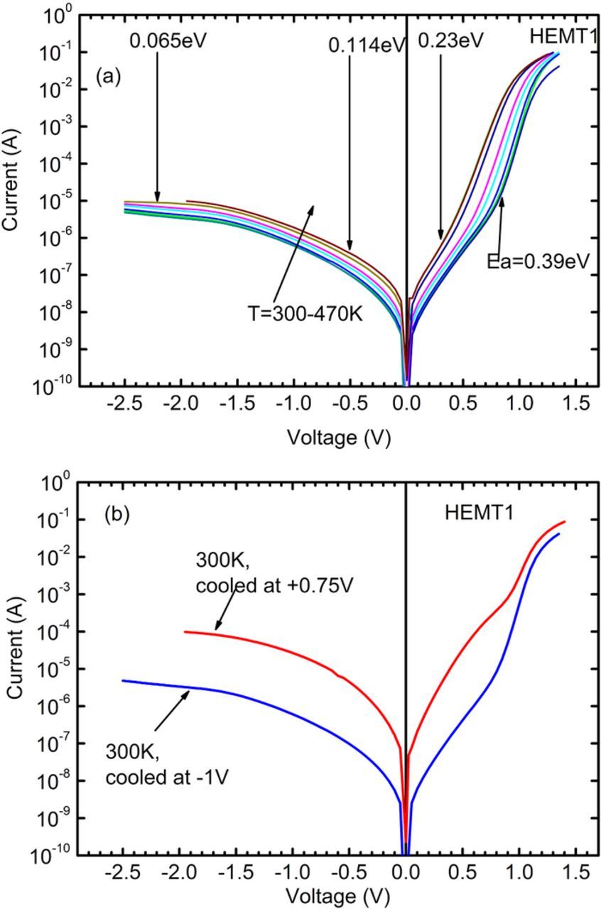
Figure 4. (a) Gate current I-V characteristics of HEMT1 measured at different temperatures; (b) Room temperature I-V characteristics measured after cooling from 470 K at −1 V (blue line) and +0.75 V (red line).
For transistors with high gate leakage, as in HEMT2, the threshold current could be moved to higher negative voltages by applying negative voltage pulse to the gate. This did not happen when positive voltage pulse was applied (Fig. 5). This means simple injection of electrons into the conduction band of the barriers by forward biasing the gate is not effective in building up the excessive negative charge driving electrons from the HEMT channel.
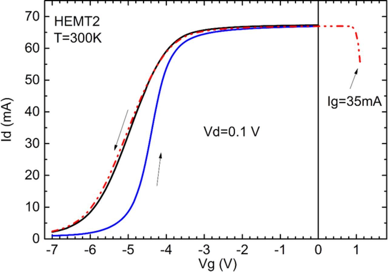
Figure 5. Room temperature drain current versus gate voltage I-V characteristics measured for the gate voltage swept from 0 V to −7 V (solid curve, black), from −7 V to 0 V (solid curve, blue), and from +1 V to −7 V (dashed curve, red); note the shift of the threshold voltage to lower negative voltage for sweeping from negative voltages and the lack of impact on threshold voltage of positive voltage application.
This data suggests that a step/pulse of high reverse voltage leads to direct tunneling of electrons into deep electron traps and thus increases the net negative charge locally. The captured charge can then hop from one deep trap to another in the direction of applied field by being thermally activated from the trap into the continuum of states, drifting along the field, and then being recaptured by another trap downstream. During all the time the reverse current is ON the supply of electrons trapped at the gate is replenished. In this way, a front of negative charge will be formed in the barrier and will move toward the AlGaN/GaN interface. The limiting stage in this hopping is most likely the thermal emission of electrons from the traps. Thus the measured activation energy will be close to the activation energy of emission. The effect of this negative charge on removal of electrons from the channel increases as the front approaches the interface. The fact that direct injection of electrons into the conduction band by forward biasing does not lead to the observed phenomena implies the presence of the capture barrier for trapping of the electrons directly from the conduction band, in contradiction with the proposed multistage emission/capture hopping proposed above. This can be resolved if one assumes the traps are localized above the Fermi level in a quantum-wire-like channel surrounded by a space charge region repulsing the bulk electrons present in the bulk conduction band. The movement of the charge along the quantum-wire-like channel occurs by the excitation of electrons from localized states to the sort of percolation level (the conduction band of the quantum wire).
The most suitable candidates for the role of such channels seem to be dislocations that are surrounded by space charge regions produced by deep acceptor states in the core (e.g. deep gallium vacancy related acceptors decorating dislocations).3 The barrier height can be substantial, so even at high temperatures, the electrons from the conduction band cannot penetrate the space charge region and be captured by deep traps. At the same time, electrons emitted from the deep traps to the continuum of states forming the conduction band along the dislocation wire can move along the wire until they are again captured by a deep trap. The electrons can be injected into the dislocation-related deep states easily by tunneling from the gate metal at high reverse voltage. These electrons can then be removed by illumination either directly, with sub-bandgap light, or by recombination with holes supplied by the intrinsic light. Clearly, at low temperatures the effect of illumination cannot be reversed by the application of forward bias. This naturally explains the often observed persistent changes in the threshold voltage of HEMT structures cooled under different gate voltages and illuminated at low temperatures.3,18 In this model one expects the characteristic relaxation time to vary slightly due to local potential fluctuations caused by fluctuations of composition, variations of electric field and local changes in strain. Consequently, when changing the length of the reverse gate voltage pulse one expects first to saturate the traps with the lowest barrier and hence the fastest relaxation time. Therefore, we expect the effective relaxation time to increase with the length of the gate voltage pulse, as is often the case with disordered systems described by extended exponents.19,20 This is experimentally observed for both HEMT structures studied here (see Fig. 6).
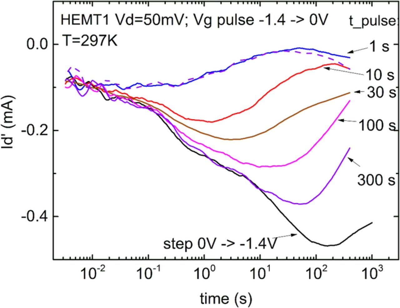
Figure 6. Drain current relaxation derivatives for different lengths of the gate voltage pulse (shown near respective lines).
The activation energies for capture are similar for the HEMT1 and HEMT2 structures. Moreover, the Arrhenius data for the capture process TP1 for the drain current transients taken from the work of Joh and Alamo6 also resembles the results for our transistors (Fig. 2). This suggests the traps are common and relate to an intrinsic or extrinsic state of dislocations.
One of the consequences of the proposed model is that one can observe in current or capacitance DLTS hole-trap-like signals (transient capacitance decreasing with time, drain current decreasing with time) caused by the presence of electron traps. This can be understood if one considers the Poisson equation with Nd+ donors and with Na deep acceptors with the level in the upper half of the bandgap. Before the application of the pulse/step, these acceptors are not charged and do not contribute to the space charge density which results in the starting space charge width W = Wo and starting capacitance Co ∼ 1/Wo. When the reverse bias step is applied and the acceptors start capturing electrons, a step is formed in the space charge and the front of this step moves toward the interface. As a result, the space charge density when the reverse voltage in DLTS is applied after the forward voltage pulse ends decreases, W increases and the capacitance decreases with time after the pulse as in the case of hole traps signal. This is illustrated schematically in Fig. 7 for the dependence of the space charge thickness W on the position of the step (x) moving with speed v = μE where μ is the effective mobility, E is electric field (also shown in Fig. 7). The calculations are shown for Nd = 1017 cm−3, Na = 2.5 × 1016 cm−3, the barrier height is taken as 1.5 eV. The calculations show that at small times (small x,) the space charge width (and capacitance) change slowly and the main effect is the change of the maximal electric field and hence the gate current. For longer times, when the step approaches the space charge edge, the change in W accelerates while the change in the electric field slows down. This is reflected in the drain current lag compared to the gate current in Fig. 3 because the change in the drain current follows more closely the change in capacitance. Depending on the length of the pulse, both electron-trap-like and hole-trap-like signals can be observed for the same electron trapping process, because of the movement of the space charge region boundary. Hole-trap-like signals are also often observed in standard DLTS or CDLTS measurements.9
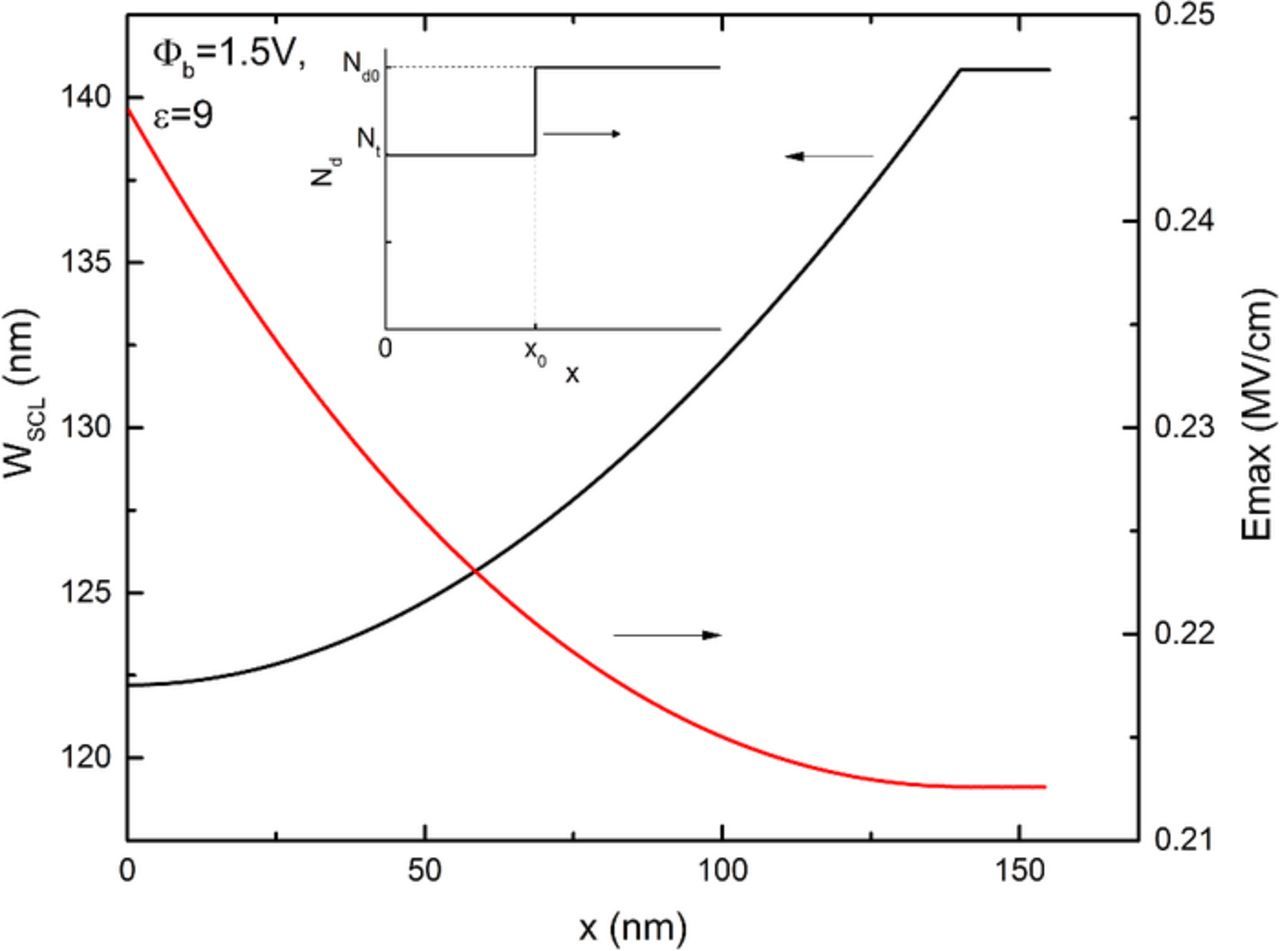
Figure 7. Schematic representation of the movement of the space charge step and related changes in the space charge region width and the maximum electric field.
The Arrhenius plots of these traps are similar to those observed in the capture experiments here and by Joh and Alamo6 (Fig. 8). Traps of the type described above manifest themselves not only in HEMT structures, but also in C-V profiles and DLTS signatures of single-layer n-AlGaN films when those contain surface regions with high doping and strong electric field comparable to the one encountered in HEMT barriers.
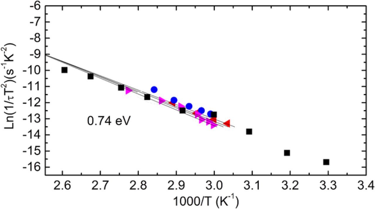
Figure 8. Arrhenius plots for the 0.74 eV electron trap in Ref. 6 (solid squares) and hole traps with similar signatures measured in another AlGaN/GaN on Si HEMT (all other symbols).
What is the nature of the reverse process of the drain current when turned on from the off state? Fig. 9 shows the drain current derivatives of the HEMT1 structure measured at different temperatures after applying the gate voltage step from −2.1 V (depleted channel) to −1.5 V (partly open channel). Two major steps are present, one with energy of 0.65 eV, the other with energy 0.8 eV, i.e. close to the activation energy of capture. The reverse process could consist in thermal emission from the deep states and hopping of emitted electrons in the direction opposite to the direction of capture. CDLTS measurements produced similar activation energy,9–11 but with a loss of detailed knowledge on the current relaxation waveforms.
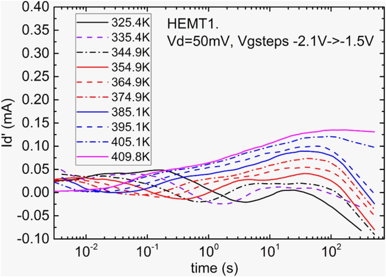
Figure 9. Derivatives of the drain current relaxations measured at various temperatures on HEMT1 after the application of the gate step from −2.1 V to −1.5 V.
Conclusions
The capture process leading to the gate current and drain current relaxation after the application of reverse voltage gate step/pulse in AlGaN/GaN HEMTs has activation energy ∼ 0.7 eV. This is explained by direct tunneling from the gate into empty electron traps and movement of the trapped charge toward the AlGaN/GaN interface by hopping via these deep traps by emission/drift/capture processes. Direct injection of electrons into the conduction band of AlGaN by forward gate voltage pulses does not initiate such a process, which means the presence of a barrier for capture of electrons directly from the conduction band of AlGaN. We suggest the trapped charge movement occurs via hopping along the quantum-wire-like states of dislocations surrounded by a high space-charge region. The hopping consists of capture of the electron from the gate on the deep state below the percolation level of the dislocations, thermal excitation from the trap to the percolation level of these dislocations, drift along the dislocations and re-capture by the deep trap. The reverse process occurring upon opening of the transistor channel consists of the charge front moving in the opposite direction, presumably via the same traps. These times become progressively longer with increasing pulse length, which requires appropriate measurements conditions in order to achieve reproducible results. The proposed model also explains the presence of hole-trap-like signatures in DLTS spectra of AlGaN/GaN structures without invoking recharging of the hole traps. We expect similar phenomena in AlGaN single layers under certain conditions. The results suggest that, in AlGaN/GaN structures with low dislocation density, fewer problems with gate-lag and with gate current leakage.
Acknowledgments
The work at NUST MISiS was supported in part by the Ministry of Education and Science of the Russian Federation in the framework of Increase Competitiveness Program of NUST «MISiS» (K2-2014-055). The work at UF was supported by DTRA 17-1-0011.