Abstract
We studied the growth of Si- and Sn-doped homoepitaxial β-Ga2O3 layers on (010)-oriented substrates by metal organic vapor phase epitaxy (MOVPE). At optimal growth conditions (850°C, 5 mbar) the layers were smooth with RMS roughness values of ∼600 pm. A microstructural study by transmission electron microscopy (TEM) revealed a very high crystalline perfection of the layers. No dislocations or planar defects were observed within the field of view of TEM. Using Si as dopant, the free electron concentration could be varied in a range between 1 × 10¹⁷ and 8 × 1019 cm−3, while with Sn the doping range was restricted to 4 × 10¹⁷−1 × 1019 cm−3. This was explained by a pronounced Sn memory effect in the MOVPE reactor that hampers achieving low carrier densities and by incorporation issues that limit the doping efficiency at high Sn doping levels. The electron mobility for a given doping density increased from ∼50 cm2/Vs for n = 8 × 1019 cm−3 to ∼130 cm2/Vs for n = 1 × 1017 cm−3 independently of the dopant. These values match the best literature data relative to β-Ga2O3 bulk crystals and layers grown by molecular beam epitaxy, setting a new standard for MOVPE-grown layers.
Export citation and abstract BibTeX RIS

This is an open access article distributed under the terms of the Creative Commons Attribution 4.0 License (CC BY, http://creativecommons.org/licenses/by/4.0/), which permits unrestricted reuse of the work in any medium, provided the original work is properly cited.
Transparent Oxide Semiconductors (TSOs) are an emerging class of materials, which combine high electrical conductivity with transparency down to the deep UV region.1,2 Among TSOs, monoclinic β-Ga2O3 is one of the most interesting compounds thanks to a wide bandgap (∼4.8 eV) that leads to a calculated electric breakdown field strength of 8 MV/cm.3,4 The most promising application of β-Ga2O3 is in the field of high power electronics, where it is predicted to outperform the leading technology based on SiC and GaN. A key advantage of β-Ga2O3 is that native substrates can be fabricated from bulk single crystals grown from the melt by Floating Zone (FZ),5 Edge-Defined Film Fed Growth (EFG)6 and Czochralski (CZ)7,8 methods.
The growth of homoepitaxial β-Ga2O3 has been mainly investigated by molecular beam epitaxy (MBE),9–11 and only rarely by metal organic vapor phase epitaxy (MOVPE).12–14 For both epitaxial techniques Schottky diodes and field-effect transistors have been realized.15,16 The structural quality of (100) β-Ga2O3 layers grown by MOVPE has been relatively poor so far, with maximum electron mobilities of ∼40 cm2/Vs,13 contrary to values achieved for layers grown by MBE on (010)-oriented substrates that are comparable to those of bulk material (>100 cm2/Vs).10 A further improvement of the growth of β-Ga2O3 by MOVPE is desirable, since MOVPE is more suitable for large-scale production.
Here we report on the MOVPE-growth of Si- and Sn-doped epitaxial β-Ga2O3 layers on (010) β-Ga2O3 substrates. We selected this substrate orientation to investigate whether it promotes the growth of layers with higher crystalline perfection. Moreover, thermal conductivity in β-Ga2O3 is anisotropic with the highest value along the [010] direction (27.0 W/mK at RT) and the lowest one along the [100] direction (10.9 W/mK at RT).17 Heat dissipation in devices fabricated on (010)-oriented substrates is then predicted to be almost three times more efficient, mitigating the main disadvantage of β-Ga2O3 compared to SiC and GaN that have much higher thermal conductivity.
The grown β-Ga2O3 layers were characterized by transmission electron microscopy (TEM) and Hall-effect techniques, revealing layers with a very high crystalline perfection and carrier mobilities close to the bulk β-Ga2O3 reference. The specific behavior of Si and Sn as dopants has been investigated. Sn-doping showed a significant memory effect in the MOVPE reactor and also incorporation issues in β-Ga2O3 for Sn concentration levels above 1019 cm−3. Si doping was more effective, leading to a wider doping range with a resulting free carrier concentration between 1 × 10¹⁷ and 8 × 1019 cm−3.
Experimental
β-Ga2O3 single layers were grown in a vertical shower-head low-pressure MOCVD reactor equipped with a rotating 3'' susceptor (Structured Materials Industries, Inc. - USA). Triethylgallium (TEGa), tetraethylorthosilicate (TEOS) and tetraethyltin (TESn) were used as metallorganic precursors for Ga, Si and Sn, respectively, while O2 was used as the oxygen source. High purity Ar, with a main flow rate of 1500 sccm, acted as carrier gas. The temperature of TEGa, TEOS and TESn bubblers was kept at 20°C, 5°C and −30°C, respectively. As substrates we used commercial semi-insulating (Fe-doped) (010) β-Ga2O3 substrates grown by the EFG method. Prior to growth, the substrates were cleaned with acetone and isopropanol, rinsed by de-ionized water, and dried with nitrogen flow. The growth experiments were mainly performed by applying the optimal experimental parameters used for the growth on (100)-oriented crystals, i.e. a susceptor temperature of 850°C, a reactor pressure of 5 mbar, TEGa and O2 molar flows of 6.0 × 10⁻⁶ and 2.2 × 10⁻² mol/min, respectively (standard growth conditions).13 The flow rates of TEOS and TESn were systematically varied in the range ∼1 × 10⁻¹¹–1 × 10⁻⁸ mol/min. All layers had thicknesses in the range 150–200 nm, as measured by spectroscopic ellipsometry (MM-16, Horiba Jobin Yvon). To provide contrast in the refractive index between layer and substrate we measured samples grown in parallel on sapphire and assumed that the growth rate is independent of the substrate. The surface morphology of β-Ga2O3 layers was studied by atomic force microscopy (AFM, Bruker Dimension Icon), while the structural properties were investigated by transmission electron microscopy (TEM, aberration corrected FEI Titan 80–300 operated at 300 kV). Secondary ion mass spectrometry (SIMS, at RTG Mikroanalyse GmbH) was used to determine the doping profiles and to get independent information on the thickness of homoepitaxial layers obtained by ellipsometry. Due to crater edge effects, the SIMS data near the surface (first 30–40 nm) is unreliable and omitted. We performed conductivity and Hall effect measurements at room temperature in van-der-Pauw configuration. Therefore, point-like contacts were prepared by applying InGa eutectic at the sample rim. The contacts showed ohmic behavior for all samples, except for those with dopant concentrations below 1017 cm−3 (preventing reliable Hall effect measurements).
Results
Epitaxial growth and structural characterization
By growing at the standard conditions of 850°C and 5 mbar, with TEGa and O2 flow rates of 6.0 × 10⁻⁶ and 2.2 × 10⁻² mol/min, the layers exhibited a flat surface with a mean roughness (RMS) of ∼600 pm, as shown in the AFM image of Figure 1a. The morphology was dominated by elongated islands oriented along the [001] direction. The growth rate, estimated from the resulting layer thickness and the growth time, was 2 nm/min, which is only 20% higher than that of layers grown on (100) substrates. This is in sharp contrast to published data for MBE growth reporting that growth rates on (010) surfaces are more than ten times higher than those on (100) substrates because of a higher re-evaporation rate of highly volatile Ga2O species from the (100) plane.10 To increase the growth rate we performed experiments with higher TEGa flows of 1.21 × 10⁻⁵ and 1.67 × 10⁻⁵ mol/min. The flux of O2 was adjusted to keep the Ga/O ratio constant. Figures 1b and 1c show that the roughness of the layers progressively increased, with RMS values of 1.25 and 11.4 nm. In the case of the intermediate TEGa flux (Figure 1b) the diffusion length of the adatoms on the β-Ga2O3 surface seems to be enhanced in the [100] direction, leading to larger islands. The growth rate increased to 3.4 nm/min. Figure 1c shows that a further increase of the Ga-precursor flow rate leads to very rough surfaces, characterized by well-defined crystallites that lose the directionality along the [001] direction. In this case the growth rate increased to 5.5 nm/min. For a given TEGa flow rate, different O2 flow rate in the range 5 × 10⁻³–3 × 10⁻² mol/min had no measurable influence on the layer growth. Doping generally did not affect the surface morphology of the layers. The only exception was the highest Sn-doped sample, grown with a TESn flow rate of 6.4 × 10⁻⁹ mol/min. Figure 1d shows that in this case the typical morphology of the layer is disturbed. The RMS roughness increases to 3.09 nm and the surface is characterized by elongated blocks ascribable to step-bunching. In another series of experiments, the growth temperature was decreased from 850°C to 700°C, while keeping the other parameters unchanged. The results, plotted in Figure 2, show a slight increase of the growth speed with decreasing susceptor temperatures. Since different flow rates of O2 did not alter this trend, the higher growth rate cannot be explained by a slower desorption of highly volatile Ga2O at lower temperatures, as proposed in the case of MBE growth.18 A higher oxygen partial pressure would indeed hinder the desorption of Ga suboxides. In our case, the growth at high temperatures is more probably limited by the desorption of Ga from the growing surface. To confirm this hypothesis, further investigation has to be carried out with the additional support of thermodynamic calculations.

Figure 1. AFM images of (010) β-Ga2O3 layers grown with (a-c) increasing TEGa flow rates of 6.0 × 10⁻⁶, 1.21 × 10⁻⁵, 1.67 × 10⁻⁵ mol/min with standard TEOS or TESn fluxes and (d) a standard TEGa flow rate of 6.0 × 10⁻⁶ mol/min and a high TESn flux of 6.4 × 10⁻⁹ mol/min.
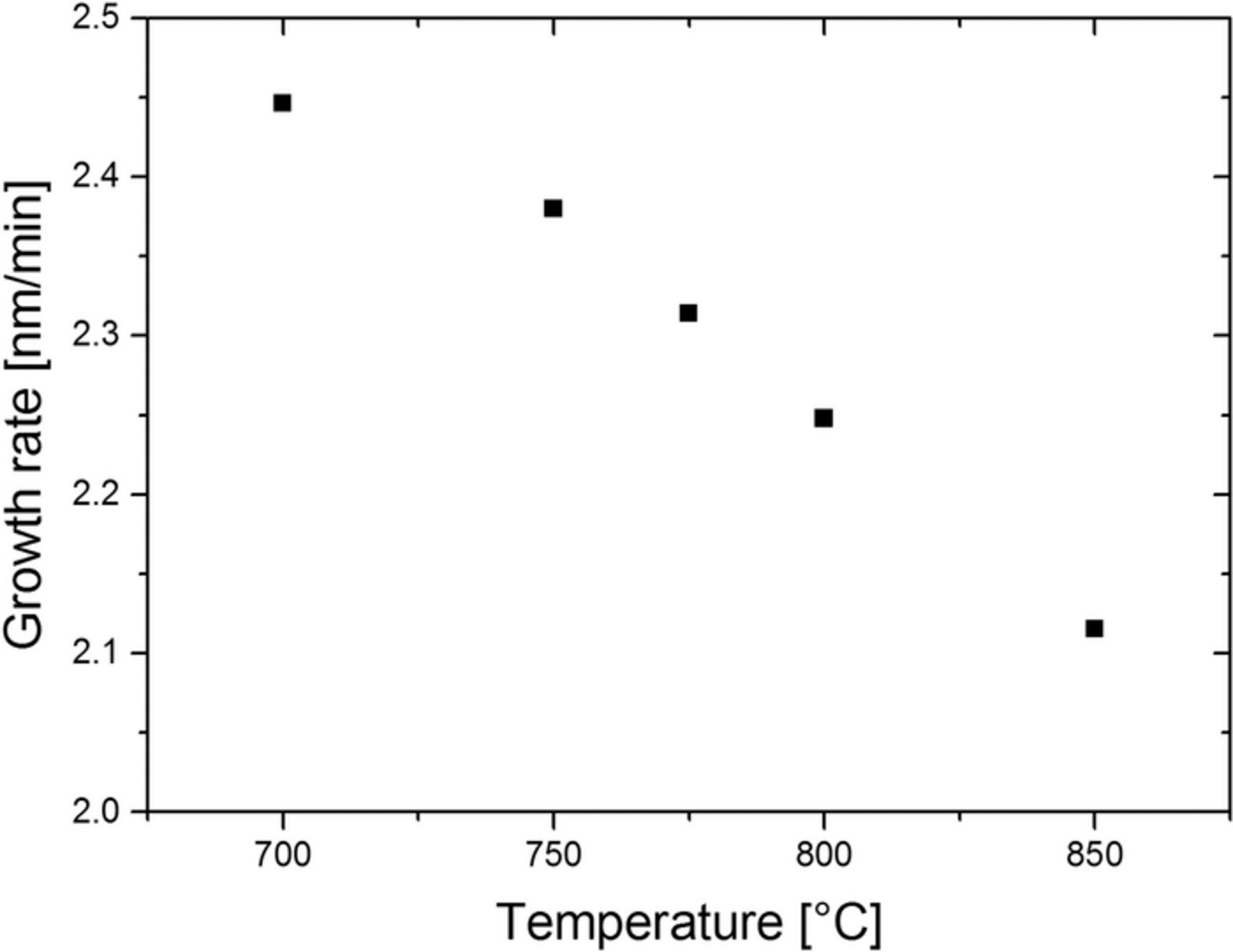
Figure 2. Dependence of the layer growth rate on the substrate temperature.
Figure 3 shows a representative cross-sectional bright-field image of a sample grown at standard growth conditions. The image was taken along the [201] direction, which corresponds to the surface normal of the a-plane. Within the field of view of transmission electron microscopy no extended defects such as planar defects or dislocations are present. More important, the interface between layer and substrate shows no measurable contrast.
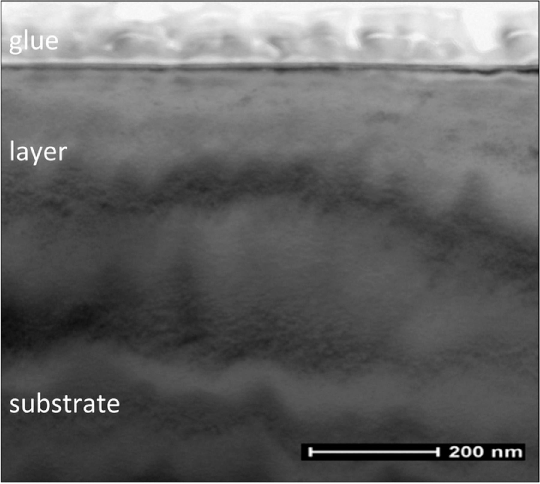
Figure 3. Typical bright field TEM image of (010) β-Ga2O3 layers showing the absence of planar defects.
Dopant incorporation
Figure 4 shows the SIMS depth profiles of the Si (a) and Sn (b) concentration obtained for TEOS and TESn flow rates varying in the range 3 × 10⁻¹²–6 × 10⁻⁹ mol/min and 0–6 × 10⁻⁹ mol/min, respectively. The doping concentration changes in the interval 5 × 10¹⁶–5 × 1019 cm−3 and 4 × 10¹⁷–1 × 1019 cm−3, respectively. For both dopants the doping profiles are mostly flat, pointing out a constant incorporation of the dopant species throughout the growth process. In Figure 4a a peak of the Si-signal with an intensity close to 1 × 1018 cm−3 is clearly visible at the interface between the substrate and the layer. A similar Si concentration was also observed in undoped and Sn-doped samples. Therefore, we conclude that it is most likely a contamination of the substrate surface that is present prior to growth of the layer. When comparing the profiles of low doped samples, it is obvious that the minimum dopant concentration in the case of Si-doping is as low as ∼5 × 1016 cm−3, while for Sn-doping the lowest achievable concentration is only ∼4 × 1017 cm−3. The latter value corresponds to a layer grown without TESn after a heavy doping experiment, pointing out a pronounced memory effect of Sn in the reactor. In the high doping region, the only atypical profile is relative to the highest Sn-doped sample. Here, a double-step feature indicates that the disturbed morphology shown in Figure 1d involves an irregular Sn incorporation.

Figure 4. SIMS depth profiles relative to Si (a) and Sn (b) in homoepitaxial (010) β-Ga2O3 layers grown with different TEOS (a) and TESn (b) flow rates.
The incorporation efficiency of Si from TEOS and of Sn from TESn is very similar, as can be deduced from the double-logarithmic plots of Figure 5. By increasing the amount of TEOS injected into the reactor by more than three orders of magnitude, from 2 × 10⁻¹² to 7 × 10⁻⁹ mol/min, the chemical concentration of Si in the layers increases nearly proportionally from 6 × 10¹⁶ to 6 × 1019 cm−3. In the case of Sn, the doping range is significantly reduced by the high Sn background level.
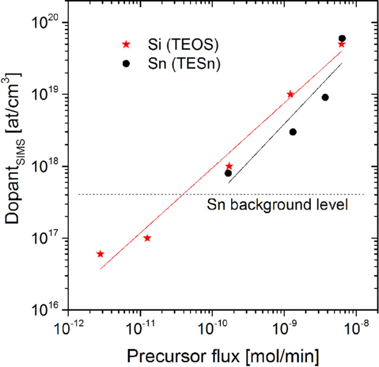
Figure 5. SIMS concentration of Si (red stars) and Sn (black circles) versus TEOS and TESn flux. The solid lines are the linear regression of the experimental data, the dashed one indicates the Sn background level due to memory effect.
Electrical characterization
In Figure 6, the free electron concentration n is displayed vs. the chemical Si and Sn concentration as measured by SIMS. For both dopant species, the free carrier density increases linearly with the dopant concentration, pointing to negligible compensation as well as effective incorporation of the dopants in electrically active sites. The only exception to this trend is the layer doped with the highest Sn concentration that shows a carrier density of 3 × 1018 cm−3, despite a Sn incorporation of 6 × 1019 cm−3.
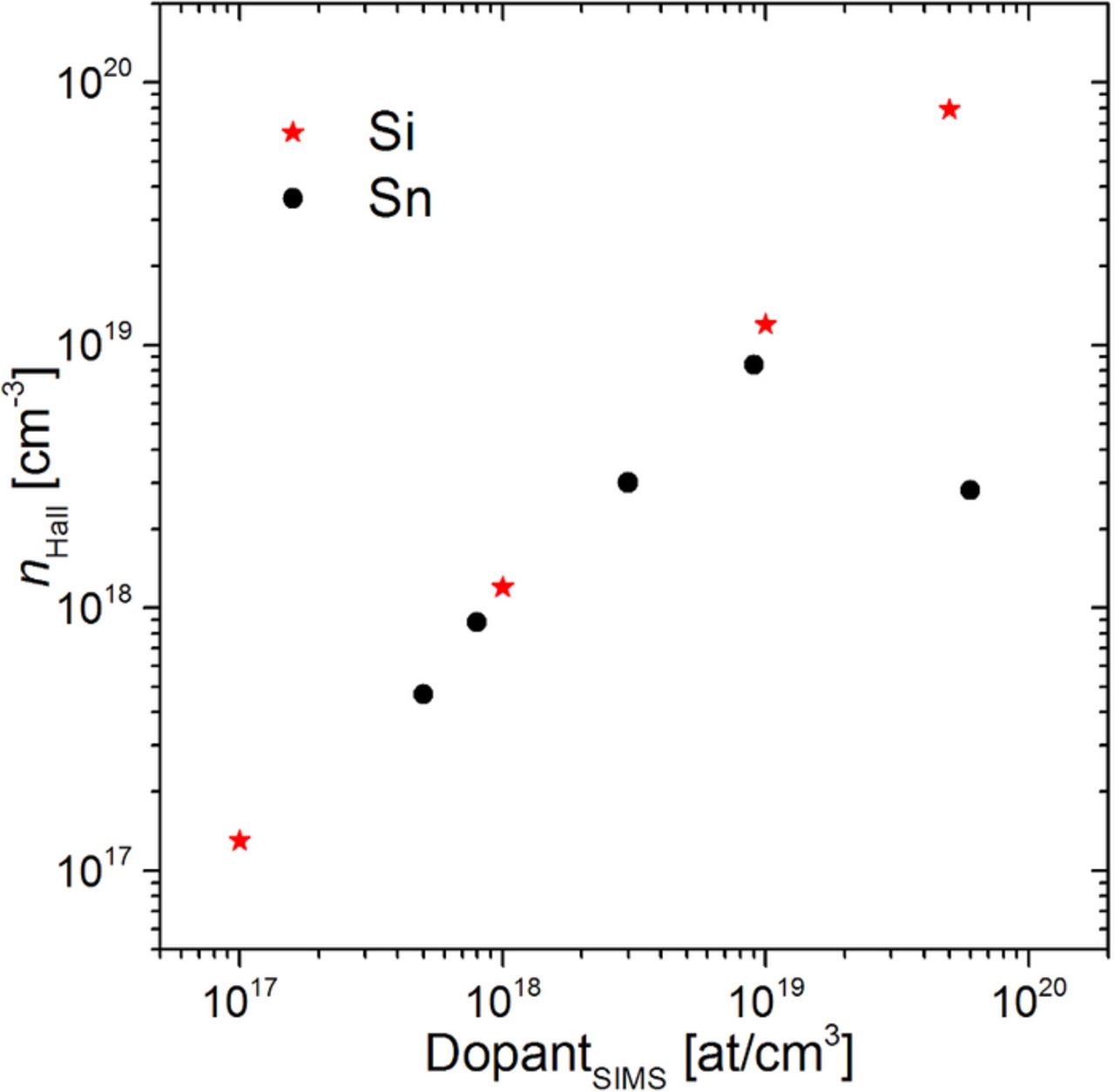
Figure 6. Hall free carrier concentration versus the dopant (Si and Sn) concentration obtained by SIMS.
Figure 7 shows the Hall mobility μ as a function of the free carrier concentration for Si- and Sn-doped layers. The electron mobility increases with decreasing free carrier density, spanning from ∼50 cm2/Vs at n = 8 × 1019 cm−3 to ∼130 cm2/Vs at n = 1 × 1017 cm−3. Such a mobility behavior indicates that scattering at ionized impurities dominates. The mobility values are slightly higher than those of MBE-grown layers and bulk crystals reported in Ref. 10, confirming the high crystalline perfection of the MOVPE layers. An exception is once more the layer with the highest Sn-doping level, where the mobility is reduced to 32 cm2/Vs (not shown in Figure 7).
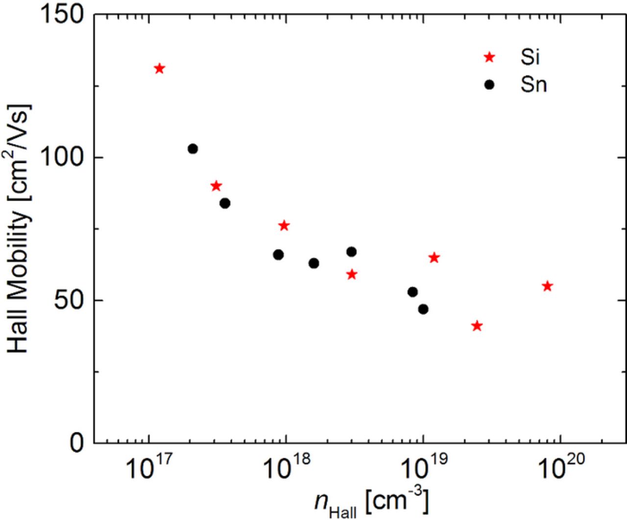
Figure 7. Hall mobility values as a function of carrier density for Si- and Sn-doped layers.
Discussion
The excellent structural and electrical properties of the layers shown in the previous paragraphs are closely related to the crystal orientation of the substrates. (010) β-Ga2O3 substrates were specifically selected to improve the results that we previously obtained for (100)-oriented layers, whose properties were strongly affected by planar defects, in particular stacking faults and twins. These were caused by the nucleation on the β-Ga2O3 (100) surface of 2D islands with two different orientations, mutually rotated by 180° on the a plane, by a mechanism known as double positioning.13 The choice of an alternative substrate orientation was successful, since TEM investigation showed no planar defects in (010)-oriented layers, pointing out that double positioning does not occur on the β-Ga2O3 (010) surface.
The different doping behavior of Si and Sn in the low and high doping regimes described in the previous paragraphs is discussed in the following.
The residual Sn contamination observed in low-doped layers grown after high Sn-doping runs is not cited in the literature, where the most reported memory effect in MOVPE is relative to Mg in p-doped AlGaN/GaN layers.19,20 Since similar flow rates of TESn and TEOS lead to a comparable incorporation of Sn and Si in the layers (see Figure 5), we can assume that both precursors have a similar decomposition efficiency and that a comparable amount of free Sn and Si atoms are present in the reaction atmosphere. A large part of these is supposed to be incorporated in the layers, but unreacted Si and Sn atoms are pushed by the carrier gas to the exhaust system. However, since Sn is much heavier than Si, there is a higher probability that Sn atoms are not efficiently expelled, but stick on the walls of the reactor or on the surface of the showerhead. Although these parts are liquid cooled to limit the desorption of material during the growths, the higher vapor pressure of Sn compared to Si makes the re-evaporation of Sn a potential source of contamination for the β-Ga2O3 layers. In order to minimize the memory effect, after each high Sn doping experiment special cleaning runs were performed in high O2 flux at 850°C with a reduced reactor pressure of 3 mbar. Nevertheless, a significant decrease of the basic Sn contamination was not observed, making it necessary to develop better cleaning procedures to improve the growth of layers with lower doping levels. Further investigation is planned to find a suitable solution.
In the high doping range, while Si-doping showed a regular dopant incorporation without significantly affecting the growth, Sn concentrations higher than 1 × 1019 cm−3 altered the properties of β-Ga2O3 layers. Figure 1d and the relative SIMS profile in Figure 4b show that a Sn-incorporation of ∼6 × 1019 cm−3 is high enough to hinder a coherent dopant incorporation and influence the growth mechanism, leading to the formation of well-defined oriented blocks. The electrical properties of the layer are affected as well. The reduced free carrier concentration of 3 × 1018 cm−3 (Figure 6) indicates a much lower doping efficiency in comparison to the other samples. This result can be explained by a lower ratio of Sn atoms in electrically active position and by the formation of complexes and extended defects that compensate the Sn donors and limit the electron transport properties of the material. The second mechanism is supported by the reduced mobility value of 32 cm2/Vs measured for the same layer. The more straightforward incorporation of high Si concentrations in β-Ga2O3 layers in comparison to Sn can be intuitively understood by comparing the formation energies of the relative substitutional defects reported by Varley et al.21 Here, the authors calculated by means of density functional theory (DFT) the preferential lattice positions and the formation energies Ef for several shallow donors impurities in β-Ga2O3. As an outcome of this study, Si results to prefer the tetrahedral coordination of the Ga(I) site, while Sn the octrahedral coordination of the Ga(II) site. The probability that Si or Sn substitute Ga atoms varies for different experimental growth conditions. In an oxygen-rich regime, the formation energy of SiGa(I) and SnGa(II) is substantially the same, while Si has a significantly lower formation energy (ΔEf ∼ 0.65 eV) in an oxygen-poor regime. Although in our experiments we use much higher O2 flow rates than those of TEGa, the electrical characterization of the layers indicates that the growth conditions are actually closer to an oxygen-poor (Ga-rich) regime, as intended in Ref. 21, since this hinders the formation of gallium vacancies (VGa), which are the main compensating species in β-Ga2O3.22 A high VGa concentration would indeed limit the doping efficiency of the layers, which is instead close to 100% (Figure 6). The lower formation energy of the relative substitutional defect makes the limit for the incorporation of Si in electrically active sites higher than that of Sn, which in our case is close to a Sn concentration of ∼1 × 1019 cm−3. Beyond this threshold, the incorporation of the dopant affects the growth of the layers and, consequently, their properties.
Conclusions
The growth of semiconducting (010) β-Ga2O3 homoepitaxial layers by MOVPE was successfully carried out by using Si and Sn as dopants. No additional dislocations or planar defects were observed within the field of view of TEM. Si and Sn presented peculiar differences in the doping of the layers. With Si it was possible to tune the free carrier density between 1 × 10¹⁷ and 8 × 1019 cm−3 by appropriate adjustment of the relative precursor flow rate. The use of Sn was not so straightforward and the extension of the effective doping resulted to be limited to 4 × 10¹⁷–1 × 1019 cm−3. The lower end of this range was determined by a pronounced memory effect of Sn in the MOVPE reactor, while the higher one by the incoherent incorporation of Sn in the β-Ga2O3 matrix that affected the crystallinity of the layers and, consequently, the doping efficiency. The electron mobility for a given n-value was identical for both dopants and increased from ∼50 cm2/Vs up to ∼130 cm2/Vs for decreasing doping levels, establishing a new record for layers grown by MOVPE.
Acknowledgments
The authors thank Z. Galazka and D. Klimm for fruitful and stimulating discussions and R. Grüneberg for technical assistance during the growths.