
Abstract
Thin-film lithium-ion batteries (LIBs) have attracted much attention as one of the state-of-the-art energy storage technologies. However, most research regarded the current collector as infinitely conductive or with no separate simulation for this part. Herein, a model is proposed to simulate thin-film current collectors' potential distribution and resistance. The effects of changing the aspect ratio and the thickness on the thin-film current collector are investigated. The experimental results obtained are in excellent agreement with the model. At the same time, this method is quite generic and can also be used for other types of batteries.
Export citation and abstract BibTeX RIS

This is an open access article distributed under the terms of the Creative Commons Attribution 4.0 License (CC BY, http://creativecommons.org/licenses/by/4.0/), which permits unrestricted reuse of the work in any medium, provided the original work is properly cited.
Consumption of fossil fuels and environmental issues result in attention to clean energy, including storage, conversion, and energy usage. LIBs have become the most important power source for electronics and electric vehicles due to several advantages, such as high energy density, long cycle life, environmental friendliness, 1,2 etc. As a vital part of LIBs, the current collector supports electrode materials and transfers electrons between the active material and the external circuit. 3–5 In order to avoid electrochemical corrosion of the current collector, aluminum foils and copper foils are generally used as the current collectors for the cathode and anode, respectively. 6,7
However, research on LIBs focuses on improving cathode materials and electrolytes, with little focus on the current collector. Current collectors were always regarded as infinitely conductive, and the electronic part of especially thin-film LIBs was ignored. Besides, the resistance of the current collector was usually counted in the total ohmic resistance or contact resistance and has not been simulated separately. 8–16 In particular, few studies have been conducted on modeling thin-film current collectors, which is important for thin-film LIBs since the resistance of the current collector can cause abrupt voltage change and potential differences in batteries then, resulting in polarization and affecting battery operation. 17–20 Its resistance can also obviously impact the current density distribution and the utilization of materials of batteries, which is a topic of ongoing investigation. Therefore, studying the current collector's resistance is necessary and significant. Frequently, commercial software does not provide all the correct technical details that can be used for LIBs models. This gap should be filled.
Herein, we build a model to calculate the resistance of arbitrary thin-film current collectors for thin-film batteries. The classical 3D Laplace equation showing the potential distribution in a flat slab is converted to the 2D Poisson equation for the thin film. The corresponding transformation and the link between the parameters of the 3D equation (resistivity and geometrical dimensions) with the parameters of the 2D equations (sheet resistance) are first proposed. Derivation presumes that the thin film's thickness is small compared to other dimensions. Several numerical examples are considered. The derivations proposed by us about the resistance of the thin-film current collector and modeling the electronic currents are beneficial for improving the existing thin-film lithium-ion battery models. 11,21,22 The experimental data were collected by a four-point probe device and compared with the model prediction. The presented approach is quite generic and can be applied and expanded to other types of LIBs.
Theoretical
Consider the layout for the current distribution calculation. Figure 1 shows a thin-film current collector F with geometrical dimensions L (length), W (width), and H (thickness). Assume that current is supplied to the thin film through two geometrical places at the top, denoted as  and
and  as shown in Fig. 1. C1 and C2
are two-dimensional projections of
as shown in Fig. 1. C1 and C2
are two-dimensional projections of  and
and  onto the xy-plane (i.e., z = 0).

Figure 1. (a) Scheme of thin-film solid-state batteries (b) Layout for the current distribution calculation of the current collector. The blue arrows indicate the direction of electrons.
Download figure:
Standard image High-resolution imageThe current density J [A m−2] inside the current collector should be non-divergent, that is

According to the differential form of Ohm's law

where  [V] is the potential function and ρ [Ohm m] is the material's resistivity. Combining the Eqs. 1 and 2 when the resistivity is constant, resulting in

Furthermore, Eq. 3 also can be written in standard form

Consider the boundary conditions of Eq. 4. Denote the boundary of the thin-film current collector as  Then current density J must be equal to zero for all points on
  except
  and
and  regions. According to Eq. 2, that can be written as

where the derivative is taken with respect to the outer normal vector. Assume that current I [A] is supplied to the thin-film current collector via the area  which has a surface area A [m2]. Then the absolute magnitude of the current density is I/A [A m−2]. The corresponding flux is directed orthogonally to the surface. Therefore, combined with Eq. 2, the answer should be

Similarly, assume that output current I passes via the area  which has the same surface area as
  Then the boundary condition related to
  can be obtained with the apparent change in the sign

Then assume that the thickness of the thin-film current collector is small enough compared with the length and width so that the potential does not change too much across the thickness. Thus, the z dimension can be reduced by considering averaging across it.

Equation 8 defines  which is the average of the 3D potential
  with respect to film thickness. Based on Eq. 4, it could be written as
Integrating Eq. 9 gives
According to Eqs. 5-7, the derivative  is always equal to zero. However,
  can be different from zero when (x,y,H) belongs to the area
  or
or  Therefore, Eq. 10 can be written as

where the function  is defined as
Then the potential distribution can be obtained by solving Poisson's Eq. 11 with zero flux at the boundaries. In addition, the Neumann boundary condition is considered. At the border, the equation is

This boundary problem is discretized, and finite difference equations are derived. 23 This approach is programmed in Matlab. The least-squares solution is obtained, and the potential distribution on the thin-film current collector is finally found.
Results and Discussion
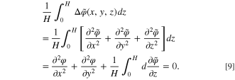
Figure 2 demonstrates the potential distribution of a 100 nm thick copper current collector (3 × 1 cm). The input and output currents are supplied via two small areas (tabs) located on the opposite sides of the strip at a distance of 0.25 cm from the edges. The bumps shown in Fig. 2a represent the current input and output positions (corresponding to  and
and  area in Fig. 1b). The position of the currents can be arbitrarily changed to obtain the potential difference between any two points. The blue arrows in Fig. 2b demonstrate the current density.
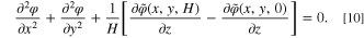
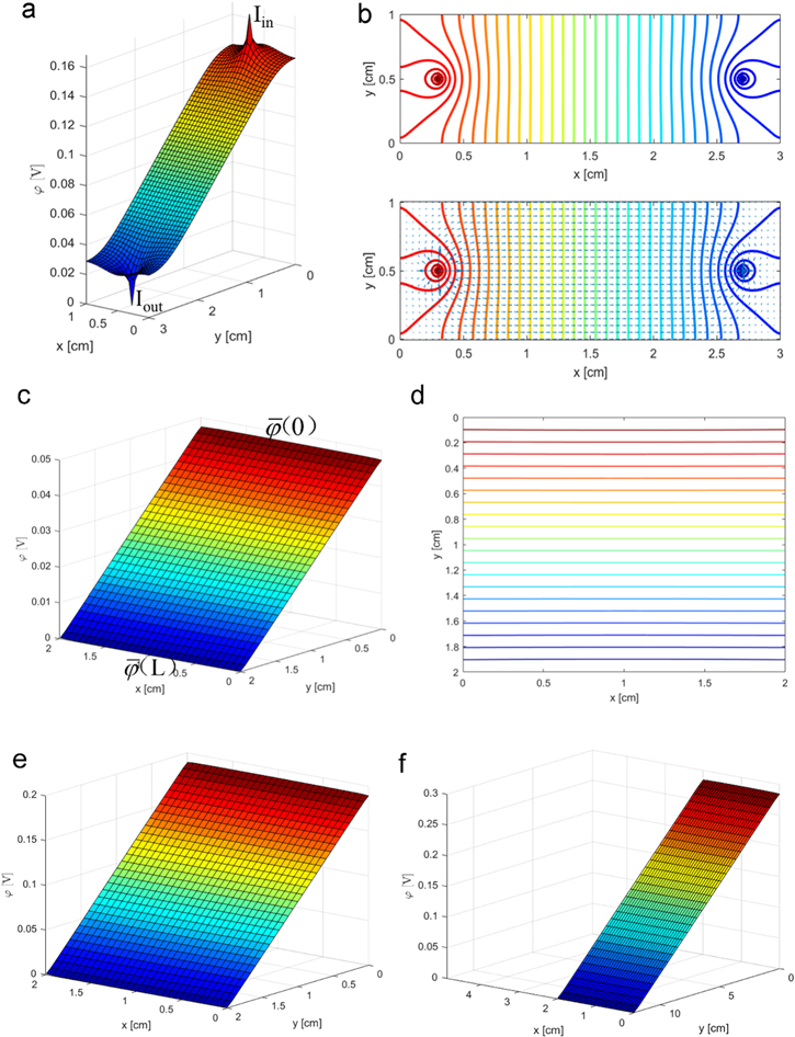
Figure 2. (a) Potential distribution in the rectangular current collector and (b) corresponding contour plot. (c) Potential distribution of the current collector when currents are supplied through the entire edge and (d) corresponding contour plot. Potential distribution of the thin-film current collector after (e) decreasing the thickness and (f) enlarging the aspect ratio.
Download figure:
Standard image High-resolution image
Another illustration relates to the definition of sheet resistance. It is commonly accepted that if the current is applied to edges, the resistance of a square thin film does not depend on the dimension but is only related to the thickness. That is, actually, the definition of sheet resistance. Therefore, simulating this situation in the present approach is also interesting. Figure 2c and Figure 2d show the potential distribution when currents are supplied through the whole edge of the current collector. The potential distribution in Fig. 2c is linear, in good agreement with the parallel contour lines in Fig. 2d. The sheet resistance can be calculated according to Eqs. 14 and 15. Averaging the potential at the edges of the current collector across the x coordinate leads to

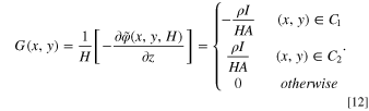
Then the sheet resistance is the difference between the average potentials at two edges divided by the current, according to

Rephrasing, the resistance of a square thin-film material in the direction of current is the sheet resistance. According to the modeling results, the sheet resistance of the 80 nm thick thin-film current collector is 0.47 Ω no matter the dimension is from 1 × 1 cm to 5 × 5 cm, which eventually points to the model's reliability. Moreover, the voltage drop across the current collector can be observed, which might produce polarization and affects battery operation. The voltage drop would be more noticeable when the aspect ratio of the current collector is large or when the current is high. Figure 2e demonstrates the potential distribution of the thin-film current collector after decreasing the thickness, which indicates a larger potential drop and resistance. Changing dimensions or aspect ratios of the thin-film current collector can lead to similar conclusions, as shown in Fig. 2f. It is easily found that the voltage drop is 4–6 times larger compared to the original. This greater voltage drop can lead to an uneven distribution of current density as well as affect the utilization of electrode materials of batteries, thus affecting the cyclic life.
Copper thin films with different thicknesses have been prepared by physical vapor deposition (PVD) to validate this model. Silicon wafers were used as substrate. The deposition method was thermal evaporation, with a deposition speed of 1 Å/s. Substrates kept rotating at a speed of 20 rpm to guarantee homogeneous deposition. After deposition, 80, 240, and 400 nm thick copper films were obtained. A profilometer (Bruker, USA) and scanning electron microscopy (FEI, USA) were used to verify the thickness of the samples. Figure S1 shows SEM images of the copper thin-film samples with different thicknesses. The sheet resistances were tested using a four-point probe device (Ossila, the UK) shown in Fig. S2. All results are listed in Table I. The error between experimental and simulated values is no more than 2%, which proves that the proposed model is highly reliable.
Table I. Sheet Resistance of Cu thin film.
| Thickness/nm | 80 ± 2 | 240 ± 3 | 400 ± 5 |
| Experimental values/Ω | 0.479 | 0.112 | 0.057 |
| Simulated values/Ω | 0.471 | 0.113 | 0.058 |
| Error/% | 1.67 | 0.89 | 1.75 |
Moreover, the resistance across a larger range of thicknesses used in most batteries today is calculated based on our model. It can be seen from Table SI that the different thicknesses can bring huge differences in sheet resistance of several orders of magnitude. This difference is most noticeable especially when the thickness of the current collector is reduced to an ultra-thin thickness of around 10 nm. In addition, the deposition conditions, temperature, and the nature of the Cu to substrate bonding influence the structural behavior and film density, thus further affecting the resistance of the thin-film current collector. On the other hand, the resistances of different materials are also studied. As listed in Table SII, the sheet resistance of Li foil is around five times more than Cu foil. Consequently, it might cause more severe voltage drop and power loss in thin film batteries that don't use a separate current collector for the anode but directly use Li metal.
Based on the above results, it can be concluded that the thinner thickness of the current collector and larger aspect ratio result in larger resistance, which further affects the current distribution and leads to energy and power losses. Therefore, the size and the preparation method of the thin-film current collector should be designed with a combination of cost and performance in mind.
Conclusions
A model to simulate the resistance of thin-film current collectors has been developed, which allows the calculation of the resistance between any two points on the thin-film current collectors. The model can also calculate the thin film's sheet resistance with arbitrary dimensions. The effect of the current collectors' dimension and resistance on the potential distribution is illustrated. The method is quite generic and can also be applied to other current collectors. A four-point probe device was used to test the sheet resistance of the investigated current collector. The experimental findings are in excellent agreement with the modeling results. This model is instructive for further investigating the electronic components of lithium-ion batteries and improving existing lithium-ion battery models.
Acknowledgments
The author Z. Wang gratefully acknowledges fellowship support by the China Scholarship Council.
Supplementary data (1.2 MB DOCX)