
Abstract
The roles of zinc and nitrate ions in the electrochemical growth of ZnO were examined in this study. ZnO was deposited on a polycrystalline Cu substrate from electrolyte containing 0.0025–0.08 M zinc nitrate and 0.1–2.0 M potassium nitrate. The morphology, epitaxial orientation relationship, interfacial microstructure, and photoluminescence (PL) properties of the ZnO deposits were characterized. The ZnO morphology was found to be controlled mostly by the zinc ion concentration in the electrolyte. Here, 50–400 nm wide hexagonal pillars were deposited from electrolyte with potassium nitrate concentration as high as 0.4 M. All the deposited films had strong 〈0001〉//ND fibre texture. Most of the ZnO crystallites were grown epitaxially on Cu grains regardless of the electrolyte concentration. The major epitaxial orientation relationship was identified as (0001)ZnO//(103)Cu and [11 0]ZnO//[010]Cu, and three other epitaxial orientation relationships were also identified. Samples consisting of nanopillars or plates exhibited excellent PL characteristics with near bandgap–deep level emission intensity ratios of 2.4–4.3 and full width at half maximum of the NBE peak of 122–131 meV.
Export citation and abstract BibTeX RIS

This is an open access article distributed under the terms of the Creative Commons Attribution 4.0 License (CC BY, http://creativecommons.org/licenses/by/4.0/), which permits unrestricted reuse of the work in any medium, provided the original work is properly cited.
Zinc oxide (ZnO) films have attracted considerable attention for their possible applications in solar cells, transparent conducting electrodes, photodetectors, and ultraviolet light emitting devices. 1 Some applications require ZnO films strictly in the epitaxial form, whereas polycrystalline films are acceptable in others. Polycrystalline films are used as a compromise typically because of the difficulty of growing epitaxial films with high crystalline quality. ZnO epilayers can be prepared using various methods, such as chemical vapour deposition, pulsed laser deposition, and molecular beam epitaxy, 2–4 most of which require a high-vacuum environment and high temperature. In 1996, two research groups separately reported that ZnO could be deposited electrochemically in nitrate and chloride electrolytes. 5–7 Following the pioneering study of Izaki and Omi, 5,6 scholars revealed that the concentration of zinc nitrate in the electrolyte considerably affects the morphology of the deposited ZnO crystals. 8–10
The electrodeposition process of ZnO in a nitrate electrolyte consists of the following stepwise reactions 6


The reduction reaction in (1) allows the production of hydroxyl ions at the electrode surface, 11 which increases the local pH and allows reaction (2) to proceed. The zinc ions absorbed on the electrode surface function as a catalyst for the charge transfer process, and the generated hydroxyl ions can react immediately with the zinc ions to form zinc hydroxide or ZnO. 8 Reaction (1) is therefore a crucial step in ZnO deposition, and the concentrations of both zinc and nitrate ions should affect this reaction in different aspects. Typically, well-oriented hexagonal pillars of approximately 100 nm or less in diameter are obtained at low Zn2+ concentrations (0.0001 to 0.01 M), whereas irregular nanoparticles or hexagonal plates are deposited at zinc ion concentrations higher than 0.01 M. 9,10,12 Moreover, Izaki and Omi revealed that the concentration of Zn(NO3)2 cannot exceed 0.2 M if almost stoichiometric ZnO is required. 6 Furthermore, the morphology of the ZnO crystals is sensitive to the chloride concentration. 13,14 Decreasing the deposition potential and increasing the electrolyte temperature promotes the deposition of nanopillars. 10 Bai et al. attempted to distinguish the effects of zinc and nitrate ions on ZnO morphology and concluded that thicker pillars were deposited at higher concentration of either ion. 15
Most studies have focused on the formation of one-dimensional ZnO nanostructures in a dilute electrolyte. The effect of zinc and nitrate ions, in a wide concentration regime, on morphology evolution has not yet been extensively investigated. A few studies have demonstrated that ZnO epilayers or epitaxial nanopillars could be grown on single crystal substrates such as GaN/sapphire, Au, and Pt. 16–19 The preliminary results suggest that the low-cost process is feasible to deposit ZnO epilayers. In this study, systematic experiments were conducted to investigate the effect of electrolyte concentrations of zinc ions and nitrate ions on the morphology, preferred orientation, and crystallinity of the ZnO crystallites. Special emphasis was placed on exploring the feasibility of growing ZnO epitaxial films or nanopillars on Cu substrate by using the electrochemical method. Deposits were characterized through X-ray diffraction (XRD), scanning electron microscopy (SEM) and photoluminescence (PL) spectroscopy. The epitaxial orientation relationship between ZnO and Cu and the ZnO–Cu interface were investigated through electron backscatter diffraction (EBSD) and transmission electron microscopy (TEM).
Experimental
ZnO was electrochemically deposited in electrolyte containing reagent grade Zn(NO3)2·6H2O (≥99% in purity) and KNO3 (≥99% in purity). Deionized water purified by a Milli-Q system was employed, and the pH of the electrolyte was adjusted to 6 by using KOH. Cathodic deposition was conducted at 353 K by using a three-electrode configuration under a galvanostatic condition (0.1 mA cm−2, Autolab PGSTAT 204) with an Ag/AgCl reference electrode and a Zn plate as a counter electrode without stirring. The working electrode was a polycrystalline Cu substrate of 1 × 1 cm2 in size. The Cu substrate was cut from a 1-mm-thick cold rolled sheet (99.8 wt% pure) and annealed at 1073 K for 3600 s in air. The annealed substrate was then ground using SiC paper to remove the surface oxide layer and electropolished prior to the deposition. The electropolishing parameters and surface morphology and roughness of Cu grains in various orientations have been reported elsewhere. 20 Two series of electrodeposition experiments were conducted. First, the zinc nitrate concentration in the electrolyte, containing 0.4 M potassium nitrate, was varied from 0.0025 to 0.08 M. Second, the potassium nitrate concentration was varied from 0.1 to 2.0 M for a fixed zinc nitrate concentration of 0.02 M. Table I displays the sample designations and corresponding electrolyte concentrations.
Table I. Deposited samples and the corresponding electrolyte concentrations.
| Sample | Zn(NO3)2, M | KNO3, M | [NO3 −], M | [Zn2+]/[NO3 −], ×10−3 |
|---|---|---|---|---|
| Z03K04 | 0.0025 | 0.4 | 0.405 | 6 |
| Z05K04 | 0.005 | 0.4 | 0.41 | 12 |
| Z20K04 | 0.02 | 0.4 | 0.44 | 45 |
| Z80K04 | 0.08 | 0.4 | 0.56 | 143 |
| Z20K01 | 0.02 | 0.1 | 0.14 | 143 |
| Z20K08 | 0.02 | 0.8 | 0.84 | 24 |
| Z20K13 | 0.02 | 1.3 | 1.34 | 15 |
| Z20K20 | 0.02 | 2.0 | 2.04 | 10 |
The crystal structure and preferred orientation of the deposited films were characterized by XRD (Bruker D8 Discover with Cu Kα radiation). The surface morphology was observed through SEM (Zeiss Supra 55, operated at 5 kV). The scanning electron microscope was equipped with an EBSD detector (Oxford symmetry). The orientation image maps (OIMs) of the Cu substrate and deposited film for the same position were analyzed through EBSD with a step size of 1 μm. Additional EBSD analyses for cross-sectional samples were performed. A right-handed Cartesian coordinate system consisting of three orthogonal axes: RD (x), TD (y) and ND (z) was used to define the sample orientation. Here ND represents for the normal direction of the grain/film surface and the axes RD and TD were parallel to the two sides of the sample, respectively. The samples were polished using a Leica EM TIC-3X ion polisher. Cross-sectional samples for TEM analyses were prepared using the focused ion beam technique. PL spectra were acquired at room temperature using a Horiba HR 800 spectrometer equipped with a 325 nm He-Cd laser as the excitation source. To comprehensively understand the luminescent characteristic, each sample was measured at 5–10 positions.
Results
Effect of the zinc ion concentration on the morphology, epitaxial growth, and PL properties of ZnO films
In this section, the results obtained from four samples, Z03K04, Z05K04, Z20K04, and Z80K04 are discussed. Figure 1 shows the XRD patterns for samples deposited from electrolyte containing 0.0025 to 0.08 M zinc ions. In addition to the (111)Cu, (200)Cu and (220)Cu peaks, the (10  0), (0002), (10
  1), and (10
  3) peaks of ZnO can be clearly identified, indicating that ZnO was the major reaction product regardless of the electrolyte concentration. The relative intensity of the (0002)ZnO reflection to the (10
  0)ZnO reflection increased with an increase in the zinc ion concentration from 0.0025 to 0.02 M but decreased with a further increasing in the zinc ion content to 0.08 M.
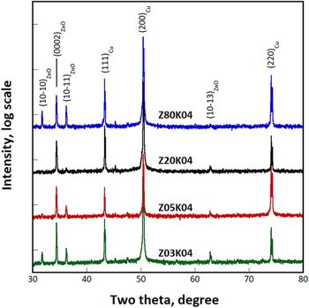
Figure 1. XRD patterns of samples deposited from electrolytes containing 0.0025 to 0.08 M zinc nitrate and 0.4 M potassium nitrate.
Download figure:
Standard image High-resolution imageSEM micrographs of the four samples are presented in Fig. 2. The low magnification micrographs in Figs. 2a, 2c, 2e and 2g show brightness variation from one Cu grain to another, indicating that the orientation of deposited ZnO crystallites was strongly influenced by the substrate grain orientation. The Z03K04 sample, deposited using the lowest zinc ion concentration, was composed of well-separated ZnO pillars (Fig. 2b). The hexagonal pillars were 50–200 nm in width and more than 1 μm in length. More than half of the pillars were aligned vertically to the substrate surface in the right and left areas, respectively. The hexagonal cap surfaces of the pillars appear to be aligned in the same direction. In the central area, four variants of pillar orientation existed. The dashed lines highlight the presumable grain/twin boundaries of the Cu grains. A similar phenomenon was observed for the Z05K04 sample, with the exception that the width of the pillars was slightly larger at 100–400 nm and the vertically aligned pillars had partly coalesced (Fig. 2d). The high-magnification micrographs of the Z20K04 and Z80K04 samples are displayed in Figs. 2f and 2h, respectively. The shape of the crystallites changed from pillar to plate and the width of the hexagonal cap surface increased to approximately 500 nm (Z20K04) and further to approximately 1000 nm (Z80K04) with an increase in the zinc ion concentration, although the total nitrate ion concentration changed only slightly. Moreover, each Cu grain was mostly covered by a single variant of ZnO crystallite, regardless of the (0001)ZnO basal plane orientation. For example, the four grains (labeled 1–4) visible in Fig. 2h were covered by ZnO plates with hexagonal caps oriented in the same direction. The angle between the hexagonal basal plane and substrate surface was estimated to vary from less than 5° to approximately 50°. Extensive ledges can be observed on the cap surfaces for the Z20K04 and Z80K04 samples, revealing that lateral growth along the 〈11 0〉 and/or 〈10
 0〉 directions was the dominant mechanism of crystal growth at high zinc ion concentrations.
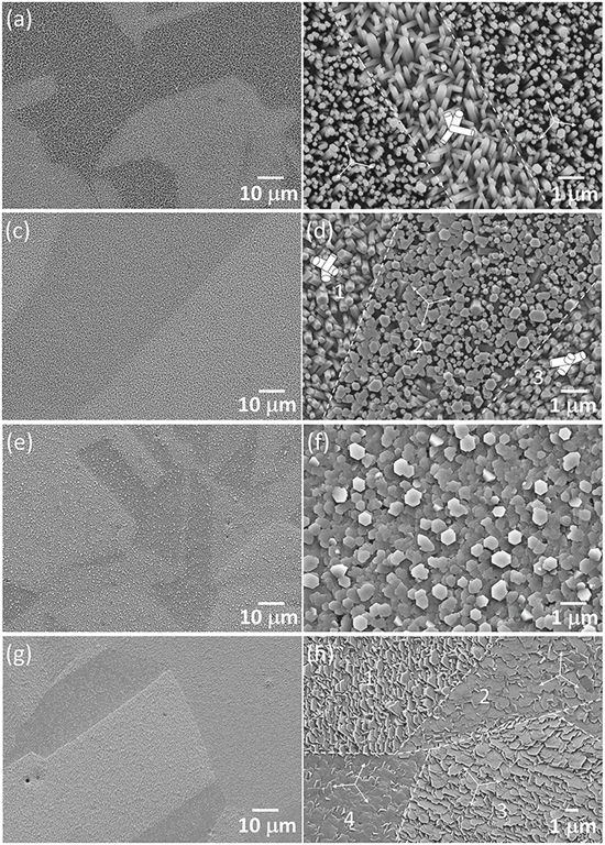
Figure 2. SEM micrographs of samples deposited from electrolytes containing (a), (b) 0.0025 M, (c), (d) 0.005 M, (e), (f) 0.02 M and (g), (h) 0.08 M zinc nitrate and 0.4 M potassium nitrate.
Download figure:
Standard image High-resolution imageThe results–ND and RD OIMs and the ND inverse pole figure (IPF)–of the EBSD analyses performed on the four samples were illustrated by a stereographic projection triangle for each sample in Fig. 3. Two distinct features were observed. First, the index rate of the OIM increased from 46% for Z03K04 (low zinc ion concentration) to 93% for Z80K04 (high zinc ion concentration). Typically, the index rate is affected by the size and orientation distribution of the crystallites and the flatness of the film. The finer the pillars, the lower the index rate. The local variation in the index rate from one grain to another reflects the condition of the epitaxial growth on grains of various orientations. A high index rate was obtained on a substrate grain covered by ZnO plates of mainly one orientation. This situation was most common for the Z80K04 sample on which the deposited crystallites exhibited the largest plate size and were stacked regularly (Fig. 2h). Therefore, the more zinc ions were added to the electrolyte, the more the crystallites grew epitaxially on the Cu substrate. Second, all the deposits exhibited a strong 〈0001〉//ND texture. The intensity of the ND//〈0001〉 pole increased from 8 (× random) to 18 with an increase in the zinc ion concentration from 0.0025 to 0.02 M. The maximum intensity of the Z80K04 IPF was, however, located at 〈10 5〉//ND instead of 〈0001〉//ND with a value of 9.5. The intensity of the 〈0001〉∼//ND texture, however, also varied among grains, demonstrating that the orientation of ZnO crystallites was strongly influenced by both the zinc ion concentration and orientation of Cu grains.
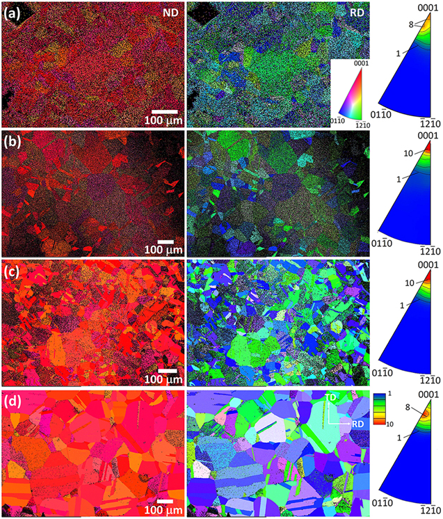
Figure 3. EBSD ND/RD OIMs and ND IPFs for the deposited ZnO films of the (a) Z03K04, (b) Z05K04, (c) Z20K04, and (d) Z80K04 samples.
Download figure:
Standard image High-resolution imageFigure 4 illustrates an ex situ EBSD analysis result for the Z03K04 sample. The analytical area corresponding to the OIM (Fig. 3a) was analyzed through EBSD prior to ZnO deposition. The substrate ND OIM is depicted in Fig. 4a, and the stereographic projection of Cu/ZnO of four grains (A-D) labeled in the OIM is illustrated in Figs. 4b–4e. Each stereographic projection was derived from the (100), (110), and (111) pole figures of Cu and the (11  0) one of ZnO, and the ZnO (0001) pole figure was overlaid. According to Fig. 4b, grain A has a 〈100〉//ND orientation and four ZnO variants (Z1–Z4) were present. Their 〈0001〉 poles surrounded a Cu 〈100〉 pole, and one of their 〈11
 0〉 poles was nearly parallel to the other 〈100〉Cu pole. Considering that the position of the sample on the stage after ZnO deposition could be twisted or inclined slightly with respect to how it was prior to the deposition, a deviation of 1°–5° was likely to exist between the orientations of Cu and ZnO. Accordingly, the orientation relationship between the ZnO variants and Cu, which was unexpected, could be described as follows: (0001)ZnO//(103)Cu and [11
 0]ZnO//[010]Cu, which is designated herein as V1. Four 〈103〉 Cu poles of the same group surrounded a 〈100〉 Cu pole, and twelve variants could be resulted. However, not only the orientation relationship but also the growth plane must be considered in epitaxial growth. The four variants surrounding one 〈100〉//ND pole had nearly equal opportunity to nucleate on the (100) plane. Figure 4c indicates that a major variant (Z1) and two minor variants (Z2 and Z3) of ZnO were present on a 〈110〉//ND grain following the same epitaxial orientation relationship. Z1 exhibited the smallest angle with respect to ND among the four variants of the same group. The high population of Z1 pillars could be attributed to the fast growth rate along the 〈0001〉 direction when deposition occurred from a low-zinc-ion-concentration electrolyte. The stereographic projection in Fig. 4d reveals that two ZnO variants were present on a 〈111〉//ND grain following V1, instead of the expected (0001)ZnO//(111)Cu, orientation relationship. Again, the variant with its 〈0001〉 pole closer to ND had higher intensity. Finally, Fig. 4e illustrates that the majority of the crystallites deposited on a 〈103〉//ND grain had a 〈0001〉//ND orientation. In addition to the major variant Z1, two more variants, Z2 and Z3, occupying approximately 20% of the crystallites, were observed. All three variants belonged to the same group of the V1 orientation relationship.
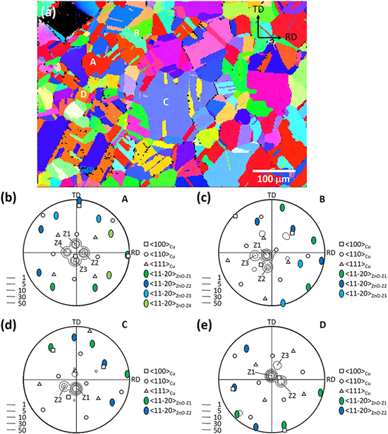
Figure 4. In-plane, ex situ EBSD analysis of the Z03K04 sample: (a) ND OIM of the substrate, and stereographic projections of (b) grain A, (c) grain B, (d) grain C, and (e) grain D showing the orientation of the substrate grain and overlaid ZnO.
Download figure:
Standard image High-resolution imageAccording to the OIMs of the Z80K04 sample (Fig. 3d), many Cu grains were overlaid by an epitaxial layer of a single orientation. To understand the orientation selection in the nucleation stage, the cross-section of the Z80K04 sample was analyzed using EBSD. The ND and RD OIMs of two positions, with each position containing two grains, are displayed in Figs. 5a and 5b, respectively. The thickness of the ZnO layer varied from one grain to another in a range of 380–580 nm, coinciding well with the theoretical value of 470 nm. The corresponding stereographic projection of Cu/ZnO of grain A, B, C1, and C2 are illustrated in Figs. 5c–5f, respectively. The OIMs shown in Figs. 5a and 5b indicate that grains A, C1, and C2 were overlaid with multiple variants of ZnO crystallites, whereas single-variant ZnO was deposited on grain B. The stereographic projection in Fig. 5c indicates that three variants of ZnO grew on the 〈111〉∼//ND grain (grain A) and all had the V1 orientation relationship. The area fraction of Z1 was approximately three times as high as that of Z2. Two small crystals of Z3, indicated by arrows in the ND OIM, can be observed. The crystallites grown on the 〈110〉//ND grain (grain B) exhibited mostly a single orientation and were very flat, as demonstrated in Figs. 5a and 5d. The orientation relationship between ZnO and Cu remained V1. Moreover, the stereographic projection in Fig. 5e indicates that the overlaid layer on a 〈100〉∼//ND grain (C1) was composed of four ZnO variants of the same group. Thus, their 〈0001〉 poles all surrounded the same 〈100〉 Cu pole. Crystallites of all variants nucleated with approximately equal opportunity, but only those of variant Z1 and Z2 grew preferentially. The ZnO layer deposited on grain C2 with a 〈100〉//ND orientation had uniform thickness (see Fig. 5b). Four variants of the same group are observed in the stereographic projection presented in Fig. 5f.
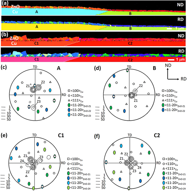
Figure 5. Cross-sectional EBSD analysis for the Z80K04 sample: (a), (b) ND/RD OIMs of two regions, and stereographic projections of (c) grain A, (d) grain B, (e) grain C1, and (f) grain C2 showing the orientation of the substrate grain and overlaid ZnO.
Download figure:
Standard image High-resolution imageThe room-temperature PL spectra of the samples deposited at various zinc nitrate concentrations are displayed in Fig. 6. Each spectrum displays two distinct features of near-bandgap emission (NBE) in the ultraviolet wavelength region and deep level emission (DLE) in the visible region (1.5–2.5 eV, or 500–800 nm) centered at 2.0–2.1 eV (590–620 nm). The peak at approximately 1.6 eV is a replica of the second order diffraction of the NBE peak. For each sample, the two spectra with the highest and lowest INBE /IDLE ratio are displayed. The NBE peaks are located within the energy range 3.25–3.29 eV, coinciding well with the reported value of 3.28 eV for the ZnO crystals. 21 The Z03K04 sample had low INBE/IDLE ratios of 0.3–2.1 with full width half maximums (FWHMs) of 124–230 meV. The spectrum of the Z05K04 sample, deposited from an electrolyte containing a higher zinc ion concentration, had the strongest NBE peak, highest INBE/IDLE ratios of 2.4–4.4, and lowest FWHMs of 122–131 meV among the four samples. With a further increase in the zinc ion concentration to 0.02–0.08 M, the intensity of the strongest NBE peaks halved. Because the INBE /IDLE ratio and the FWHM of the NBE peak were both strongly correlated with the defect density in the crystallites, the PL results reveal that the Z05K04 sample should had the lowest density of defects. 22
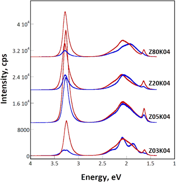
Figure 6. Selected PL spectra of four samples deposited from electrolytes containing 0.0025 to 0.02 M zinc nitrate and 0.4 M potassium nitrate at room temperature. (Red: highest INBE /IDLE ; blue: lowest INBE /IDLE ).
Download figure:
Standard image High-resolution imageEffect of KNO3 concentration on the morphology, epitaxial growth, and PL properties of ZnO films
Because the generation of hydroxyl ions relies directly on the concentration of nitrate ions, samples were deposited from electrolyte containing 0.1–2.0 M potassium nitrate and 0.02 M zinc nitrate to clarify the effect of nitrate ion concentration on the nucleation and growth of ZnO. Figure 7 shows the XRD patterns of five samples deposited with different potassium nitrate contents. The relative intensity of the (0002) reflection and the (10 0) reflection decreased gradually with an increase in the potassium nitrate concentration. At the highest KNO3 concentration of 2.0 M, the intensities of the (10
 1), (10
 2), and (10
 3) peaks were stronger than that of the (0002) peak. The aforementioned results revealed that the preferential growth direction of the crystallites was strongly affected by nitrate ion concentration.
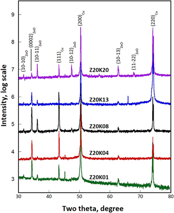
Figure 7. XRD patterns of samples deposited from electrolytes containing 0.2 M zinc nitrate and 0.1–2.0 M potassium nitrate.
Download figure:
Standard image High-resolution imageThe surface morphology is illustrated by the SEM micrographs presented in Fig. 8. The grain contrast in the low-magnification micrograph increased with an increase in the potassium nitrate concentration to 1.3 M, but this contrast was entirely absent in the micrograph of Z20K20 (Fig. 8g). The high-magnification micrograph displayed in Fig. 8b reveals that the crystallites were approximately 500 nm wide and thick. Multiple variants of crystallites were present in a Cu grain. The high-magnification micrographs shown in Figs. 8d and 8f clearly reveal that the crystal width increased to approximately 1000 nm and considerable coalescence among the crystallites had occurred when the KNO3 concentration was increased to 0.8 M and higher. Therefore, the samples deposited at 0.8 and 1.3 M exhibited lower roughness than their 0.1 and 0.4 M counterparts. At the potassium nitrate concentration of 2.0 M, only crystallites with basal plane inclined 30° or more with respect to the substrate surface were present, and multiple variants coexisted on one Cu grain (Fig. 8h). Each crystallite variant remained in a specific orientation relationship with the substrate.
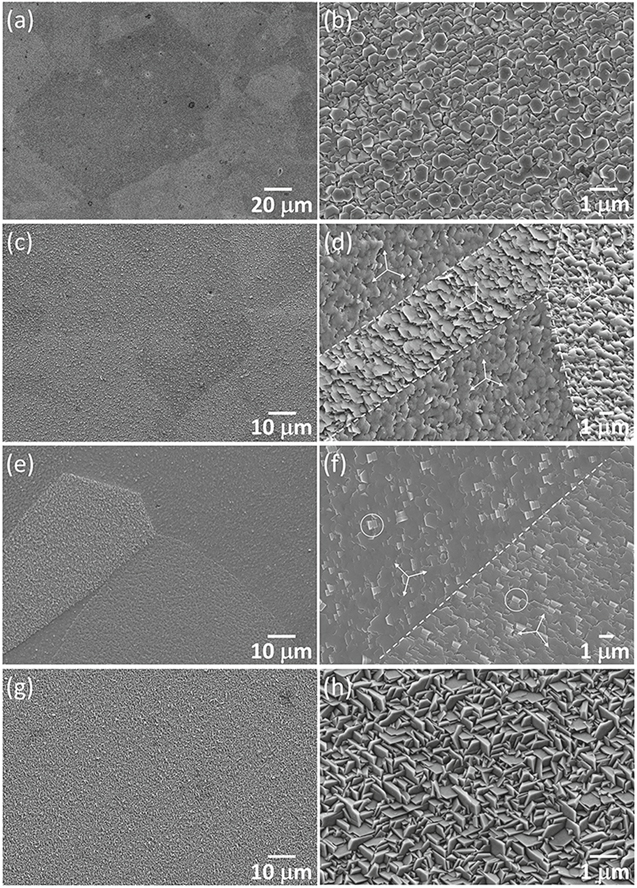
Figure 8. SEM micrographs of samples deposited from electrolytes containing 0.02 M zinc nitrate and (a), (b) 0.1 M, (c), (d) 0.8 M, (e), (f) 1.3 M and (g), (h) 2.0 M potassium nitrate.
Download figure:
Standard image High-resolution imageFigure 9 displays the ND/RD OIMs and ND IPFs of ZnO for the Z20K08, Z20K13, and Z20K20 samples. The OIMs of the Z20K08 and Z20K13 samples had high index rates of 68 and 75%, respectively, similar to that of the Z20K04 sample (67%). The Z20K08 sample had weak 〈10 1〉//ND texture in addition to strong 〈0001〉//ND texture. In addition, the Z20K08 sample exhibited moderate 〈10
 5〉//ND texture associated with strong 〈0001〉 texture. For the Z20K20 sample, the OIM had an index rate as low as 37% and a low maximum ND intensity of 3.4× random parallel to the poles of {10
 2} to {11
 3}. The low index rate resulted from interlocked crystallites of multiple variants.

Figure 9. EBSD ND/RD OIMs and ND IPFs of the (a) Z20K08, (b) Z20K13, and (c) Z20K20 samples.
Download figure:
Standard image High-resolution imageFigure 10 displays the EBSD results for the Z20K08 sample. The ND OIM of the substrate in Fig. 10a was acquired from a position the same as that in Fig. 9a. The ZnO deposited on grain A-D exhibited different orientation colors (Fig. 9a). For example, grains A and C were overlaid by a 〈0001〉//ND film consisting of a single variant of ZnO. By contrast, the ZnO crystallites deposited on grains B and D had at least two orientations. The stereographic projections shown in Figs. 10b and 10d verify the single-variant feature of the films grown on both grains. However, the ZnO deposited on grain A exhibited the V1 orientation relationship with Cu, whereas a new, but expected, orientation relationship was observed between ZnO and Cu for grain D: (0001)ZnO//(111)Cu and [10 0]ZnO//[1
 0]Cu, which is herein designated as V2. The multiple variant character of the ZnO grown on the 〈110〉//ND grain (grain B) is depicted in Fig. 10c. Variants Z1 and Z2 grew by following different epitaxial orientation relationships. The 〈0001〉 pole of Z1 was nearly parallel to a 〈001〉Cu pole, whereas that of Z2 was deviated by approximately 20° from one of the other 〈001〉Cu pole. Variant Z1 therefore exhibited a new epitaxial orientation relationship of (0001)ZnO//(100)Cu and [11
 0]ZnO//[001]Cu, which is herein designated as V3. The basal plane of Z1 crystallites were inclined at 50° from ND, which resulted in a rough surface (micrograph not shown). Figure 10e displays the stereographic projection of grain D, which had an orientation of 〈122〉∼//ND. At least four ZnO variants were present. Variant Z1 followed the V2 epitaxial orientation relationship; variant Z2, V3, and variants Z3 and Z4, the most popular V1. However, a close examination indicated that the 〈11
 0〉ZnO directions rather than 〈10
 0〉ZnO of Z1 were parallel to 〈110〉Cu, representing a 30° rotation of the V2 epitaxial orientation relationship. The epitaxial orientation relationship (0001)ZnO//(111)Cu and [11
 0]ZnO//[1
 0]Cu is herein designated as V4. Therefore, three more epitaxial orientation relationships were identified in this sample.
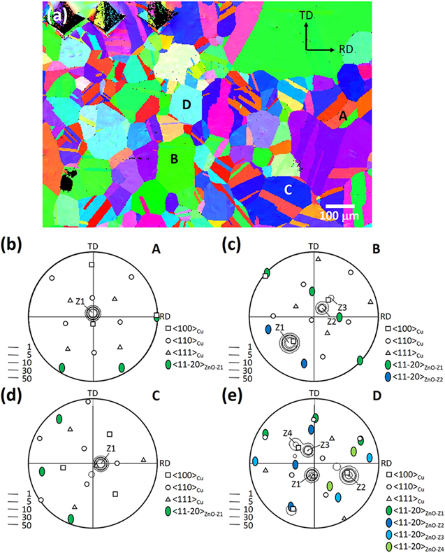
Figure 10. EBSD results for the Z20K08 sample: (a) ND OIM of the substrate, and stereographic projections of (b) grain A, (c) grain B, (d) grain C and (e) grain D showing the orientation of the substrate grain and overlaid ZnO.
Download figure:
Standard image High-resolution imageAs illustrated in Fig. 9, with an increase in the concentration of potassium nitrate to 1.3 M in the electrolyte, the orientation distribution of ZnO changed from its lower KNO3 concentration (0.8 M) counterpart. The ND OIM of the ZnO deposits shown in Fig. 9b exhibited strong 〈0001〉//ND texture, and the orientation contrast was smeared. The OIM of the Cu substrate of the same position is displayed in Fig. 11a, from which three grains were selected for orientation analyses. The stereographic projection of a 〈100〉//ND grain (grain A) is illustrated in Fig. 11b, indicating that a nearly 〈0001〉//ND epilayer was deposited with a V1 epitaxial orientation relationship. For a 〈110〉//ND grain (grain B), the stereographic projection (Fig. 11c) indicates that the deposits consisted of two ZnO variants possessing the same V1 epitaxial orientation relationship with respect to two 〈100〉 poles. Both the variants had the smallest angle with ND among those of the same group. The stereographic projection of a 〈111〉//ND grain (Fig. 11d) revealed that the ZnO variants followed the V1 rather than the V2 or V4 epitaxial orientation relationship. All the ZnO crystallites grown epitaxially in this sample follow the V1 orientation relationship.
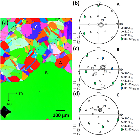
Figure 11. EBSD results for the Z20K13 sample: (a) ND OIM of the substrate, and stereographic projections of (b) grain A, (c) grain B, (d) grain C and (e) grain D illustrating the orientation of the substrate grain and overlaid ZnO.
Download figure:
Standard image High-resolution imageFigure 12 displays the PL spectra for the samples deposited at various potassium nitrate concentrations. Both the NBE intensity and INBE /IDLE ratio increase with an increase in the potassium nitrate concentration from 0.1 to 1.3 M. The Z20K13 sample containing ZnO films could generate luminescence with an INBE /IDLE ratio as high as 4.7. The NBE intensity decreased considerably when the concentration was further increased to 2.0 M, accompanied with a low INBE /IDLE ratio of 0.6–1.0. Accordingly, the samples on which ZnO crystallites of multiple variants were deposited had low NBE intensity and relatively high DLE intensity.
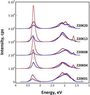
Figure 12. Selected PL spectra of four samples deposited from electrolytes containing 0.02 M zinc nitrate and 0.1–2.0 M potassium nitrate at room temperature. (Red: highest INBE /IDLE ; blue: lowest INBE /IDLE ).
Download figure:
Standard image High-resolution imageDiscussion
Crystallite morphology
The morphology of the ZnO crystals deposited in nitrate electrolyte is affected considerably by the zinc nitrate concentration. Nanopillars are obtained from electrolytes containing 0.01 M zinc nitrate or less. The width of the pillar increases, whereas the length decreases, with an increase in the zinc nitrate concentration. The crystallites change to a plate-like shape with a width-to-thickness ratio smaller than 1 at high zinc nitrate concentration.
5,8,10,12,13,15,23
However, it is unclear whether the preference for one-dimensional growth is controlled by the zinc or nitrate ion concentration. In this study, ZnO pillars were deposited from an electrolyte with a zinc ions concentration of lower than 0.02 M and total nitrate concentration of higher than 0.4 M. This result clearly demonstrates that the morphology is far more sensitive to zinc ion rather that nitrate ion concentration. Yoshida et al. proposed that the zinc ions function as a catalyst to mediate the charge transfer reaction and then react with the hydroxyl ions generated from the charge transfer reaction.
8
At a low zinc ion concentration, the transport of zinc ions to the electrode surface is the rate limiting step. Under the galvanostatic condition, a high overpotential has to be applied to drive the charge transfer reaction as soon as the zinc ions are absorbed on the outward (0001)ZnO plane. The crystals thus grow in a layer-by-layer mode on the (0001)ZnO plane. The rate limiting process changes to the interfacial reaction with an increase in the zinc ion content. Considering a polarization field along the 〈0001〉ZnO direction, nitrate ions are absorbed preferentially on the (0001)ZnO plane rather than the nonpolar {10 0}ZnO or {11
 0}ZnO planes. In this circumstance, more ledge sites on the (0001)ZnO plane and sites on the nonpolar sidewalls are available for zinc ions to absorb to, and the charge transfer reaction can proceed at a lower overpotential. The fast growth direction therefore changes from 〈0001〉 to 〈10
 0〉 or 〈11
 0〉. Figure 13 shows two high-magnification SEM micrographs for the pillars in the Z03K04 sample and plates in the Z80K04 sample. The cap surfaces of the pillars are flat and the pillars are slightly tapered with stepwise sidewalls (Fig. 13a), indicating that growth along the nonpolar directions was suppressed. However, ledges at high density are observed on the cap surfaces of the plates in the micrograph of the Z80K04 sample (Fig. 13b). The ledge and sidewall growth was dominant in this case. The hexagonal plates were therefore inversely tapered as indicated by the arrows in Fig. 13b. Figure 13c displays a schematic drawing of the growth modes at low and high zinc ion concentrations and the corresponding morphology.
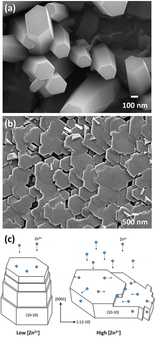
Figure 13. High magnificaction SEM mircographs of the (a) Z03K04 and (b) Z80K04 samples and (c) a schematic drawing illustrating the deposition mechanism at low and high zinc ion concentration, respectively.
Download figure:
Standard image High-resolution imageThe nitrate ion concentration weakly affects the morphology and growth mode of the ZnO crystallites. According to the SEM micrographs displayed in Fig. 8, the crystallites deposited from electrolyte containing 0.02 M Zn(NO3)2 and 0.1 M KNO3 had an average hexagonal cap surface width of 500 nm with a width-to-height ratio of approximately 1. The width of the cap surface increased to approximately 1000 nm as the KNO3 concentration was increased to 0.8 M; this was associated with a decrease of the width-to-height ratio to approximately 0.5. The width-to-height ratio was further decreased to approximately 0.3 as the KNO3 concentration was increased to 2.0 M. In addition to the preferential absorption of nitrate ions on the (0001) surface, which changes the growth mode, nitrate absorption is likely to decrease the surface energy of the (0001) plane relative to that of the nonpolar {10 0} planes.
24
The surface energy of (0001)ZnO was approximately three times as high as that of {10
0} planes.
24
The surface energy of (0001)ZnO was approximately three times as high as that of {10 0}ZnO, which was identified through SEM/EBSD of the sidewalls of the pillars and plates in the present case.
25
The equilibrium shape of the crystallites evolved from pillar to plate as a result of reduction of the surface energy of (0001)ZnO.
0}ZnO, which was identified through SEM/EBSD of the sidewalls of the pillars and plates in the present case.
25
The equilibrium shape of the crystallites evolved from pillar to plate as a result of reduction of the surface energy of (0001)ZnO.
Epitaxial growth and orientation relationships
Several scholars have demonstrated that ZnO, mainly in the form of rod, can be grown epitaxially on (111) Au, (111) Pt, and (0001) GaN substrates through electrodeposition. 16,18,26 However, substrates of other orientations or materials have not been used for the epitaxial growth of ZnO through electrodeposition. The epitaxial growth of ZnO on Cu substrate is dominated by nucleation of the crystallites. As mentioned, the charge transfer reaction prior to the deposition of ZnO occurred mainly through a catalytic effect provided by the zinc ions. Because the real thickness of the ZnO layer, as demonstrated in Fig. 6, was close to the theoretical thickness, almost all the hydroxyl ions generated in the charge transfer reaction were reacted with zinc ions to form ZnO when the zinc ion concentration in the electrolyte was high. The effective thickness of ZnO deposited from the electrolyte containing 0.0025 M Zn(NO3)2 was estimated to be approximately 250 nm, which was approximately half of the expected value. This low current efficiency was attributed to the nitrate ion reduction reaction [(reaction (1)] being catalyzed by copper. 27,28 Figure 14 displays the potential vs time curves of four samples. The deposition of ZnO from electrolyte with low zinc and nitrate ion concentrations should be performed at high overpotential. At a low zinc ion concentration, the overpotential was sufficiently high to allow the reaction to be conducted on exposed Cu surfaces. The hydroxyl ions generated in this case may not have reacted with the absorbed zinc ions, decreasing the current efficiency.
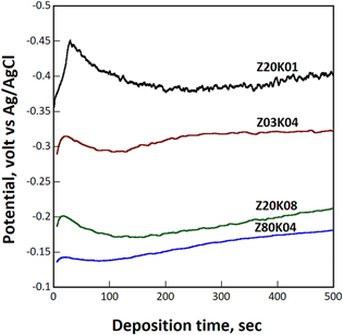
Figure 14. Linear sweep voltammetry curves of four samples in the initial stage of deposition.
Download figure:
Standard image High-resolution imageThe co-catalysis phenomenon could affect the epitaxial nucleation of ZnO crystallites on Cu substrates with various orientations. The reactivity of the nitrate reduction reaction is lower for (100)Cu than for (111)Cu and (110)Cu in an acidic environment.
29
The (111) or (110) surface can be covered by a layer of cuprous oxide, which promotes the absorption of nitrate ions.
30
In the present case, the nitrate reduction reaction catalyzed by zinc ions–that is, the nucleation of ZnO–was conducted rapidly on the (100)Cu surface or the ledges containing (100)Cu segments. Crystallites deposited following the V1 epitaxial orientation relationship could thus be understood, although it was unexpected because of the two-fold symmetry of the (103)Cu surface. Figure 15 displays atomic illustrations of ZnO and Cu, illustrating the (0001)ZnO//(111)Cu and (0001)ZnO//(103)Cu epitaxial orientation relationships. For the two possible atomic arrangements for the (0001)ZnO//(111)Cu epitaxy, the lattice mismatch along the [ 2
2 0]ZnO//[11
 ]Cu or [10
 0]ZnO//[1
 0]Cu direction was 9.3%, considerably smaller than that along the [
 2
2 0]ZnO//[1
 0]Cu direction using the lattice parameters obtained from XRD as aCu
= 0.3619 nm and aZnO
= 0.3257 nm. However, the lattice mismatches could be reduced to −1.4% and 1.2%, respectively, along the [
0]Cu direction using the lattice parameters obtained from XRD as aCu
= 0.3619 nm and aZnO
= 0.3257 nm. However, the lattice mismatches could be reduced to −1.4% and 1.2%, respectively, along the [ 010]ZnO//[30
 ]Cu and the [
 2
2 0]ZnO//[010]Cu directions if the coincidence site lattice (CSL) epitaxy was considered.
31
According to the analysis of lattice mismatch, the V1 epitaxial orientation relationship exhibited both low lattice mismatching and suitable strain accommodation. Thus, the tensile strain along [10
0]ZnO//[010]Cu directions if the coincidence site lattice (CSL) epitaxy was considered.
31
According to the analysis of lattice mismatch, the V1 epitaxial orientation relationship exhibited both low lattice mismatching and suitable strain accommodation. Thus, the tensile strain along [10 0]ZnO and the compressive one along [1
 10]ZnO could be relaxed by twisting the lattice slightly. The biaxial tensile strain accompanying the V3 orientation relationship was detrimental to epitaxial growth. The extremely high lattice mismatch of the V4 variant resulted in it being uncommon. However, the lattice mismatch of the V4 variant could be reduced to as low as 1.8% by introducing the CSL epitaxy (5×{220}Cu planes vs 4×{111
 0}ZnO planes). Figure 16 displays high-resolution TEM micrographs for the (0001)ZnO//(111)Cu and (0001)ZnO//(103)Cu cases, respectively. The interface for the former case (Fig. 16a) was slightly wavy in a range of 3 nm. The presence of the Moiré fringes at the interface indicated that it was not perfectly perpendicular to the paper surface but inclined slightly. The inverse Fourier transformed image in Fig. 16b reveals that dense interfacial dislocations were present at the interface in a way coinciding with the prediction of the CSL epitaxy. The dense interfacial dislocations were not preferable from an energy perspective. The seldom observed V2 and V4 orientation relationship s could thus be explained. The micrograph in Fig. 16c reveals that the interface was also wavy and not perfectly perpendicular to the paper surface when the sample was observed along the [
 2
2 0]ZnO//[010]Cu direction. Unlike the (0001)ZnO//(111)Cu case, the (0001)ZnO plane does not parallel to the interface which is presumable the (103)Cu plane. The angle between [0001]ZnO and [002]Cu was 16.0° according to the inverse Fourier transformed image in Fig. 16d, slightly smaller than the expect value of 18.4° derived from the V1 orientation relationship. The situation can be explained by the measured lattice constant of the a-axis of ZnO for the present sample being 0.3256 nm according to the XRD measurement, slightly higher than the theoretic value of 0.3250 nm. The lattice mismatch between four (
 010)ZnO planes and six 16° inclined (020)Cu planes was therefore as low as 0.1%. Accordingly, the TEM analysis revealed that the lattice mismatch played a crucial role in determining the epitaxial orientation relationship.
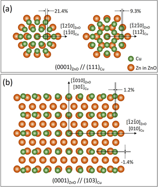
Figure 15. Schematic atomic strucutres of (a) the (0001)ZnO//(111)Cu epitaxial growth in two configurations and (b) the (0001)ZnO//(103)Cu epitaxial growth.
Download figure:
Standard image High-resolution image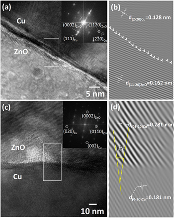
Figure 16. (a), (c) Cross-sectional TEM high-resolution images and (b), (d) inverse Fourier transformed image from the selected area for the ZnO films exhibiting (a), (b) a (0001)ZnO//(111)Cu, [11 0]ZnO//[1
 0]Cu and (c), (d) (0001)ZnO//(103)Cu, [11
 0]ZnO//[010]Cu epitaxial orientation relationship. Insets in (a) and (c) are the corresponding diffraction patterns obtained from Fourier transform.
Download figure:
Standard image High-resolution imagePhotoluminescence analyses
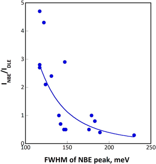
The PL results displayed in Figs. 6 and 12 are summarized in Table II. The NBE peaks were distributed at nominal energies of 3.27–3.29 eV with the FWHM ranging from 110–180 meV. Figure 17 illustrates the correlation of the FWHM of the NBE peak and the INBE /IDLE ratio for all the data displayed in Table II. Thus, the INBE /IDLE ratio increased with a decrease in the FWHM of the NBE peak. Both parameters were strongly affected by the defects present inside the crystallites and at the crystallite interfaces. Typically, the well-separated pillars should have been free from interface defects. However, the Z03K04 sample, deposited at a relatively high potential, contained numerous grown-in defects, leading to poorer PL characteristics compared with Z05K04. 10 The samples overlaid by plate-like crystallites (Z20K01 and Z20K20) presumably contained interfacial defects in high densities. However, the data in Table II indicate that some areas on the samples deposited from electrolytes allowing epitaxial growth of ZnO to proceed on Cu grains with proper orientations exhibited PL characteristics comparable with those of the Z05K04 sample, which contained pillars. Thus, high quality ZnO epilayers can be deposited electrochemically by using Cu substrates with appropriate orientation. It is worth mentioning that the trace metallic ions present in the electrolyte might be incorporated in the ZnO crystals and cause deep level emission in the visible region. However, the incorporation of the foreign ions in the deposits is a global phenomenon and should not correlate with the growth mode of the ZnO crystals. The variation of the INBE/IDLE ratio in each sample should not be responded to the doping effect. In addition, the INBE/IDLE ratio should be decreased with increasing the concentrations of zinc nitrate and potassium nitrate if the doping effect played a major role on the photoluminescence properties. Nevertheless, the data shown in Table II does not support this hypothesis.
Table II. PL results for samples deposited at different zinc nitrate and potassium nitrate concentrations.
| Sample | ENBE, eV | FWHM, meV | INBE/IDLE |
|---|---|---|---|
| Z03K04-1 | 3.28 | 230 | 0.3 |
| Z03K04-2 | 3.25 | 124 | 2.1 |
| Z05K04-1 | 3.27 | 131 | 2.4 |
| Z05K04-2 | 3.27 | 122 | 4.3 |
| Z20K04-1 | 3.28 | 140 | 1.0 |
| Z20K04-2 | 3.29 | 147 | 2.9 |
| Z80K04-1 | 3.29 | 148 | 0.5 |
| Z80K04-2 | 3.28 | 117 | 2.7 |
| Z20K01-1 | 3.32 | 189 | 0.4 |
| Z20K01-2 | 3.31 | 183 | 0.8 |
| Z20K08-1 | 3.28 | 146 | 0.5 |
| Z20K08-2 | 3.28 | 117 | 2.8 |
| Z20K13-1 | 3.29 | 142 | 0.7 |
| Z20K13-2 | 3.28 | 117 | 4.7 |
| Z20K20-1 | 3.27 | 176 | 0.5 |
| Z20K20-2 | 3.27 | 179 | 1.0 |
Figure 17. Correlation of the INBE /IDLE ratio and FWHM of the NBE peak with a line as a guide to the eye.
Download figure:
Standard image High-resolution image
Conclusions
A series of ZnO samples were electrodeposited on polycrystalline Cu substrates by adjusting the zinc nitrate and potassium nitrate concentrations in the electrolyte. The following conclusions can be drawn.
The morphology of the ZnO crystallites was mostly controlled by the zinc ion concentration of the electrolyte. Hexagonal pillars 50–400 nm in width were deposited at low zinc ion concentrations (<0.02 M), whereas plates of width 500–1000 nm were obtained at zinc ion concentrations of 0.02 M and higher. However, an increase in the nitrate ion concentration from 0.44 to 2.04 M resulted in a slight increase of the width-to-thickness ratio.
All the films had strong 〈0001〉//ND fiber texture. Most of the ZnO crystallites were grown epitaxially on Cu grains regardless of the electrolyte concentration. At a low nitrate ion concentration of approximately 0.4 M, only one epitaxial orientation relationship was identified, (0001)ZnO//(103)Cu and [11 0]ZnO//[010]Cu, regardless of the substrate grain orientation and zinc ion concentration. Three epitaxial orientation relationships were identified from the sample deposited from an electrolyte containing 0.8 M potassium nitrate and 0.02 M zinc nitrate: (0001)ZnO//(111)Cu and [10
 0]ZnO//[
 10]Cu, (0001)ZnO//(100)Cu and [11
 0]ZnO//[010]Cu, and (0001)ZnO//(111)Cu and [11
 0]ZnO//[
 10]Cu. TEM analyses revealed that CSL epitaxy was the main mechanism to accommodate large lattice mismatches between Cu and ZnO.
The overwhelming presence of the epitaxial orientation relationship of (0001)ZnO//(103)Cu and [11 0]ZnO//[010]Cu was attributed to the difference in the nitrate reduction activity of the (100) and (111) Cu surface.
The sample deposited from an electrolyte containing 0.4 M potassium nitrate and 0.005 M zinc nitrate, consisting of nanopillars, exhibited excellent PL characteristics with an INBE/IDLE ratio of 2.4–4.3 and FWHM of the NBE peak of 122–131 meV. The epitaxial layers resulted from coalesced plates formed from an electrolyte containing 1.3 M potassium nitrate and 0.02 M zinc nitrate also exhibited PL characteristics comparable with those of its nanopillar counterpart, indicating that the number of grown-in defects was effectively reduced.
Acknowledgments
We are grateful for the support provided by the Ministry of Science and Technology, R. O. C. under grant numbers MOST 107-2221-E-110-004-MY3 and MOST 108-2923-M-110-006-MY3, the support from the Center of Crystal Research at National Sun Yat-sen University, and the National Natural Science Foundation of China (U1605245).