

Abstract
Hydrogen gas (H2) is used as an alternative renewable and eco-friendly energy source to replace the fossil fuel. However due to its explosive risks in air, the H2 production, storage and transportation are greatly limited. Hence, H2 sensor with quick response, highly sensitive and selective detection is of importance. Recently, zinc oxide (ZnO) as n-type semiconductor has attracted much attention in the field of H2 detection because of its easy synthesis, chemical/thermal stability and extremely abundant nanostructures. The recent advances in resistive-type H2 gas sensors based on ZnO nanostructures are reviewed in this paper. According to zero-dimension, one-dimension, and two-dimension, the H2 sensing properties and related mechanism of various kinds of pristine ZnO nanostructures-based sensors, such as nanowires, nanotubes, and nanofibers are summarized and compared. Furthermore, this paper focuses on strategies to improve the performance of H2 sensors (sensitivity, response speed, operation temperature, and limit of detection) by the surface modification, metal doping, formation of composite, and post-treatment of ZnO nanomaterials. Especially, the selectivity of ZnO nanosturctures-based H2 sensors to H2 in the presence of interfering gases is highlighted and the related enhancement approaches are discussed. Finally, the outlook and challenges on the ZnO nanostructures-based H2 sensors are addressed as well.
Export citation and abstract BibTeX RIS

This is an open access article distributed under the terms of the Creative Commons Attribution 4.0 License (CC BY, http://creativecommons.org/licenses/by/4.0/), which permits unrestricted reuse of the work in any medium, provided the original work is properly cited.
Hydrogen gas (H2) has long been regarded as a clean and renewable energy carrier alternative to carbon-based fuels, which contributes to overcoming the global warming problem.1 It is widely used in industrial synthesis, petrochemical plant, biomedical application, nuclear power station and various energy fields, especially for fuel cell vehicles.2,3 However, due to its colorless, odorless, tasteless and explosion risks at concentrations range of 4–75 vol% in air, the H2 production, storage, transport, and usage are strictly limited. Therefore, it is imperative and necessary to develop a highly sensitive and selective H2 sensor with fast response to detect its concentration and prevent from its leakage.4,5 Table I lists the performance requirements of H2 sensors for different applicable fields.2 Normally, high sensitivity, short response/recovery time, wide range of detection and good environmental adaptability are needed.
Table I. Summary of requirements for H2 sensors in the different fields.2
| Field | Performance requirement |
|---|---|
| Stationary systems | Measuring range: up to 4 vol% H2 in air; Survivability at 100% |
| Detection limit <100 ppm | |
| Response time (t90) <30 s; Recovery time (t10) <60 s | |
| Ambient temperature: −20 to +50 °C; Ambient pressure: 80–110 kPa; Ambient humidity: 20%–80% relative humidity | |
| Accuracy: ±25% or 50% depending on H2 concentration | |
| Automotive systems | Measuring range: 0–4 vol% H2 in air; Survivability at 100% |
| Response time (t90) <3 s; Recovery time (t10) <3 s | |
| Ambient temperature: −40 to +125 °C; Ambient humidity: 0%–100% relative humidity | |
| Stationary power systems | Measuring range: up to 1 vol% H2 in air (alarm limit) |
| Lower detection limit <0.1 vol% | |
| Response time (t90) <30 s; Recovery time (t10) <30 s | |
| Durability/lifetime: 3–5 years; Calibration > lifetime | |
| Accuracy: 10% | |
| Automobile manufacturers | Measuring range: up to 4 vol% H2 min; Survivability at 100% |
| Detection limit <0.1 vol% | |
| Response time (t90) <1 s; Recovery time (t10) <1 s | |
| Ambient temperature: −40 to +85 °C; Ambient pressure: 62–107 kPa; Ambient humidity: 0%–95% relative humidity | |
| Power consumption <1 W; Lifetime: 6000 h | |
| Overall accuracy: ±5% of reading |
Many kinds of H2 sensors are developed to detect H2, such as acoustic wave, optical, thermoelectric, electrochemical, catalytic sensors and semiconductors metal oxide (SMO) sensor.1,5–8 SMO sensor is one of the most promising materials for gas sensing because of its simplicity in the design and fabrication, low-cost, good portability, and long-term stability.9–11 Among them, zinc oxide (ZnO) as n-type SMO has drawn great interest in the field of gas detection owing to its high electron mobility, easy synthesis, non-toxicity, chemical/thermal stability and extremely abundant nanostructures.12–14
In 1962, Seiyama et al.15 first discovered that the resistance of ZnO films changes with the adsorption and desorption of gas on its surface. Since then, ZnO has become a research hotspot of gas sensing materials. H2 sensors based on ZnO nanostructures have triggered an increasing attention around the world, such as ZnO nanowires (NWs),16,17 nanotubes (NTs),18,19 nanofibers (NFs),20,21 and thin films(TFs).22,23 Unfortunately, the pristine ZnO has poor sensing performance for H2 detection, for example, low sensitivity and selectivity, slow response/recovery time, and high operating temperature. Therefore, various methods and strategies have been utilized to improve the performance of ZnO-based H2 sensors such as noble metal modification, doping, nanocomposites (NCPs) and post-treatment. Although there are some related reviews on ZnO gas sensors or metal oxide H2 sensors, such as room-temperature gas sensing of ZnO-based gas sensor,24 gas sensors based on vertically oriented ZnO nanomaterials,25 metal oxide heterojunction gas sensor,26 metal oxide nanostructures for sensor applications,27 gas sensing mechanisms of metal oxide semiconductors,28 noble metal doped metal-oxide semiconductor for H2 sensor,29 gasochromic WO3 gas sensor-based hydrogen detection,30 resistive-type hydrogen gas sensor based on TiO2,31 and low-operating temperature resistive nanostructured hydrogen sensors including metal oxides, transition metal dichalcogenides, and graphene based nanomaterials,32 to the best of our knowledge, the comprehensive summary on resistive-type H2 sensors based on ZnO nanostructures is still rather lacking.
Therefore, in this work, recent advances on resistive type H2 sensors based on ZnO nanostructures are focused and reviewed. The sensing performance and related mechanism of various kinds of ZnO nanostructures for H2 detection are compared and summarized. Moreover, the strategy to improve the performance of H2 sensors based on ZnO nanomaterials is highlighted, especially for the H2 selectivity. Finally, the prospect and challenges for future ZnO-based H2 sensors are proposed.
ZnO Crystal Structure and Its Sensing Mechanism
ZnO is one of the most extensive and intensive researched materials because of their versatile electronic and optoelectronic properties. It is a wide direct bandgap semiconductor (3.37 eV) with a large exciton binding energy (60 meV). Compared to TiO2, the bulk ZnO and single nanowire ZnO exhibit much higher electronic mobility of 205–300 and 1000 cm2 V s−1, respectively.33 Moreover, ZnO is an environmentally friendly, chemically and thermally stable, and low-cost material, which is widely used in numerous fields, such as field-effect transistors, piezoelectric and varistor devices, solar cells, photocatalysis, UV detectors, light-emitting diodes, acoustic wave devices, biosensors, and gas sensors.25,27,33–35
ZnO has three kinds of crystal structures of hexagonal wurtzite, cubic zinc blende, and NaCl-type rock salt. Among them, hexagonal wurtzite is the most stable and common crystal structure of ZnO in ambient conditions, which is suitable for resistive-type gas sensing application. It is tetrahedrally coordinated with Zn and O atoms stacked alternatively along the c-axis, containing various face terminations—polar Zn-terminated (0001) and O-terminated (0001) facets, and non-polar mix terminated (1010) facets with an equal number of Zn and O atoms.36 The polar (0001) crystal facets have high surface energy and crystal growth rate than non-polar facets, leading to an anisotropic growth. By tuning the growth conditions, extremely abundant ZnO nanostructures, such as nanospheres,37 nanorods (NRs),35 NWs,38 NTs,39 nanosheets,40 nanoflake,41 nanoclips,13 and nanoflowers,42 have been fabricated successfully by a series of techniques of hydrothermal method, sol-gel process, electrospinning method, electrochemical deposition, vapor-phase transport process, metal-organic chemical vapor deposition (MOCVD), thermal evaporation, RF sputtering, pulsed laser deposition, solution-based polyol process, etc.13,27,43–45
The resistive gas sensor is one of the recognized sensor work principle by measuring the sensor resistance changes while introducing the target gas. The study on sensing mechanism of ZnO-based H2 gas sensor is essential and useful for the fabrication of outstanding H2 sensor. In a resistive-type gas sensor, n-type semiconductor ZnO sensing material is deposited on two or more electrodes by various methods. Upon exposure or withdrawal to H2 gas on the surface of ZnO, the changes in resistance of the sensor are measured during the adsorption and desorption of H2 gas, as shown in Fig. 1a. At first, oxygen molecules in air with higher electron affinity (0.43 eV) are easily adsorbed on the surface of ZnO according to the following reactions.21,46,47


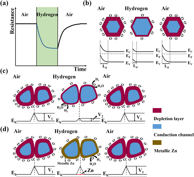
Figure 1. (a) Schematic of resistance change of ZnO during H2 detection; (b) Surface charge layer model; (c) Grain boundary barrier model; (d) Valence control model.
Download figure:
Standard image High-resolution imageThe adsorbed oxygen can extract electrons from the conduction band of ZnO and becomes the surface oxygen ions, leading to the decrease of the carrier concentration in ZnO with increased resistance. At different operating temperatures, different charged oxygen ions are formed. While H2 gas is introduced into the environment, H2 molecules can easily interact with adsorbed oxygen ions on the surface of ZnO. And the released electrons go back to the conduction band of ZnO, causing a drop in electrical resistance of ZnO, as described by the following equation.20,48

The gas sensing mechanism of ZnO can be described simply by the following three models along with the actual situations: surface charge layer model,17,18,47,49 grain boundary barrier model,20,47,50,51 and valence control model.17,48,52–54
Surface charge layer model
Normally, the conductivity of material is affected by the thickness of depletion layer. After the ZnO nanoparticles (NPs) are exposed to the air, low charge density will exist near the surface and the conductive channel becomes narrow, which leads to the resistance increasing. The region with low electron density nearby the surface is defined as the electron depletion layer (EDL), whose depth is called as Debye length (LD), as shown in Fig. 1b. The LD is typically on the order of ∼20–22 nm for ZnO at 250 °C–300 °C based on the following formula,45,55

where εo is the static dielectric constant, kB is the Boltzmann constant, T is the absolute temperature (523 or 573 K), q is the electrical charge of the carrier, and Nc is the carrier concentration of ZnO (5.1 × 1016 cm−3), and k is relative permittivity of wurtzite structure ZnO (7.8).
When exposed to a reducing gas of H2, the depletion layer thickness is reduced, causing a measurable change in the electrical conductivity of the material. For single crystal ZnO nanostructures, the conductivity of the material is affected mainly by the thickness of EDL, and generally the increase of EDL thickness generates better H2 sensing performance.17,18,47,49
Grain boundary barrier model
When ZnO materials are polycrystalline structures with a large number of grain boundaries, the movement of electrons has to go through the grain boundaries. In grain boundary barrier model, the sensor resistance is mainly determined by contact resistance between the crystal grains. As described above, oxygen molecules adsorbed on the surface of ZnO capture electrons from the ZnO conduction band in air and a higher barrier height between the ZnO grains will form. When exposed to H2 gas atmosphere, the decreased barrier height causes a resistance decrease of ZnO for H2 monitoring (Fig. 1c).20,47,50,51
Valence control model
While the reducing gas is adsorbed on the ZnO surfaces, valence state of Zn ions and ZnO energy band are altered based on valence control model, as indicated in Fig. 1d. At higher operating temperature, ZnO can be strongly reduced to Zn metal by a strong reducing agent of H2, which will produce a significant drop in the resistance of sensing ZnO and contribute to a higher sensitivity.17,48,52–54 The H2-induced metallization effect of ZnO will play a crucial role in improving the sensitivity and selectivity of ZnO-based H2 sensors in the following part.
H2 Sensing Properties of Pristine ZnO Nanostructures-Based Sensors
The H2 sensing performance of pristine ZnO materials can be tuned by reducing the size into nanometer level and designing the particular structure/morphology. Some work has confirmed that the gas sensing activity of hexagonal wurtzite ZnO is related to crystal facets.43,56 Owing to the unsaturated oxygen coordination, the Zn terminated (0001) planes more easily adsorb the oxygen species than the O-terminated (0001) and non-polar (1010) facets, showing a robust chemisorption process. In consequence, the gas sensing activity of the ZnO crystal facets in reducing target gas decreases in the order of (0001) > {1010} > {1011} and (0001).56 In addition, ZnO nanomaterials probably have larger specific surface area and lots of nanograins with more grain boundaries and higher barrier height between the grains, which increases the adsorption of H2 molecules and oxygen species on the surfaces with the improved sensitivity of H2 sensor. In the recent years, there are many researches on ZnO nanostructures, such as NPs, NWs, NTs, NFs, and nanobelts for H2 sensing. According to zero-dimension (0D), one-dimension (1D), and two-dimension (2D), the H2 sensing properties of different pristine ZnO nanostructures-based sensors without any modification are summarized in Table II.
Table II. Summary of H2 sensing properties of pristine ZnO nanostructures-based sensors.
| Dimension | Morphology | T (°C) | Conc. (ppm) | Resp. | tres/trev | LoD (ppm) (Resp.) | References |
|---|---|---|---|---|---|---|---|
| Zero-dimension | NPs (d = 45 nm) | 80 | 1000 | 48a) | — | 10(17a)) | 57 |
| NPs (d < 25 nm) | 200 | 50 | 18a) | <20 s/>200 s | 1(—) | 49 | |
| Nanospheres (d ∼ 200 nm) | RT | 20000 | 0c) | — | — | 37 | |
| RT/UV | 20000 | 39%c) | ∼10 s/∼10 s | — | 37 | ||
| One-dimension | NWs (D ∼ 25 nm) | 150 | 1000 | 43a) | 54 s/5 s | — | 58 |
| Single NW (D = 100 nm) | RT | 100 | 34%b) | 64 s/11 s | 100 | 55 | |
| NWs (D = 100 nm) | 300 | 100 | 2.63a) | — | 1(2.3a)) | 17 | |
| NWs (D ∼ 30–80 nm) | 200 | 2000 | 2.93a) | ∼160 s/180 s | — | 16 | |
| Single NW (D ∼ 100–150 nm) | 200 | 100 | 2.5a) | ∼30 s/∼290 s | 50(∼1.8a)) | 59 | |
| Multiple NWs | 200 | 100 | 5.3a) | ∼30 s/∼310 s | 50(2.5a)) | 59 | |
| Single NW (D = 200 nm) | RT | 4500 | ∼90%d) | 55 s/100 s | 500(∼55%d)) | 60 | |
| NTs (t ∼ 42.7 nm) | 250 | 1000 | 139.11a) | 80 s/260 s | 10(7.31a)) | 39 | |
| NTs (t ∼ 42.7 nm) | 250 | 100 | 10.69a) | ∼106 s/250 s | — | 39 | |
| Porous NTs (t ∼ 30 nm) | 200 | 5000 | 7.57a) | ∼50 s/∼180 s | 100(1.48a)) | 18 | |
| NTs (t ∼ 30 nm) | 200 | 5000 | 3.03a) | >200 s/>200 s | 100(1.21a)) | 18 | |
| NTs (t ∼ 80 nm) | RT | 500 | 29.6%b) | ∼8 min/∼8 min | 5(11.9%b)) | 61 | |
| NTs (D ∼ 80 nm) | 200 | 1000 | 18a) | longer | — | 58 | |
| Aligned NTs (D ∼ 200 nm,d ∼ 17.8 nm) | 300 | 100 | 2.51a) | 17 min/3 min | — | 62 | |
| NRs (D ∼ 42 nm) | 300 | 3000 | 36.5%c) | 120 s/80 s | 1000(∼22%c)) | 63 | |
| NRs (D ∼ 35 nm) | 200 | 1000 | 32a) | 52 s/<10 s | — | 58 | |
| NRs (D ∼ 180 nm) | 250 | 50 | 2.15a) | — | 5(∼1.17a)) | 64 | |
| Aligned NRs (D ∼ 10–30 nm) | 350 | 2500 | 25a) | <10 s/<20 s | 10(∼3.8a)) | 65 | |
| NFs (D ∼ 100 nm, d ∼ 30 nm) | 350 | 10 | 109.1a) | ∼100 s/∼250 s | 0.1(∼22a)) | 66 | |
| Two-dimension | TFs(d ∼ 43 nm, t ∼ 10 nm) | 300 | 200 | 2a) | ∼450 s/500 s | 200 | 67 |
| TFs(d ∼ 21 nm, t ∼ 260 nm) | 350 | 200 | 98%b) | ∼380 s/200 s | 50(78%b)) | 68 | |
| Porous TFs (t ∼ 30 nm) | 200 | 5000 | 1.85a) | <200 s/<200 s | 100(1.13a)) | 18 | |
| TFs (d ∼ 15.5 nm, t) | 300 | 100 | 1.93a) | — | — | 62 | |
| Nanobelts (t ∼ 10 nm, W ∼ 40 nm) | 385 | 10000 | 14.3c) | 48 s/336 s | 600 | 44 |
Notes: NP, NW, NF, NR and TF denotes nanoparticle, nanowire, nanofiber, nanorod, and thin film, respectively. d refers to the grain size in NPs, TFs or NFs. t refers to the thickness of TF, NTs wall or shell. a)S = Ra/Rg = Ig/Ia. b)S = (Ra-Rg)/Ra. c) S = (Ig-Ia)/Ia = (Ra-Rg)/Rg = (Ga-Gg)/Ga. d)S = (Ig-IAr)/IAr; Ig, Ia and IAr is the current in the H2 gas, air and argon gas, respectively; G denotes conductance. — refers not available. RT denotes room temperature. T, Conc. and Resp. denotes temperature, concentration and response, respectively. tres and trev denotes the response and recovery time, respectively. LoD refers limit of detection.
By careful comparing pure ZnO nanostructures-based sensors' results from various dimensions, especially under similar conditions, it is found that in general 1D ZnO nanostructures such as NWs, NTs and NFs exhibit better H2 sensing performance than 2D ones of TFs and nanobelts and 0D ones of NPs and nanospheres, for example relatively higher sensitivity and slight lower work temperature.
First, the H2 sensing activity of single ZnO NW-based sensor at room temperature (RT) is introduced.60 ZnO NW (diameter of 200 nm) is MOCVD-derived single crystalline without noticeable defects, as seen in Fig. 2a. Pt/ZnO single NW Schottky diodes fabricated by e-beam lithography exhibit good H2 sensing properties of 1.9a with a faster response time of 55 s at RT in Fig. 2b. This is attributed to low barrier height of 0.42 V in ZnO/Pt Schottky junction and higher surface-to-volume ratio of ZnO NW surface at RT. Single ZnO NWs allow quick diffusion of H2 gas into and out the nanostructure. Thus, the rapid reaction rate leads to a higher sensitivity with faster response and recovery.60 In addition, multiple ZnO NWs devices are more sensitive than single ZnO NW devices due to the nanojuction effect in the multiple NWs ones as potential barrier for electron flow, however it also cause a significant diffusion resistance in the recovery period because of the lower O2 diffusivity.59
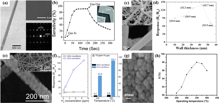
Figure 2. (a) Bright field Transmission Electron Microscope (TEM) images of ZnO NWs grown on c-plane sapphire. The inset shows the corresponding HRTEM (top) and SAED (bottom) pattern; (b) Room-temperature response behavior for 2500 ppm of H2; The inset shows the Scanning Electron Microscope (SEM) image of a representative Pt/ZnO NW Schottky diode.60 (c) Low magnification SEM image of porous ZnO NTs (top) and enlarged image (bottom); (d) Electrical response graph based on wall thickness of ZnO NT sensors during supply of 1000 ppm H2 at 250 °C.39 (e) FE-SEM images taken from ZnO NFs; The inset presents corresponding low-magnification image; (f) sensor responses of ZnO and SnO2 NFs for various H2 concentrations at 350 °C and sensor responses of ZnO and SnO2 NFs at 10 ppm H2 at 300 and 350 °C.66 (g) FESEM image of ZnO TFs on SiO2/Si substrate; (h) Sensitivity of the ZnO TFs for 200 ppm of H2 gas at different operating temperatures.68
Download figure:
Standard image High-resolution imageFor ZnO NWs or NRs gas sensors, the diameter (D) of NWs or NRs has a significant impact on H2 sensing performance. According to the theory of Rothschild et al.,69 when D is comparable to 2LD, the NWs or NRs sensors' response will tend to maximum value. From Table II, it can be observed that with decreasing the D of ZnO NWs or NRs from 100–200 nm to several tens of nanometers, the H2 sensing response becomes larger on the whole.57,58,65
Hollow 1D NTs sensor also shows similar tendency, as illustrated in Figs. 2c and 2d. When the wall thickness (t) of ZnO NTs is around 42.7 nm, equal to 2LD at 250 °C, the highest sensitivity of 139.1a is achieved.39 Moreover, compared to NWs and NRs, the oxygen species can be adsorbed both inner and outer sides of NTs,70 producing stronger response to H2. However, NTs' hollow structure with high aspect ratio will also affect the gas diffusivity, leading to longer diffusion time, especially for recovery time.18,39 Porous ZnO NTs sensor presents 2.5 times and 4.2 times improvement in the H2 sensing activity than nonporous ZnO NTs and porous ZnO thin films sensors, respectively.18
Similarly, the performance of H2 sensor based on ZnO can be effectively tuned by controlling the grain size (d). When d ≤ 2LD, the whole nanoparticle experiences electron depletion; When d > 2LD, EDL only appears at the surface region.45 In the former case, the resistance, i.e. the H2 response, strongly depends on the grain size. The smaller grain size is beneficial for the sensitivity of gas sensors, but excessive drop in d reduces structural stability, producing a deleterious effect on the temporal stability of the sensors.11 In the latter case, the resistance is limited by the Schottky barrier at grain boundaries in independent of the grain size.
Recently, the outstanding H2 sensing performance of ZnO NFs-based sensors has been reported in much literature.20,21,47,48,51 Nanofibers contain numerous nanograins with porous structure and higher specific surface area, so large amounts of H2 can easily diffuse along the grain boundaries, resulting in the improved H2 sensing performance. Figure 2e records pristine ZnO NFs' morphologies with d of ∼30 nm and Fig. 2f displays the sensor responses of ZnO and SnO2 NFs at various H2 concentrations and work temperatures.66 It is easily observed that ZnO NFs exhibit excellent H2 response of 139a at 250 °C to 1000 ppm H2 and better selectivity (see Fig. 6b) than SnO2 NFs. It is ascribed to the semiconductor-to-metal transition from ZnO to Zn at the surface of nanograins induced by H2 gas molecules, leading to more effective resistance modulation to ZnO NFs with the exceptional response and selectivity, in comparison with SnO2 NFs.66
Finally, we also show the morphology and H2 sensitivity of the ZnO TFs by RF sputtering in Figs. 2g and 2h.68 The ZnO TFs has strong (002) c-axis orientation with average d of 20.8 nm, very close to LD, which displays better response of 50a at 350 °C to 200 ppm H2. However, by and large, pristine ZnO TFs sensors have worse gas sensitivity owing to smaller specific surface area.18,62,67
Strategy to Improve H2 Sensing Performance of ZnO Nanostructures-Based Sensors
The ZnO nanostructures can be used as sensing layer for H2 gas sensor. Although pure ZnO NFs-based sensors exhibit admirable H2 sensing characteristics at higher operation temperature of 350 °C66 and single ZnO NW-based nanoscale sensors presents better H2 sensing activity at RT,55,60 in most cases, pristine ZnO still has some demerits such as higher operation temperature, worse selectivity, longer response time/recovery time, and relatively lower sensitivity in the H2 sensing. Hence, great attention has been paid to improve the sensing performance of ZnO based H2 sensors. Quite a few approaches have been taken to improve the H2 sensing properties of ZnO, as summarized in Table III. Several kinds of effective strategies, such as surface modification, doping, composite and post-treatment, are elaborated as follows.
Table III. Summary of H2 sensing properties of ZnO-based H2 sensors by various improvement strategies.
| Strategy | Classification | System | T (°C) | Conc. (ppm) | Resp. | tres/trev | LoD (ppm) (Resp.) | References |
|---|---|---|---|---|---|---|---|---|
| Modification | Noble metal | Amorphous-Pd/ZnO NRs | RT | 20000 | 12400%c) | 227 s/95 s | 100(50%c)) | 71 |
| Pd/ZnO NWs | 350 | 100 | 87.17a) | — | 0.1(∼8a)) | 17 | ||
| Pd/ZnO NWs | RT | 100 | 13100a) | 6.4 s/7.4 s | 100 | 72 | ||
| Pd/ZnO NWs | 200 | 10 | 4.3a) | — | 10 | 54 | ||
| Pd/ZnO NFs | 350 | 0.1 | 45.6a) | ∼300 s/∼40 s | 0.1 | 48 | ||
| Pt NPs@ZnO films | 300 | 75 | 80%b) | ∼10 min/∼25 min | 75 | 73 | ||
| Pt/ZnO NRs | RT | 1000 | 2.92a) | 47 s/48 s | 250(∼2.2a)) | 74 | ||
| Au-NPs/ZnO-NWs | RT | 100 | 7.5a) | 180 s/320 s | 20(2.25a)) | 75 | ||
| Networked Au/ZnO NWs | RT | 100 | 40a) | 140 s/300 s | 30(4.9a)) | 76 | ||
| Pt/ZnO NRs | 130 | 250 | 3.5a) | 27 s/— | — | 77 | ||
| Au/ZnO NRs | 130 | 250 | 16.3a) | 21 s/— | — | 78 | ||
| (Pt+Au) NPs/ZnO NRs | 130 | 250 | 59.1a) | 19 s/— | — | 78 | ||
| Pt-Au alloys NPs/ZnO NRs | 130 | 250 | 157.4a) | 15 s/— | 50(∼15a)) | 78 | ||
| RT | 250 | 25a) | — | — | 78 | |||
| Pt/Pd C-S NPs/ZnO NRs | 100 | 10000 | 58%b) | 5 s/76 s | 0.2(25%b)) | 79 | ||
| Pd/In2O3-Loaded ZnO NFs | 350 | 5 | 220a) | — | 0.05(∼152a)) | 80 | ||
| Metal oxide | WO3 NPs/ZnO NWs | 200 | 2000 | 12.6a) | ∼90 s/∼90 s | 100(∼2.1a)) | 16 | |
| PdO NPs/ZnO NRs | 450 | 1000 | 8.23a) | 153 s/68 s | 100(—) | 81 | ||
| Carbon | C NFs/ZnO TFs | 150 | 100 | 73.5%b) | 40 s/326 s | — | 82 | |
| rGO/Ni doped ZnO TFs | 150 | 100 | 63.8%b) | 28 s/210 s | 1(—) | 72 | ||
| Doping | Metal doping | Al doped ZnO TFs | 300 | 1000 | 66%b) | ∼320 s/440 s | 100(15%b)) | 23 |
| Mg doped ZnO TFs | 300 | 5 | 15a) | ∼500 s/∼500 s | 5 | 67 | ||
| Cd doped ZnO NRs | 220 | 1000 | 6.13e) | ∼50 s/30 s | 100(2.7e)) | 83 | ||
| Co doped ZnO NRs | 300 | 3000 | 99.2%c) | 74 s/40 s | 1000(55.6%c)) | 63 | ||
| Ni doped ZnO nanoplates | 150 | 10000 | 69%b) | — | 1(10%b)) | 84 | ||
| In doped ZnO TFs | 350 | 5 | 15%b) | — | 1(5%b)) | 85 | ||
| Cu-doped ZnO TFs | 150 | 1000 | 51%b) | 65 s/250 s | 10(2%b)) | 86 | ||
| Ga-doped ZnO TFs | 330 | 2500 | 4.23c) | ∼20 s/>800 s | — | 50 | ||
| Composite | Nano-Composite (NCP) | ZnO-SnO2 composite NFs | 350 | 0.1 | 78a) | 74 s/289 s | 0.03(3.6a)) | 51 |
| Graphene/ZnO NCP | 150 | 200 | 3.5a) | 22 s/90 s | 10(∼1.1a)) | 87 | ||
| rGO/ZnO NCP thick films | 250 | 500 | 30%c) | — | — | 88 | ||
| SnO2-ZnO composite NFs | 300 | 0.05 | 50.1a) | — | 0.02(∼3a)) | 20 | ||
| NiO-ZnO composite NFs | 200 | 10 | 60%b) | ∼50 s/∼90 s | 0.1(12.5%b)) | 21 | ||
| 50 | 10 | 38%b) | — | 5(∼3%b)) | ||||
| Co3O4-ZnO composite NFs | 300 | 10 | 133.65c) | ∼75 s/∼75 s | 1(50c)) | 89 | ||
| In2O3-ZnO composite NFs | 350 | 5 | 114a) | — | 0.05(72a)) | 80 | ||
| Core–shell (C-S) | ZnO@ZIF-8 C-S NRs | 250 | 50 | 3.28a) | ∼700 s/∼800 s | 5(1.33a)) | 64 | |
| ZIF-8/Pd/ZnO NWs | 200 | 50 | 8.5a) | — | — | 54 | ||
| ZnO-In2O3 C-S NRs | RT | 5 | 7.4%b) | ∼8 min/∼8 min | 5 | 90 | ||
| ZnO-SnO2 C-S NWs | 250 | 200 | 89%b) | — | — | 91 | ||
| Nb2O5-ZnO C-S NRs | 300 | 10000 | 568.3a) | — | — | 92 | ||
| Post-treatment | UV irradiation | Au/rGO/ZnO NCP | RT | 500 | 96%b) | 8 s/612 s | 30(44.6%b)) | 93 |
| UV irradiation | Au NP/ZnO TFs | 250 | 1000 | 1.72c) | 4 s/68 s | 50(0.79c)) | 94 | |
| EB irradiation | ZnO NFs | 350 | 10 | 150a) | — | 0.1(31a)) | 47 | |
| γ-irradiation | Vertically aligned ZnO NRs | 150 | 10000 | 77%b) | 19 s/147 s | — | 95 | |
| 500 °C PA in O2 | ZnO TFs | 400 | 120 | 1200a) | 90 s/— | 40(30a)) | 96 | |
| 400 °C PA in air | ZnO TFs | 100 | 500 | 140c) | — | 100(∼12c)) | 97 |
Notes: e)S = RN/Rg; RN is the initial resistance value of sensor in N2. NCP denotes nanocomposite; EB refers electron beam. PA refers to post-annealing. The other symbols are the same as in Table II.
Surface modification
In this section, the effect of surface modification of ZnO on the performance of H2 sensors is discussed. Herein the surface modification main relates to the noble metals, metal oxides and carbon materials. Among them, the incorporation of noble metal NPs on ZnO nanostructures is the most common and valid method for ameliorating the performance of H2 gas sensor.
The most commonly used noble metals are Pd, Pt and Au,29,98 which have higher catalytic activity in gas sensing application. Compared to unsensitized pristine ZnO, these noble metals NPs loaded on ZnO surfaces can reduce the adsorption energy of gases, which facilitates the adsorption of more oxygen species and H2 molecules on the ZnO surface with more surface active sites as a result of the well-known spillover effect (Figs. 3a and 3b).24 Simultaneously, noble metals have higher work function than ZnO, thus the electrons will migrate from ZnO conduction band to metal when in contact with ZnO, which creates the additional surface depletion layer than pristine ZnO, as indicated in Fig. 3c.24 Furthermore, Schottky barrier formation at the interfaces of metal and ZnO can effectively prevent from the recombination of electron-hole pairs.73,75,99

Figure 3. (a) Schematic diagrams presenting depletion layer of unsensitized ZnO. Schematic illustration of (b) chemical effect (spill-over phenomenon) and (c) electric effect of noble metal sensitized ZnO.24 (d) Energy band diagram showing the effect of the work function on the depletion region and hence the response of the M/ZnO sensor (M: Ag, Au, Pt); (e) Comparison of the response of different sensors (ZnO, Ag/ZnO, Au/ZnO, Pt/ZnO) to (300, 600, 1200) ppm of H2 @ 400 °C and insert shows the FESEM micrographs of heat-treated PtNPs@ZnO TFs.73 Response curves of the bare (f) and Pd-functionalized (g) ZnO NW sensor exposed to 1, 10, and 100 ppm of C6H6, C7H8, and H2 gases at 350 °C; The inserts show FE-SEM micrographs of the (f) bare ZnO NW and (g) Pd-functionalized ZnO NW.17 (h) The HRTEM images of the ZnO NRs supported Pt-Au NPs, inset is the EDS spectrum. (i) Sensing response of Au/ZnO, Pt/ZnO, (Pt+Au)/ZnO, PtAu/ZnO to different concentration of H2.78
Download figure:
Standard image High-resolution imageDrmosh et al. investigated the effect of Pt, Au and Ag NPs on energy band and H2 gas response of 40 nm-thick (002)-oriented ZnO TFs, as illustrated in Figs. 3d and 3e.73 It is found that Pt NPs@ZnO with larger work function of 5.6 eV results in an increased depletion layer and an evident improvement of the H2 sensing activity than Au NPs@ZnO with work function of 5.1 eV at 400 °C, whereas Ag NPs@ZnO with work function of 4.4 eV and heated pristine ZnO TF sensors show similar response. It indicates that the electronic mechanism is dominant in improving the performance of noble metal NPs decorated films due to the difference in work functions of several metals.73
As described previously, ZnO 1D nanostructures such as NWs and NFs usually have better H2 sensing properties than ZnO TFs. Figures 3f and 3g record the response of the bare and Pd-functionalized ZnO NW sensor exposed to various gases such as H2, C6H6, C7H8 at 350 °C, respectively.17 The modification of Pd NPs on ZnO NW sensors not only improves the sensitivity but also the selectivity (see Fig. 7f) due to the formation of Pd hydride (PdHx) and H2-induced Zn metallization of ZnO surface.17,48,54
Recently, bimetallic NPs decorated ZnO NRs has been explored to enhance the H2 gas sensors.78,79 Figure 3h shows the HRTEM images of the Pt-Au alloy NPs loaded on ZnO NRs with the average size of 2.95 nm and the Pt: Au atomic ratio of 0.97. Pt-Au alloy NPs/ZnO sensors exhibit highest sensing response of 157.4a at 130 °C to 250 ppm H2 in Fig. 3i, which is 157, 47, 9.6, and 2.7 fold of that of pure ZnO, Pt NPs/ZnO, Au NPs/ZnO, and (Pt+Au) NPs/ZnO, respectively.78 Even at RT, it also achieves the high sensitivity of 25a to 250 ppm H2. The outstanding performance of Pt-Au NPs-loaded ZnO is ascribed to the combination of synergistic and electronic effects of bimetallic alloy, notably improving the H2 adsorption and catalytic activity on ZnO.
In addition, Pt/Pd bimetallic core–shell (3 nm/3 nm) NPs decorated ZnO NRs sensors show a reasonably high response of 2.4a to 10000 ppm H2, an extreme fast response time of 5 s, and a wide detection range from 0.2 to 40,000 ppm at 100 °C. It also has a negligible humidity effect over the entire detection range and a good selectivity when other gases such as CO2, CO, N2, NO2, and O2 exist.79 The better sensing features are related to the enhancement of H2-induced changes in the work function of the quantum-size Pt/Pd-ZnO NRs. The atomic arrangements and chemical potentials of the core–shell interfacial region also play important role in facilitating the H2 sensing capability.79
It is worth pointing out that at present Pd is the most suitable noble metal for the detection of H2 due to the high costs of Pt and Au and better catalytic effect of Pd than that of Ag.
Apart from noble metal modifications, the efficiency of H2 sensor can be also enhanced by the metal oxide NPs loaded on ZnO nanostructures, such as WO3 and PdO.16,81 The former enhanced response of 4.3 times is ascribed to the increased depletion layer width due to the n-type WO3 NPs loaded on the surface of ZnO NWs,16 and the latter improvement in sensitivity and selectivity against ethanol and ammonia gases results from the spillover effect of H2 in contact with the PdO particles and surface metallization of ZnO NRs.81
Finally, the carbon modification of ZnO nanostructures also exhibits promising H2 sensing performance in Table II, such as 0.2 wt% nanoporous carbon NFs (CNFs) loaded on ZnO nanostructures derived by RF sputtering and 0.75 wt% reduced graphene oxide (rGO) loaded on 4 at% Ni-doped ZnO nanostructures (See Figs. 4k and 4l).72,82 It is related to the formation of p-n heterojunction at the interface of CNF/rGO and ZnO. The presence of oxygen functional groups on CNF/rGO surfaces also contributes to the enhancement of the sensing performance.
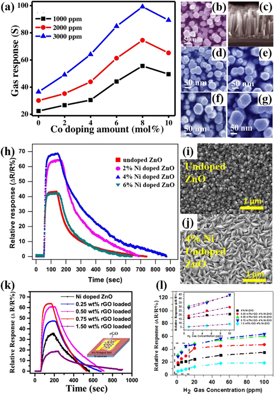
Figure 4. (a) Gas response vs Co doping content for different H2 concentration at 300 °C; Top view FESEM images of (b) ZnO and (d)–(g) 2, 4, 6 and 8 mol% Co content Co:ZnO NRs and (c) cross-sectional view of ZnO NRs.63 (h) Sensor's relative response for undoped and Ni- doped ZnO nanostructures sensor at 150 °C to 1% H2; Top view of FESEM images of (i) undoped and (j) 4% Ni-doped ZnO nanostructures.84 (k) Sensor's relative response for pristine and rGO-loaded ZnO for 100 ppm H2 gas at 150 °C; The inset shows the corresponding schematic diagram; (l) Response to different concentration of H2 of different rGO-loaded Ni doped ZnO sensors; the inset figure represents the enhanced linear-fitted hydrogen-gas-sensing response from 1 to 10 ppm.72
Download figure:
Standard image High-resolution imageDoping
Metal doping is one simple and useful method for enhancing the sensing property and conductivity of ZnO nanomaterials. The surface morphology, crystalline size, band gap, and structure of ZnO can be changed by metal doping route. This method increases the surface to volume ratio and creates more active sites for H2 gas adsorption due to the metal doping induced defects. Some metals such as Al,23 Mg,67 Co,49 Ni,84 Cd,83 In,85 Cu,86 and Ga50 have been used to dope ZnO TFs or other nanostructures, which replaces Zn2+ ions by introducing some structural defects such as oxygen vacancies or zinc vacancies. Due to the difference in atomic radius and chemical valence state between Zn and dopant, the lattice constant and energy band structure of ZnO are altered. The increased adsorption active sites and depletion layer width improves the H2 sensing performance.23,50,63,77
Sett et al. reported the H2 sensing characteristics of Co doped ZnO NRs synthesized by hydrothermal method. The diameter of Co doped ZnO NRs becomes larger from 42 nm to 66 nm with increasing the Co content from 0 to 8%, as shown in Figs. 4b–4g.63 It is found that compared to the undoped ZnO samples, 8 mol% Co doped ZnO NRs exhibit the highest and faster H2 gas response ability with a ∼5 fold response.
Yang et al. reported that Cd doping in ZnO NRs plays a key role in enhancing the performance of H2 sensor.83 The 2 at% Cd doped sample exhibits smallest d of ∼27 nm and optimal sensing properties, such as sensitivity of 1.67 to 500 ppm H2 at lower temperature of 80 °C with fast response time of 43 s.
Bhati et al. proved that the morphology of RF sputtering-derived ZnO TFs can be altered by Ni doping, as shown in Figs. 4i and 4j.84 The ZnO columnar structure with conical tips changes to the nanoplates of Ni doped ZnO. 4 at% Ni-doping produces more active sites for adsorbed oxygen on the surface of ZnO due to these formed structural defects. Therefore, for optimal 4 at% Ni-doped ZnO nanoplates, the charge transfer reactions easily occur on adsorbed oxygen ions, leading to the enhanced performance of H2 sensor with response of ∼69%b for 1% H2 at 150 °C (Fig. 4h).84
Based on this result, 0.75 wt% rGO was loaded on 4 at% Ni-doped ZnO nanostructure, showing optimal sensing response of ∼63.8%b at 100 ppm H2 at moderate operating temperature of 150 °C instead of ∼35.4%b for 4 at% Ni-doped ZnO nanoplates, as seen in Fig. 4k.72 Moreover, in Fig. 4l, this sensor exhibits marked response to 1 ppm-level H2 of 28.7% in comparison with 16.8% of Ni-doped ZnO nanoplates. More p−n Schottky junctions between rGO and Ni-doped ZnO and more active sites on rGO will be responsible for this.
Above all, most metal doped ZnO shows the enhanced surface to volume ratio and more gas active adsorption sites due to the produced structural defects such as oxygen vacancies,100 which is beneficial for the improvement of the sensing performance.23,63,101
Composite
The H2 sensing performance of ZnO can be enhanced by formation of composites including NCPs such as ZnO–SnO2 composite NFs51 and graphene/ZnO NCP,87 and core-shell (C–S) composites such as ZnO–SnO2 C–S NWs65 and ZnO@ZIF-8 C–S NRs.64 This can be attributed to the increased potential barrier height and surface depletion layer width, causing the significant resistance change after the introduction of H2 on the composite.51,102
An additional depletion layer is formed due to the difference in work function of two materials.103 In 0.9 SnO2-0.1 ZnO composite NFs, when nanograins of SnO2 contact with ZnO, electrons will be transferred from SnO2 to ZnO through the heterostructure until reaching the equilibrium of Fermi levels with reduced resistance of composite.51 In Fig. 5a, the high-resolution lattice fringes of several SnO2 and ZnO nanograins can be clearly observed in the SnO2–ZnO composite NFs, forming homo-interfaces and hetero-interfaces. Usually the grain size will affect the gas sensing ability. Grain size tuned H2 response characteristics are depicted in Fig. 5b. The smaller the grain sizes of SnO2–ZnO composite NFs such as 12 nm, the more the number of heterojunctions and homojuntions, resulting in the superior sensitivity of 3.6a to 30 ppb H2 at 350 °C (Fig. 5c).51

Figure 5. (a) Lattice-resolved TEM image of the SnO2-ZnO composite NF. (b) The responses of sensors fabricated with SnO2–ZnO composite NFs with different grain sizes to 0.1 ppm H2.51 (c) Dynamic resistance curves of sensors fabricated with SnO2-ZnO composite NFs with the grain size of 12 nm to 0.03 ppm of H2.51 (d) Sensing response vs operating temperature of ZnO and RGO/ZnO composite based sensors towards 200 ppm of H2.87 (e) A typical TEM image of 0.1 In2O3-loaded ZnO NFs (top); High-resolution TEM image (bottom). (f) Responses vs H2 gas concentration at 350 °C of 0.1 In2O3-loaded ZnO NFs gas sensors and Pd NP-functionalized 0.1 In2O3-loaded ZnO NFs gas sensors.80 (g) GI-X-ray diffraction (XRD) diffraction patterns and (h) schematic representation of the novel ZIF-8/Pd/ZnO NW sensor; (i) Calibration curves of bare ZnO, Pd/ZnO, and ZIF-8/Pd/ZnO NW gas sensors to 10, 30, and 50 ppm H2 gas at 200 °C.54
Download figure:
Standard image High-resolution imageIn addition, p-type NiO incorporated with n-type ZnO NFs forms the P-N heterojunction, which is more sensitive towards H2 sensing.21 Besides, it is noteworthy that higher amounts of oxygen ions could be easily adsorbed on the surface of the NiO, because Ni2+ ions are easily oxidized into Ni3+.21
Graphene offers an extensive 3D network to enhance the interconnectivity with ZnO, hence the optimal sensor performance towards H2 at lower temperature of 150 °C can be achieved using 1.2 wt% rGO/ZnO NCP, as shown in Fig. 5d.87 Due to the large specific surface area, high electronic mobility and low electrical noise, the defects and functional groups on the rGO surfaces act as high energy adsorption sites for the H2 molecules.87
As discribed previously, Pd NPs loaded on ZnO nanostructures significantly facilitate the H2 sensing capability of gas sensors.17 Herein, the Pd NPs-functionalized 0.1In2O3-0.9ZnO NFs were prepared by electrospinning and UV irradiation method.80 HRTEM image shows the microstructure of Pd NPs-functionalized 0.1In2O3-0.9ZnO NFs with clear lattice fringes from ZnO, In2O3, and Pd nanograins, as seen in Fig. 5e. The Pd NPs-functionalized 0.1In2O3-0.9ZnO NFs also present a strong response of 172a to 50 ppb H2 at 350 °C, much higher than 72a from 0.1In2O3-0.9ZnO NFs without Pd NPs' modification in Fig. 5f. The improved H2 response is attributed to the outstanding catalytic ability of Pd to H2, the formation of PdHx, and more junctions of Pd/ZnO, In2O3/ZnO, and ZnO/ZnO.80
In core–shell composite structure, it is found that the gas sensing capability has been improved significantly.54,64,90,92 Based on Kim's research group's review report on core–shell composite NWs or NRs gas sensors, gernerally when the shell thickness is comparable to the LD of the shell, the maximum response can be obtained due to a fully electron-depleted shell, leading to an enhanced gas sensing response.45 However, sometimes the optimal shell thickness is observed to be equal to 2LD, producing the highest gas response to reducing gas.45 For example, Park et al. reported that the H2 sensing properties of Nb2O5–ZnO C–S NW sensors is strongly dependent on the shell thickness (0–63 nm) of ZnO prepared by atomic layer deposition (ALD).92 The best response to 1% H2 at 300 °C is confirmed in Nb2O5–ZnO C–S NR sensors with a shell thickness of 46 nm, close to 2LD of ZnO. The reason lies in that apart from the surface depletion layer at outer surface of the shell, depletion layers also form at core–shell the interface, affecting the optimal shell thickness. So, the transfer of electrons though interface barrier is restrained, which increases the width of depletion layer and leads to an increased change in resistance and the enhanced sensitivity of H2 sensor.
Finally, a selective H2 gas sensor based on novel MOF ZIF-8 coated Pd NPs/ZnO NWs has been developed, as indicated in Fig. 5h.54 The GIXRD pattern in Fig. 5g and corresponding HRTEM (not shown here) has demonstrated that an ultrathin 2−3 nm thick ZIF-8 layer has covered homogeneously on the Pd NPs-decorated ZnO NW surface. The Pd NPs is beneficial to achieve maximal H2 signal responses, whereas the ZIF-8 coating enables for an excellent selectivity. As though the ZIF-8/Pd/ZnO NWs composite H2 sensor has a slight decreased sensitivity of 3.24a to low 10 ppm H2 at 200 °C than Pd NPs-decorated ZnO NWs with 4.26a, it displays enhanced response than pure ZnO NWs with 1.35a, as seen in Fig. 5i. More importantly, the introduction of ZIF-8 nanomembrance as a molecular sieve in Pd/ZnO NWs composite gets a superior selective H2 sensor, which will be discussed later.
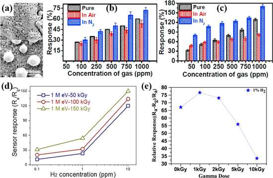
Figure 6. (a) SEM images of Au/ZnO TFs post-annealed in air (top) and N2 (bottom) at 600 °C; (b) Response of the pure and air/N2 annealed Au/ZnO TFs in dark and (c) under UV light to H2 of various concentrations at 250 °C.94 (d) Response of ZnO NF sensors irradiated at different e-beam doses to 0.1, 1, and 10 ppm H2 at 350 °C.47 (e) shows the relative response of ZnO NRs-based hydrogen sensors as a function of various un-irradiated and gamma-irradiated doses at 1% hydrogen concentrations.95
Download figure:
Standard image High-resolution image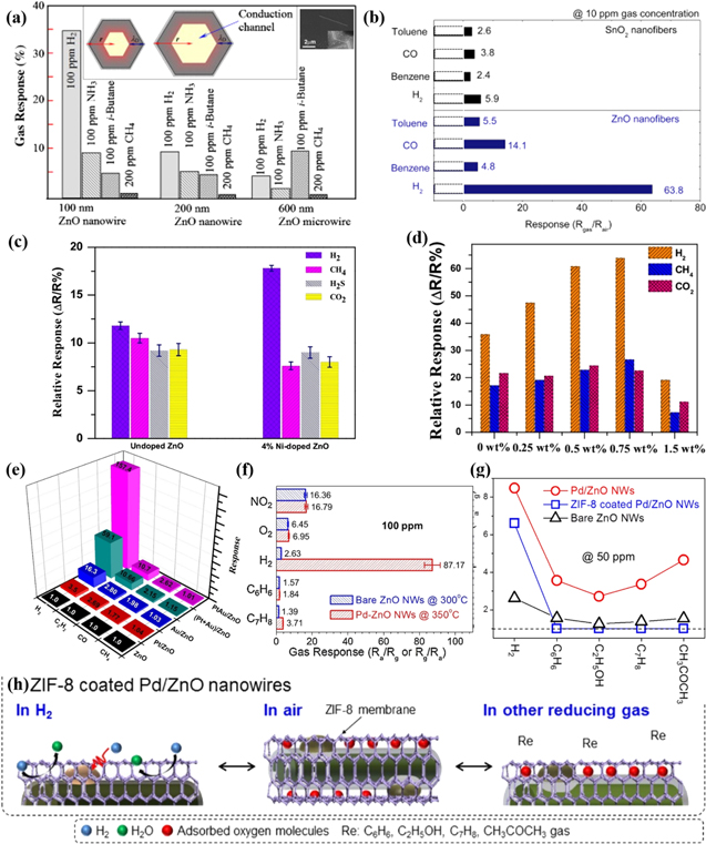
Figure 7. (a) Dependences of gas response for different diameter ZnO NW based sensors; Insert shows cross-sectional view of ZnO NWs with different radii (r) and same LD and conduction channel respectively; Transferred ZnO NW and insert shows a fabricated device based on a single NW of 100 nm in diameter.55 (b) Sensor responses to various reducing gases of SnO2 and ZnO NFs.66 (c) Selectivity test of undoped ZnO and 4% Ni doped ZnO for 5 ppm concentration at 150 °C operating temperature.84 (d) Selectivity histogram for sensors based on pristine and rGO-loaded Ni-doped ZnO nanostructures.72 (e) The gas sensing response of Pt, Au, Pt+Au and Pt-Au alloys NPs loaded on ZnO NRs to different reducing gases at 130 °C.78 (f) Selectivity histograms of the bare and Pd-functionalized ZnO NW sensors exposed to 100 ppm of different gases at their optimal temperatures.17 (g) Sensing responses of bare ZnO NW, Pd/ZnO NW and ZIF-8-coated Pd/ZnO NW gas sensors to 50 ppm of different gases at 200 °C. (h) Schematic representation of the sensing mechanisms for ZIF-8-coated Pd/ZnO NW sensors.54
Download figure:
Standard image High-resolution imagePost-treatment
Besides some strategies mentioned above, the post-treatment can be also used to improve the H2 sensing performance of ZnO, such as conventional post-annealing in optimal temperature or atmosphere and radiation technologies of γ irradiation, UV irradiation, and electron beam (EB) irradiation. These measures affect the morphology or grain sizes of ZnO or introduce some structural defects, which can be utilized to adjust the gas sensing properties.94,95,97,104
Kumar et al. found that Au NPs alter to Au spheres with diameter of 70–150 nm in the Au/ZnO TFs by post-annealed in N2 ambience at 600 °C, producing better H2 response than in air with much smaller Au NPs, as illustrated in Figs. 6a and 6b.94 Similarly, different grain sizes of 12.1 nm, 16.2 nm, and 22.3 nm in sol-gel-derived ZnO films can be obtained via varied post-annealing temperatures of 450 °C, 550 °C, and 650 °C in Ar, respectively.104 Among them, the device of Pd/450 °C-ZnO TFs has highest H2 response, which is ascribed to the largest surface to volume ratio and the most grain-boundaries because of the smallest grain sizes in ZnO TFs. However in some literature,94,96,97,103,104 the reported results on the post-anneal temperature and atmosphere impact on the H2 sensing performance of ZnO-based sensors are not consistent, even just on the contrary. It implies that the H2 sensing characteristics can be influenced by a lot of factors such as fabrication processing, gas sensor architecture and measurement.
Due to post-treatment such as radiation or post-annealing atmosphere, the structural defects especially oxygen vacancies are generated, and plenty of electron donors and adsorption sites are created.48,105–108 They will also affect the gas sensitivity of ZnO-based sensors. Recently Kim et al. studied the impact of EB radiation on ZnO NFs H2 sensor, indicating that the response to 100 ppb H2 of EB irradiated ZnO under optimal dose of 150 kGy is 1.64 times higher than that of non-radiated sample (see Fig.6d).47 The high response of 150a toward to 10 ppm H2 at 350 °C comes from its high surface area resulting from the one-dimensional nature of the ZnO NFs, the smaller grain size of ZnO, and the formation of surface defects by EB irradiation.47
UV-light enhanced high sensitive and selective H2 sensor based on spherical Au NPs on ZnO nano-structured TFs has also been confirmed, as indicated in Figs. 6b and 6c.94 The N2 post-annealed Au/ZnO TF sensor notably improves the sensing response under UV light illumination (365 nm) with about 172%c at 1000 ppm H2, twice magnitude of 80%c without UV light. UV light not only reduces the H2 detection limit from 100 ppm without UV light to 50 ppm, but also shortens the response/recovery time from 30 s/70 s to 15 s/49 s at 100 ppm.94 These results reveal that a combination of UV light illumination and post-annealing in N2 has a synergetic effect on the gas sensing performance of the sensor. The larger resistance change upon exposure to H2 gas molecules may be related to the photo-generated electron-hole pairs under UV light irradiation. The faster response/recovery time is attributed to higher UV light-induced desorption efficiency of oxygen adsorbates. However, UV-assisted H2 sensors might cause issues of health-safety and operation convenience, which has to be taken into consideration in the future practical application.
Selectivity of H2 Sensors Based on ZnO Nanostructures
Gas selectivity has always been a major issue for the resistive-type ZnO-based H2 sensors. From the view of the practical application, a sensor should present a rather high selectivity in the presence of other interfering gases such as ethanol (C2H5OH), CO, CH4, benzene (C6H6) or NO2. Different approaches have been employed to solve this problem, such as noble metal functionalization or sensitization, metal doping, nanocomposite or core–shell structure, molecular sieving effect, metallization effect of ZnO surface, irradiation, and synergistic effect of bimetallic alloy. Table IV summarizes recent progress on selectivity of ZnO nanosturctures-based H2 sensors.
Table IV. Summary of selectivity of various ZnO-based H2 sensors.
| System | Gas | T(°C) | Conc. (ppm) | Resp. | Selectivity (Reason) | References |
|---|---|---|---|---|---|---|
| ZnO NWs (D = 20–30 nm) | H2 | 150 | 1000 | 43a) | Poor | 58 |
| C2H5OH | 150 | 1000 | 300a) | |||
| Single ZnO NW (D = 100 nm) | H2 | RT | 100 | 34%b) | Good (More effective modulation of defects and diameter in single NW; Higher surface/volume ratio of NW) | 55 |
| NH3 | RT | 100 | 9%b) | |||
| i-Butane | RT | 100 | 5%b) | |||
| CH4 | RT | 200 | 1%b) | |||
| Single ZnO NW (D = 200 nm) | H2 | RT | 100 | 9%b) | Fair | 55 |
| NH3 | RT | 100 | 5.5%b) | |||
| i-Butane | RT | 100 | 5%b) | |||
| CH4 | RT | 200 | 1%b) | |||
| Single ZnO NW (D = 600 nm) | H2 | RT | 100 | 4%b) | Poor | 55 |
| NH3 | RT | 100 | 2%b) | |||
| i-Butane | RT | 100 | 9%b) | |||
| CH4 | RT | 200 | 1%b) | |||
| Aligned ZnO NRs (D = 10–30 nm) | H2 | 350 | 100 | 10.41a) | Poor | 65 |
| C2H5OH | 350 | 100 | 18.29a) | |||
| ZnO NTs (t = 42.7 nm) | H2 | 250 | 100 | 10.69a) | Poor | 39 |
| NH3 | 250 | 100 | ∼23a) | |||
| CH4 | 250 | 100 | ∼19a) | |||
| CO | 250 | 100 | 5a) | |||
| ZnO NFs (D = 100 nm, d = ∼30 nm) | H2 | 300 | 10 | 63.8a) | Better (Surface metallization of ZnO nanograins in NFs; Larger surface area) | 66 |
| CO | 300 | 10 | 14.1a) | |||
| C7H8 | 300 | 10 | 5.5a) | |||
| C6H6 | 300 | 10 | 4.8a) | |||
| Bare ZnO NFs (D = 100 nm) | H2 | 350 | 0.1 | 11.2a) | ibid | 48 |
| 0.6 wt% Pd/ZnO NFs (t = 5–10 nm; D = ∼100 nm) | H2 | 350 | 0.1 | 45.6a) | Very good (Metallization effect of ZnO; Catalytic activity of Pd) | 48 |
| C2H5OH | 350 | 0.1 | 9.43a) | |||
| C6H6 | 350 | 0.1 | 6.14a) | |||
| C7H8 | 350 | 0.1 | 5.99a) | |||
| CO | 350 | 0.1 | 3.18a) | |||
| Bare ZnO NPs (d < 25 nm) | H2 | 200 | 50 | 18a) | Very poor | 49 |
| Acetone | 200 | 10 | 55a) | |||
| C2H5OH | 200 | 10 | 80a) | |||
| Co-doped (20 at%) ZnO NPs (d = ∼25 nm) | H2 | 200 | 50 | 1.8b) | Fair (p-type behavior of Co-doped ZnO NPs) | 49 |
| Acetone | 200 | 10 | 2.1b) | |||
| C2H5OH | 200 | 10 | 1.75b) | |||
| CO | 200 | 5 | 1.5b) | |||
| NO2 | 200 | 5 | 1.3b) | |||
| CO2 | 200 | 10000 | 1.1b) | |||
| Bare ZnO NWs (D = 100 nm) | H2 | 300 | 100 | 2.63a) | Poor | 17 |
| C6H6 | 300 | 100 | 1.52a) | |||
| C7H8 | 300 | 100 | 1.37a) | |||
| NO2 | 300 | 100 | 16.36b) | |||
| O2 | 300 | 100 | ∼6.3b) | |||
| Pd/ZnO NWs (D = 100 nm, Pd surface coverage: 0.437) | H2 | 350 | 100 | 87.17a) | Very good (Pd functionalization; Metallization effect of ZnO) | 17 |
| C6H6 | 350 | 100 | 1.84a) | |||
| C7H8 | 350 | 100 | 3.71a) | |||
| NO2 | 350 | 100 | 16.79b) | |||
| O2 | 350 | 100 | 6.8b) | |||
| Single Au NPs/ZnO NWs (D = 120 nm, Au surface coverage: 6.4%, d ∼ 10–100 nm) | H2 | RT | 100 | 7.5a) | Excellent (Schottky contacts at interfaces of Au and ZnO; Metallization effect of ZnO) | 75 |
| Acetone | RT | 100 | <1.1a) | |||
| C2H5OH (CH3OH) | RT | 100 | <1.1a) | |||
| 2-Propanol | RT | 100 | <1.1b) | |||
| n-Butanol | RT | 100 | <1.1b) | |||
| Bare ZnO NRs (D = ∼200 nm) | H2 (C2H2, CO, CH4) | 130 | 250 | 1a) | Very poor | 78 |
| Pt NPs/ZnO NRs (Pt: d = 2.68 nm) | H2 | 130 | 250 | 3.5a) | Fair | 78 |
| C2H2 | 130 | 250 | 2.69a) | |||
| CO | 130 | 250 | 1.77a) | |||
| CH4 | 130 | 250 | 1.04a) | |||
| Au NPs/ZnO NRs (Au: d = 3.05 nm) | H2 | 130 | 250 | 16.3a) | Good (Catalysis of Au) | 78 |
| C2H2 | 130 | 250 | 2.80a) | |||
| CO | 130 | 250 | 1.98a) | |||
| CH4 | 130 | 250 | 1.03a) | |||
| (Pt+Au) NPs/ZnO NRs (Pt+Au: d = 2.72 nm) | H2 | 130 | 250 | 57.1a) | Very good (Catalysis of Pt and Au) | 78 |
| C2H2 | 130 | 250 | 10.66a) | |||
| CO | 130 | 250 | 2.15a) | |||
| CH4 | 130 | 250 | 1.15a) | |||
| Pt-Au alloys NPs/ZnO NRs (Pt:Au = 1:1; Pt-Au: d = 2.92 nm) | H2 | 130 | 250 | 157.4a) | Excellent (Synergetic and electronic effects of Pt-Au alloys) | 78 |
| C2H2 | 130 | 250 | 10.7a) | |||
| CO | 130 | 250 | 2.62a) | |||
| CH4 | 130 | 250 | 1.01a) | |||
| Pt/Pd C-S NPs/ZnO NRs | H2 | 100 | 10000 | 44%b) | Better (Synergetic and electronic effects of Pt-Au alloys) | 79 |
| CO | 100 | 10000 | 5%b) | |||
| CO2 | 100 | 10000 | 4%b) | |||
| NO2 | 100 | 10000 | −10.5%b' | |||
| O2 | 100 | 10000 | −5%b' | |||
| N2 | 100 | 10000 | 1.5%b) | |||
| 3 wt% In doped ZnO TFs (d = 14.3 nm; t = 300–400 nm) | H2 | 350 | 5 | 15%b) | Fair | 85 |
| CO | 350 | 5 | 14%b) | |||
| CH4 | 350 | 5 | 3%b) | |||
| 3 wt% Cu doped ZnO TFs (d = ∼18 nm; t = 300 nm) | H2 | 150 | 750 | 44.1%b) | Fair | 86 |
| CH4 | 150 | 750 | 32.6%b) | |||
| ZnO-SnO2 composite TFs (ZnO: D ∼ 500 nm NR; SnO2: 50–90 nm NP; Zn:Sn = 1:1; t ∼ 600–800 nm; T = 700 °C) | H2 | 150 | 10000 | 90%b) | Good (Surface EDL of ZnO and SnO2; Heterojunctions between ZnO and SnO2 grains) | 103 |
| CH4 | 150 | 10000 | 47%b) | |||
| CO | 150 | 10000 | 31%b) | |||
| 0.05NiO-0.95ZnO composite NFs (D = 125–150 nm; d≈15 nm) | H2 | 200 | 10 | 60%b) | Very good (Catalysis of NiO; Metallization effect of ZnO surface) | 21 |
| C6H6 | 200 | 10 | 9.4%b) | |||
| CO | 200 | 10 | 3.4%b) | |||
| 0.1SnO2−0.9ZnO composite NFs (D = 100 nm; d < 20 nm) | H2 | 300 | 50 ppb | 50a) | Excellent (Metallization effect of ZnO; Heterojunctions between ZnO and SnO2 grains) | 20 |
| NO2 | 300 | 50 ppb | 2.62b) | |||
| CO | 300 | 50 ppb | 1.57a) | |||
| 0.1ZnO-0.9SnO2 composite NFs (D = 90 nm, d = 12 nm) | H2 | 350 | 0.1 | 78a) | Very good (Large amount of heterojunctions and homojunctions in NFs; Hydrogen-induced metallization effect of grain boundaries of ZnO-SnO2; Smaller grain in NFs) | 51 |
| C2H5OH | 350 | 0.1 | 29.9a) | |||
| C6H6 | 350 | 0.1 | 19.7a) | |||
| CO | 350 | 0.1 | 12.2a) | |||
| C7H8 | 350 | 0.1 | 9.7a) | |||
| NO2 | 350 | 0.1 | 3.3b) | |||
| SO2 | 350 | 0.1 | 3.2a) | |||
| H2S (CO2) | 350 | 0.1 | 2.6(2.5)a) | |||
| 0.05Co3O4−0.95ZnO composite NFs (D ∼ 100 nm; d = 5–45 nm) | H2 | 300 | 10 | 133.65a) | Very good (Metallization of ZnO surface; p-n heterojunctions) | 89 |
| NO2 | 300 | 10 | 17.95b) | |||
| CO | 300 | 10 | 9.8a) | |||
| Pd/0.1In2O3-0.9ZnO composite NFs (D < 100 nm; oxide: d∼5–45 nm) | H2 | 350 | 0.05 | 152a) | Excellent (Pd-functionalization; Large amount of junctions in composite NFs; Zn metallization effect) | 80 |
| NO2 | 350 | 0.05 | 14.6b) | |||
| CO | 350 | 0.05 | 13.48a) | |||
| Raw ZnO NRs (D = 180 nm) | H2 | 250 | 50 | 2.15a) | Fair | 64 |
| CO | 250 | 50 | ∼1.62a) | |||
| ZnO@ZIF-8 core–shell NRs (D = 140 nm;ZIF-8:t∼110 nm) | H2 | 250 | 50 | 3.28a) | Good (Molecular sieving effect of ZIF-8;Increased specific surface area) | 64 |
| CO | 250 | 50 | ∼1.03a) | |||
| Bare ZnO NWs (D = 100 nm) | H2 | 200 | 50 | 2.6a) | Fair | 54 |
| Acetone | 200 | 50 | 1.8a) | |||
| C6H6 | 200 | 50 | 1.7a) | |||
| C7H8 | 200 | 50 | 1.5a) | |||
| C2H5OH | 200 | 50 | 1.3a) | |||
| Pd/ZnO NWs (D = 100 nm, Pd: 100 cycles) | H2 | 200 | 50 | 8.5a) | Good (Pd-functionalization) | 54 |
| Acetone | 200 | 50 | 4.7a) | |||
| C6H6 | 200 | 50 | 3.6a) | |||
| C7H8 | 200 | 50 | 3.4a) | |||
| C2H5OH | 200 | 50 | 2.7a) | |||
| ZIF-8/Pd/ZnO composite NWs (ZIF-8:t = 2–3 nm) | H2 | 200 | 50 | 6.6a) | Excellent (Synergistic effect of Pd NPs and molecular sieve membranes) | 54 |
| Acetone (C6H6) | 200 | 50 | 1a) | |||
| C2H5OH(C7H8) | 200 | 50 | 1a) | |||
| Pristene ZnO TFs (t = 600 nm, d ∼ 100–150 nm; surface: conical tips) | H2 | 150 | 5 | 11.8%b) | Poor | 84 |
| CH4 | 150 | 5 | 10.5%b) | |||
| CO2 | 150 | 5 | 9.33%b) | |||
| H2S | 150 | 5 | 9.25%b) | |||
| 4 at% Ni doped ZnO nanoplates (t ∼ 1 μm, grain: ∼ 130 nm × 300 nm) | H2 | 150 | 5 | 17.8%b) | Good (Increased surface area; More active sites induced by structural defects) | 84 |
| CH4 | 150 | 5 | 7.4%b) | |||
| CO2 | 150 | 5 | 8.2%b) | |||
| H2S | 150 | 5 | 9.11%b) | |||
| 4 at% Ni doped ZnO nanoplates (ibid) | H2 | 150 | 100 | 35.4%b) | Good | 72 |
| CH4 | 150 | 100 | 16.9%b) | |||
| CO2 | 150 | 100 | 21.2%b) | |||
| 0.75 wt% rGO/4 at% Ni doped ZnO nanoplates | H2 | 150 | 100 | 63.8%b) | Better (Synergistic effect of more p−n Schottky junctions with larger barrier height and more active sites on rGO) | 72 |
| CH4 | 150 | 100 | 26.5%b) | |||
| CO2 | 150 | 100 | 22.5%b) | |||
| 150 kGy EB irradiation of ZnO NFs (D = 120 nm; d = ∼5–10 nm) | H2 | 350 | 10 | 150a) | Excellent (Zn metallization effect; Increased oxygen vacancies; Enhanced BET surface area) | 47 |
| C2H5OH | 350 | 10 | 10.53a) | |||
| C7H8 | 350 | 10 | 2.52a) | |||
| CO | 350 | 10 | 1.41a) | |||
| C6H6 | 350 | 10 | 1.33a) | |||
| UV irradiation Au/1.2 wt% rGO/ZnO NCP | H2 | RT | 800 | 83%b) | Excellent (High surface area; Increased oxygen vacancies; Work function difference in Au and ZnO; Formation of rGO/ZnO heterostructure; Weak adsorption of other gases at RT) | 93 |
| C4H10 | RT | 50000 | 7%b) | |||
| CH4 | RT | 1000 | 21%b) | |||
| CO2 | RT | 1000 | 3%b) | |||
| NH3 | RT | 1000 | 19%b) | |||
| O2 | RT | 15000 | 12%b) | |||
| Au NP/ZnO TFs without UV irradiation (Au spheres: d = 70–150 nm) | H2 | 250 | 1000 | 0.72b) | Fair | 94 |
| C2H5OH | 250 | 1000 | 0.29b) | |||
| CH4 | 250 | 1000 | 0.25b) | |||
| CO2 | 250 | 1000 | 0.24b) | |||
| CO | 250 | 1000 | 0.21b) | |||
| H2S | 250 | 1000 | 0.12b) | |||
| SO2 | 250 | 1000 | 0.11b) | |||
| NO2 | 250 | 1000 | 0.46b) | |||
| Au NP/ZnO TFs with UV irradiation (Au spheres: d = 70–150 nm) | H2 | 250 | 1000 | 1.72b) | Good | 94 |
| C2H5OH | 250 | 1000 | 0.45b) | |||
| CH4 | 250 | 1000 | 0.35b) | |||
| CO2 | 250 | 1000 | 0.3b) | |||
| CO | 250 | 1000 | 0.48b) | |||
| H2S | 250 | 1000 | 0.19b) | |||
| SO2 | 250 | 1000 | 0.31b) | |||
| NO2 | 250 | 1000 | 0.66b) |
Notes: a') S = Rg/Ra. b'S = (Rg-Ra)/Ra. a)S = Ra/Rg. b)S = (Ra-Rg)/Ra. D refers to diameter of NWs, NRs, or NFs. T refers to annealed temperature. The other symbols are the same as in Tables II and III.
As seen from Table IV, most pristine ZnO nanostructures-based sensors, such as NPs, NWs, NRs, NTs, and TFs, have poor selectivity for H2 in the presence of interfering gases such as C2H5OH, acetone, i-butane, CH4, C2H2, CO2, CO, H2S, and NO2. However, very few exceptions can be observed in single ZnO NW-based nanoscale sensor and electrospinning-derived ZnO NFs H2 sensor.55,66
The effect of diameter of single crystal ZnO NW sensor on the H2 response and selectivity at RT is shown in Fig. 7a and Table IV.55 It can be seen that the nanoscale sensor based on individual ZnO NW with diameter of 100 nm have better selectivity for H2 when reducing gases of NH3, i-butane, and CH4 exist. As the diameter of ZnO NWs increases from 100 nm to 200 nm and 600 nm, the H2 response evidently decreases and the H2 selectivity becomes worse. For example, the corresponding value of SH2/Si-butane reduces from 6.8 (D = 100 nm) to 1.8 (D = 200 nm) and 0.44 (D = 600 nm). Lupan et al. attributed this to the diameter of ZnO NW on the influence of surface to volume ratio and surface defect concentration.55
Katoch et al.66 made a comparative study on the selectivity of SnO2 and ZnO NFs to H2, CO, C6H6, and toluene (C7H8), as illustrated in Fig. 7b. Compared to SnO2 NFs, ZnO NFs have unmistakable H2 selectivity due to the Zn metallization effect on the surface of ZnO nanograins in NFs. Although SnO2 NFs consist of 30 nm nanograins similar to ZnO ones, it lacks the reaction from SnO2 to Sn on the nanograin surface induced by H2. As a result, the value of SH2/SCO of SnO2 NFs is only 1.55, however that of ZnO is up to 4.52.
Generally speaking, the selectivity to H2 of pristine ZnO-based gas sensors can be improved by some measures such as doping and surface modification. As mentioned earlier in Figs. 4h–4i, the 4 at% Ni-doped ZnO nanoplates and 0.75 wt% rGO loaded 4 at% Ni doped ZnO nanoplates show enhanced H2 sensitivity than without Ni-doped and rGO-decorated ZnO samples.72,84 Figures 7c and 7d illustrate the selectivity of 3 kinds of samples.72,84 It can be seen that undoped ZnO TFs has worse selectivity to H2, CH4, CO2, and H2S. The 4 at% Ni-doping and 0.75 wt% rGO surface decoration improves the selectivity to H2 over other reducing gases. For instance, the SH2/SCH4 of bare ZnO films is merely 1.12. After the Ni-doping, it becomes 2.41. Similar result occurs in rGO loaded doped ZnO sample with higher sensitivity, revealing the helpful role of Ni-doping and rGO surface modification on the selectivity of H2 sensors.
Apart from rGO decoration, modification of noble metals is one of the most effective methods to reduce the energy required for the gas adsorption/disorption reaction. Fan et al. investigated the selective properties to H2 of Pt, Au, Pt+Au and Pt-Au alloys NPs loaded on ZnO NRs in presentence of C2H2, CO, and CH4.78 The values of SH2/SCO are 60.07, 27.49, 8.23, 1.98, and 1 for the Pt-Au/ZnO, (Pt+Au)/ZnO, Au/ZnO, Pt/ZnO, and bare ZnO NRs calculated from the data in Fig. 7e, respectively. Individual Pt and Au NPs play a valid role in increasing the H2 selectivity of ZnO NRs. Furthermore, the mixture of Pt and Au NPs produces much better H2 selectivity than single Pt or Au NPs. However, the Pt-Au bimetallic NPs show the best H2 selectivity over C2H2, CO, and CH4 because the adsorption of H2 onto the Pt-Au NPs is more favorable than that on monometallic.
In addition, Pd functionalized ZnO nanostructures are highly selective for H2 detection due to the formation of Pd hydride (PdHx),17,48,54 resulting in the great improvement in the selectivity of the H2 sensors. In Fig. 7f, the values of SH2/SC6H6 are 1.68 and 47.38 before and after Pd functionalized ZnO NWs.17 Similarly, individual Au NPs decorated ZnO NW also exhibits stronger H2 selectivity with negligible response to other interfering gases such as acetone, C2H5OH, CH3OH, 2-propanol, n-butanol.75
Another very effective method for improving the selectivity of H2 sensor can be achieved by choosing metal organic frameworks (MOFs) with different pore sizes as a molecular sieve.64 Weber et al. reported that the selectivity of Pd-decorated ZnO NWs can be notably improved by the introduction of ZIF-8 MOF nanomembranes.54 The values of SH2/Sacetone are increased from 1.44 for bare ZnO NWs to 1.80 for Pd NPs/ZnO NWs and 6.6 for ZIF-8/Pd NPs/ZnO NWs by adding Pd and ZIF-8, respectively, as shown in Fig. 7g. The related mechanism is illustrated in Fig. 7h. The ZIF-8 membranes with micropores size of 3.4 Å only allow smaller H2 molecules of 2.9 Å to pass through the membranes layer instead of other larger gas molecules such as acetone, C6H6, C7H8, and C2H5OH.54 Thus, the ZIF-8/Pd/ZnO NWs composite H2 sensor displays admirable selectivity than pure ZnO NWs and Pd NPs-decorated ZnO NWs.54
The aforementioned pure ZnO NFs exhibit better selectivity to 10 ppm H2 at higher work temperature of 300 °C. Based on this foundation, Kim's research group has performed a series of in-depth improvement studies on the H2 selectivity of ZnO-based nanocomposite NFs using SnO2,20,51 NiO,21 Co3O4,89 and Pd NPs decorated In2O3,80 as indicated in Figs. 8a–8e. Using CO as an interfering gas, the value of SH2/SCO for pristine ZnO NFs (300 °C, 10 ppm H2), 0.9SnO2-0.1ZnO NFs (350 °C, 0.1 ppm H2), 0.1SnO2-0.9ZnO NFs (300 °C, 0.05 ppm H2), 0.05Co3O4-0.95ZnO NFs (300 °C, 10 ppm H2), 0.05NiO-0.95ZnO NFs (200 °C, 10 ppm H2), and Pd NPs/0.1In2O3–0.9ZnO NFs (350 °C, 0.05 ppm H2) is 4.52, 6.39, 31.85, 13.64,17.65, and 11.28, respectively. The experimental results reveal that the ZnO nanocomposite NFs exhibit evidently enhanced H2 selectivity over other interfering gases, especially for 0.1SnO2-0.9ZnO NFs sample with an outstanding 50 ppb-level H2 selectivity at 300 °C owing to the formation of heterojunctions between ZnO and SnO2 grains and the metallization effect of ZnO nanograins.20 Moreover, Pd-functionalized 0.1In2O3–0.9ZnO NFs also display 50 ppb-level H2 selectivity with superior sensitivity up to 172a at 350 °C, which is attributed to the synergetic effect of the Pd catalytical activity, large amount of junctions in composite NFs, and Zn metallization effect.80
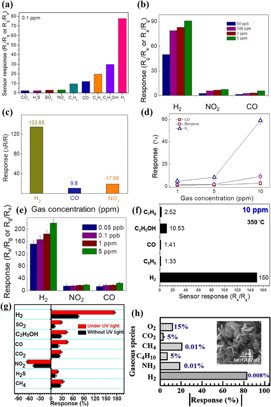
Figure 8. (a) Summary of sensor responses of the sensors fabricated with SnO2–ZnO composite NFs to 0.1 ppm various gas.51 (b) Response to different gas of the 0.1 SnO2-loaded ZnO NFs gas sensor at 300 °C.20 (c) Selectivity pattern of the 0.95 ZnO–0.05 Co3O4 NF sensor toward 10 ppm H2, CO and NO2 gases at 300 °C.89 (d) Response vs gas concentration of 0.05 wt% NiO-loaded ZnO NF gas sensor for 1, 5, and 10 ppm concentrations of H2, CO, and C6H6 gases at 200 °C.21 (e) Selectivity histogram of Pd NP-functionalized 0.1 In2O3-loaded ZnO NFs gas sensor.80 (f) Histogram of selectivity of 150-kGy-irradiated ZnO NF sensor toward different gases (10 ppm) at 350 °C.47 (g) Cross-sensitive response of the sensor based on the N2 post-annealed Au/ZnO TF to various gases (1000 ppm) at 250 °C under dark and UV light.94 (h) Selectivity test of Au/rGO/ZnO sensor toward 500 ppm of H2 under UV irradiation at RT and insert shows the SEM micrography of Au/rGO/ZnO.93
Download figure:
Standard image High-resolution image
In addition, it is found that the EB and UV irradiation can also enhance the H2 selectivity of ZnO-based has sensors, as seen in Figs. 8f–8h.47,93,94 After 150 kGy EB irradiation, the value of SH2/SCO of ZnO NFs can be remarkably increased to 106.38 at 10 ppm H2 and 350 °C, which is related to enhanced oxygen vacancies and BET specific surface area produced by EB-irradiation and the transition from ZnO to Zn.47 For Au NPs-decorated ZnO TFs, UV illumination at 365 nm may slightly ameliorate the H2 selectivity to reducing gases of SO2, CO, CO2, C2H5OH, CH4, and H2S, and oxidizing of NO2 at 1000 ppm H2 and 250 °C, but not very evident in Fig. 8g.94 For Au decorated rGO/ZnO NCPs, UV irradiation shows superior H2 selectivity to C4H10, CH4, CO2, NH3, and O2 at RT, as depicted in Fig. 8h.93 The UV light enhancement of gas-sensing performance can be ascribed to the drop of activation energy between the surface of the sensor and H2 gas.
Above all, ZnO is a suitable and excellent sensing material for the detection of H2 gas. However, the pristine ZnO suffers from a limited selectivity owing to the good responses to other interfering gases. Some effective and viable strategies such as the Pd-functionalization,17 the formation of metal oxide-ZnO nanocomposite NFs,20 combination of several approaches, e.g. Pt-Au alloys NPs modified ZnO NRs,78 Pd-functionalized 0.1In2O3-0.9ZnO NFs,80 ZIF-8 encapsulated Pd/ZnO NWs,54 and UV-activated Au decorated rGO/ZnO NCP,93 have been explored to circumvent this problem. A few gas sensors with admirable H2 selectivity have been achieved. However, continuous efforts are needed to obtain selective H2 sensor with superior selectivity and extremely low detection limit operated at RT.
Conclusions and Outlook
With an aim to improve the performance of H2 sensor based on ZnO nanostructures, this review paper compares the sensing properties and related mechanism of various kinds of pristine ZnO nanostructures for H2 detection. Furthermore, some improvement strategies of H2 sensing performance based on ZnO nanostructures sensors are focused and summarized. Especially, the selectivity of ZnO nanosturctures-based H2 sensors in the presence of interfering gases is strengthened and discussed.
A series of researches indicate that the H2 sensing activity of ZnO can be improved by increasing the active sites, widening the depletion region, and enhancing grain boundary barrier. In terms of nanostructures, the grain sizes in NPs, NFs and TFs, the diameter of NWs or NRs, the shell thickness of NTs have significant effect on the sensing capability of H2 sensor based on pure ZnO nanostructures according to surface charge layer model related to LD. For polycrystalline ZnO material, grain boundary barrier model has to be considered. Different from other metal oxide, e.g. SnO2, the H2-induced metallization effect of ZnO at high temperature plays a crucial role in improving the sensitivity and selectivity of ZnO-based H2 sensors along with valence control model.
At present, the H2 sensing activity of individual single-crystal ZnO NW-based sensor at RT has been confirmed by using Pt/ZnO Schottky diode structure.55 It is attributed to low barrier height of 0.42 V in ZnO/Pt Schottky junction and higher surface-to-volume ratio of ZnO NW surface. ZnO NTs has more adsorption sites at inner and outer sides of hollow NTs, leading to stronger response to H2. But hollow structure with high aspect ratio will also affect the gas diffusivity with longer recovery time.39 Recently, the superior H2 sensing characteristics of pure ZnO NFs sensors have been reported at 10 ppm H2 and 350 °C,66 which is related to the existence of numerous nanograins and porous structure in NFs. However, the higher work temperature impeding the practical application due to the power consumption issue.
Therefore, although ZnO is an outstanding H2 sensing material with high response, good stability, low cost, and extremely abundant nanostructures, pristine ZnO suffers from drawbacks such as higher operation temperature, worse selectivity, longer response/recovery time, and higher limit of detection. Quite a few approaches have been explored to enhance the performance of ZnO-based H2 sensors such as surface modification, doping, composite, and post-treatment. Among these strategies, noble metal modification and nanocomposite fabrication are two kind of effective and simple method for improving the H2 sensing ability, especially Pd NPs decoration17,29 and ZnO composite NFs' formation.21,51,80 In addition, bimetallic NPs such as Pt-Au alloy exhibit better H2 sensing responses compare to individual metal ones owing to the synergistic effect.78 Some studies have combined two or three improvement routes to achieve excellent performance of ZnO based H2 sensors, e.g. Pd NPs-functionalized 0.1In2O3-0.9ZnO NFs for ultra low detection of 50-ppb H2, ZIF-8 coated Pd NPs decorated ZnO NWs for superior selectivity to H2, Pt/Pd core–shell NPs decorated ZnO NRs for ultrafast response of 5 s at 100 °C,79 and Au loaded 1.2 wt% rGO/ZnO NCP with UV irradiation for higher sensitivity and selectivity at RT.54,79,80,93
Above all, by extensive and intensive researches, some significant progress has been achieved for resistive-type ZnO nanostructures-based H2 sensors such as higher response, lower work temperature even at RT, faster response time, lower detection concentration, longer durability, and better selectivity. However, until now, the development of ZnO-based H2 sensor with excellent comprehensive performance, which can simultaneously meet with outstanding sensitivity, superior selectivity and extremely low detection limit operated at RT, is still a tough challenge. Sometimes, we have to reach certain trade-off between sensitivity, selectivity, and work temperature.
At present, the sensing activity of ZnO based H2 sensor at RT is still evidently worse. They usually need to work at high temperature, which causes the higher power consumption with inconvenience. Therefore, it is necessary and urgent to improve the H2 sensing performance at RT. Recently, H2 gas can be detected at RT by using two dimension electron gas in the interface of Al2O3/TiO2 ultra-thin film derived by novel atomic layer deposition,109 which is an enlightenment of ZnO based H2 sensor. Atomic layer deposition (ALD) is a novel materials fabrication method compatible with the semiconductor technology. The unique self-limiting and self-saturation reaction mechanism enables the deposited nanomaterials with large area uniformity, simple and precise thickness control, excellent three-dimensional conformality and low deposition temperature.110 It may be a suitable method for the preparation of H2 sensing materials, such as core–shell structures, nanotubes, nanolaminate, and metal nanocrystals, with controlled thickness even at sub-nanometer. In future, the highly sensitive, flexible and wearable H2 sensor will be fabricated by using ZnO based gas sensor combined with the advanced micro-electro-mechanical system (MEMS) and other preparation techniques such as ALD.
In summary, at the tipping point the development of ZnO nanostructures-based H2 sensors is facing tremendous opportunities and challenges ahead. It is expected that ZnO nanostructures-based H2 sensors have promising futures and prospects in the Internet of Things, energy fields, environmental protection and safety through persistent efforts of academia and industry.
Acknowledgments
This work was supported in by the National Science Foundation of China (grant No. 51571111, 51721001, 51802150) and Jiangsu Province (BK20161397 and BK20170645), and a grant from the State Key Program for Basic Research of China (2015CB921203).