Abstract
Room-temperature Si/Si wafer direct bonding has been achieved successfully without wet chemistry treatment as well as no requiring annealing. Very strong bonding strength of Si/Si pairs, close to the bulk-fracture strength of silicon, is demonstrated at room temperature thanks to adding small amount of carbon tetrafluoride (CF4) into oxygen plasma treatment. The surface energies of bonded Si/Si wafer pairs were influenced by plasma treatment parameters. Moreover, the wafer surfaces and the bonding interfaces are analyzed to explore the bonding mechanism. Adding small amount of CF4 into O2 plasma does not etch the Si surface in a short time (∼60 s), but it renders fluorinated oxide grown on the Si surface, which should be less hydrophilic than the surface treated by O2 plasma. Therefore, fewer water molecules at bonding interface may be prone to produce many covalent bonds via polymerization reaction and result in strong bonding at room temperature.
Export citation and abstract BibTeX RIS
Conventional hydrophilic and hydrophobic bonding processes involve high-temperature annealing above 700–1000°C that would cause undesirable effect on the bonded structure and devices.1 To realize the annealing step at low temperature, many efforts have been made in recent years. Plasma is a partially ionized gas containing charged and neutral particles, which include positive and negative ions, neutral radicals, atoms or molecules, and UV radiations. The plasma can induce physical and chemical effect on the wafer surfaces. Surface activation prior to bonding has been carried out using dry plasma treatment. It is a convenient and low-cost solution for decreasing the annealing temperature. However, after O2, N2, or Ar plasma treatment, low-temperature annealing (200–400°C) is generally necessary to strengthen the bonding.2 Although plasma activation followed by wet chemistry treatment can enhance the bonding strength, voids are easily raised at bonding interfaces during the annealing step.3 Furthermore, combined plasma and wet chemistry treatment (e.g. using HF acid and NH4OH dips) has been reported enabling strong bonding even at room temperature after storage in air for 40 h.4, 5 This bonding method, although able to work well for many applications, requires multiple treatment steps that complicate the fabrication process. Moreover, the process complexity of plasma activation followed by wet chemistry cleaning is undesirable to microfluidics and biomedical devices.6 Alternatively, several vacuum wafer bonding methods have been reported for achieving reliable bonding even at room temperature, such as surface activated bonding,7 and ultra-high vacuum bonding.8 They are capable of room-temperature bonding without annealing but the whole bonding process requires high-vacuum condition (<10−5 Pa) that makes these processes expensive and less applicable for mass production. It thus seems very attractive to develop a wafer bonding method enabling (i) reliable bonding at room temperature without requiring annealing step, (ii) void-free at bonding interfaces, (iii) low-cost without requiring high-vacuum system, and (iv) facile treatment step prior to bonding.
In this paper, we describe a facile room temperature bonding process in air without requiring wet chemistry treatment and annealing process. Tetrafluoromethane (CF4), alternatively known as carbon tetrafluoride, is the simplest fluorocarbon and nontoxic gas. CF4 plasma has been extensively used for dry etching of silicon and silicon oxide. But very limit work has been done to study the effects of CF4 gas or its mixture plasma on wafer bonding. In this work, we speculate that O2 plasma containing some amount of CF4 treatment prior to bonding is possible to improve the bonding strength at room temperature. The plasma treatment parameters are optimized in this work. Moreover, the physical effects on surface roughness and etching depth are investigated using atomic force microscopy (AFM) and surface profiler. And the chemical states of surfaces are analyzed by x-ray photoelectron spectroscopy (XPS). In addition, Si/Si bonding interfaces are characterized by transmission electron microscopy (TEM) as well as Fourier transform infrared (FT-IR) spectroscopy. The bonding mechanism is also explored in this paper.
Experimental
Commercially available 4-in. silicon wafers were used in this work. All the wafers are p-type, (100)-oriented, one-side-polished, Czochralsky (CZ)-grown bare wafers. The thickness is 525 μm. It is known that a native oxide of a few Å is grown on the silicon surfaces at room temperature exposed to air. Thus the bonding of two silicon wafers is actually a bonding of two native-oxide-layers covered silicon wafers. But they are still called shortly as "Si/Si bonding" to simplify the words hereinafter.
In our experiments, the two wafers were loaded into the load lock chamber and then were transferred to plasma chamber by a transfer arm. The pressure of vacuum background is ∼0.1 Pa. The gas [O2 or (O2 + CF4) mixture gas)] was introduced into the plasma chamber at a pressure of 50 Pa. Reactive ion etching (RIE) plasma is generated by discharge between the ion-trapping metal plate and the radio frequency (RF) electrode.9 The frequency for RF discharge is 13.56 MHz and the discharge power is in the range of 0–400 W (adjustable). In this work, all wafer surfaces were treated with RIE plasma for 60 s. After that, the two wafers were taken out of the plasma chamber exposed to air and placed on the surface humidity controlled plate for 2–3 min at relative humidity ≈75%. Then they were brought into contact at room temperature in air. By locally applying a slight pressure, the bonded area spreads laterally over a large area within a few seconds. After contacting in air, the temporary bonded wafer pairs were cold rolled under 75 kgf in air to remove unbonded area. The bonded wafer pairs were stored at room temperature in air 24 h to saturate the bonding strength.
The surface energy of bonded wafer pairs is measured using the Maszara razor blade test (crack opening method). This is the most convenient method of determining the surface energy of the bonded wafer pairs.10 A 100-μm-thick razor blade was inserted at the bonding interfaces, and the crack propagation length is measured using a real-time IR imaging system. The surface energy (γ) is calculated on the basis of the following equation
where E is Young's modulus (1.30 × 10¹¹ Pa for Si), tb is the blade thickness, tw is the wafer thickness, and L is the crack propagation length.
To further confirm the bonding strength, some bonded wafer pairs were diced into 10 mm × 10 mm pieces. And small samples were taken randomly from each diced bonded pair and attached to metal fixtures (jigs) with glue for the pulling tensile test. The bonding strength was measured using a tensile pulling tester (AGS-1 kNG), which was made by Shimadzu Corporation. The pull speed was 0.5 mm/min and the bonding strength can be calculated as the ratio of breaking force to the sample area.
A commercially available AFM (SPI-3800N from Seiko Instrument in dynamic force mode), was used to measure the surface roughness of the wafer surfaces. XPS studies on silicon surface were performed to understand the effect of the fluorine containing plasma. XPS spectra were taken using a JEOL JSP-9200T spectrometer with Mg Kα (1253.6 eV) radiation source. Cross-sectional high-resolution transmission electron microscopy (HRTEM) investigation was made to characterize the bonding interface.
Results and Discussion
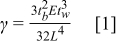
The effects of CF4 flow on Si/Si bonding strength were investigated. The CF4 gas with different flows was mixed with O2 500 sccm flow for plasma activation respectively. The RIE plasma was generated by discharge power of 200 W at the chamber pressure of 50 Pa. Figure 1 shows surface energy of Si/Si bonded wafer pair as a function of CF4 gas in (O2 + CF4) plasma treatment prior to contact. CF4 with 0 sccm flow refers to using O2 plasma treatment alone. Fluorine concentration in plasmas gas that corresponding to CF4 flow is indicated in Fig. 1. By adding small amount of CF4 to O2 plasma, the surface energy increases significantly. For the CF4 flow in the range of 1–1.5 sccm, very strong bonding energies are achieved even at room temperature. Particularly, the surface energy for the wafers prepared by (O2 + CF4 1.25 sccm) plasma treatment is a factor of 4 higher than by O2 plasma (∼0.6 J/m2). The average value reaches ∼2.4 J/m2, very close to the bulk fracture strength of silicon (∼2.5 J/m2). In most cases, we thus cannot insert razor blades into the bonding interface without breaking the bonded pairs. On the other hand, the surface energy decreases dramatically for the CF4 flow ranging from 2.0 to 5.0 sccm.
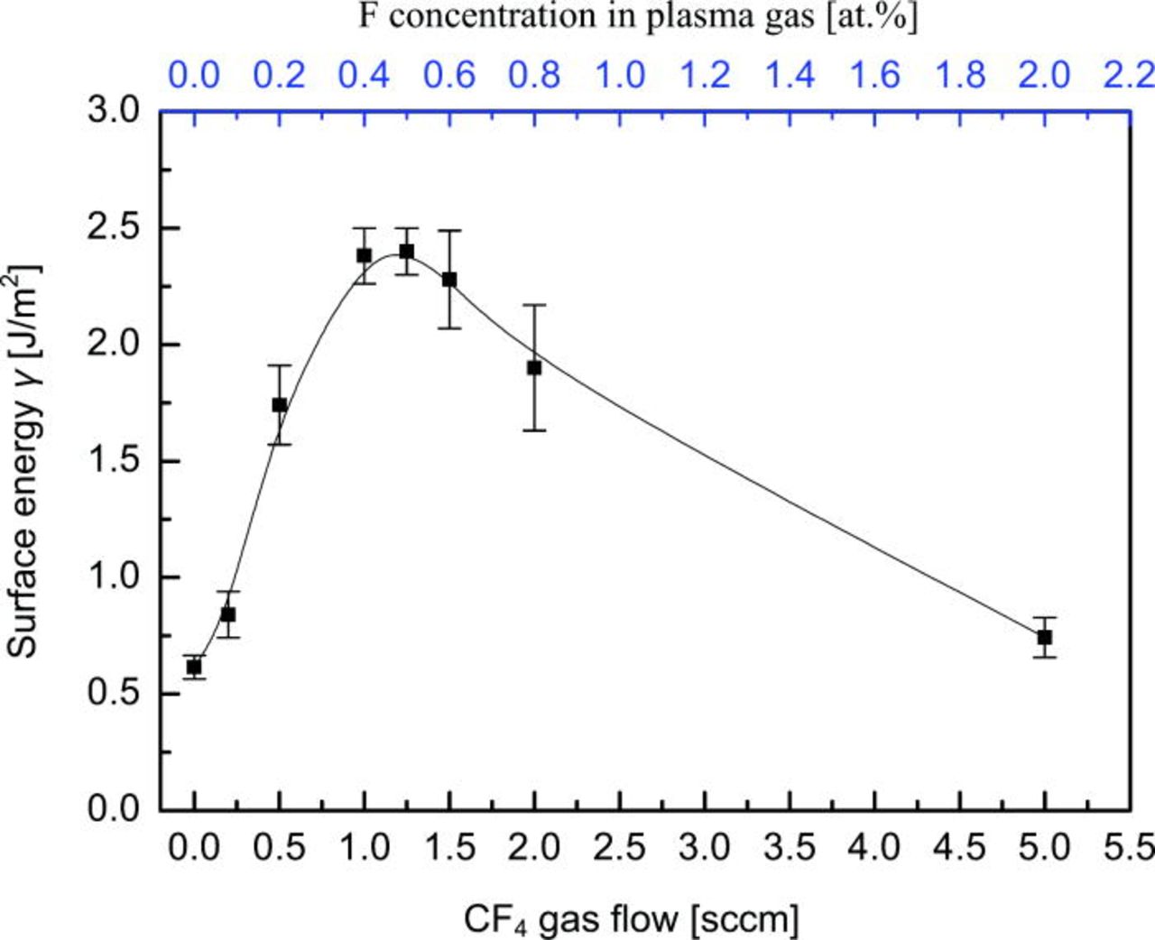
Figure 1. (Color online) Surface energy of bonded wafers pairs vs CF4 gas in (O2 + CF4) plasma treatment prior to bonding. All samples were bonded in air and stored for 24 h at room temperature to saturate the surface energy.
The pull tensile test was performed to inspect the bonding strength. The results are shown in Table I. The bonded sample treated by (O2 + CF4 1.25 sccm) plasma shows the strongest bonding strength ∼14.7 MPa and the fracture occurred at the silicon bulk at room temperature. For the bonded pairs prepared by O2 plasma treatment alone, the bonding strength is much lower than by fluorine containing plasma treatment and the fracture took place at the bonding interface.
Table I. Bonding strength at room temperature in the pull tensile test.
| Treatment (60 s) | Bonding strength (MPa) | Fracture |
|---|---|---|
| O2 plasma | 5.7 ± 0.4 | Interface |
| (O2 + CF4 1.0 sccm) plasma | 13.4 ± 0.8 | Bulk/glue |
| (O2+ CF4 1.25 sccm) plasma | 14.6 ± 2.7 | Bulk |
| (O2 + CF4 1.5 sccm) plasma | 11.3 ± 3.8 | Bulk/interface |
The effects of discharge power on Si/Si bonding were investigated. Figure 3 shows surface energy as a function of discharge power for (O2 + CF4 1.25 sccm) plasma treatment for 60 s. For discharge power = 40 W, the surface energy is fairly low. It seems that the gas was not discharged effectively at this condition. When the powers were between 200 and 300 W, it is peak value for the surface energy.
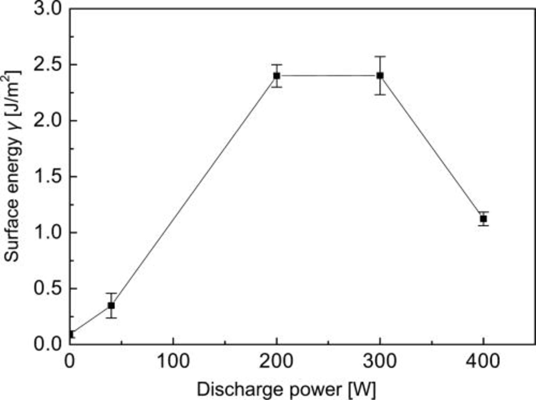
Figure 3. Surface energy bonded wafers pairs as a function of discharge power for (O2+ CF4 1.25 sccm) plasma treatment for 60 s.
In addition, the effects of plasma treatment time, bonding ambient (in air and vacuum) and storage ambient were also investigated respectively. We found the optimized plasma treatment parameters and selected process flow for Si/Si bonding is shown and highlighted with red color in Fig. 4. Compared to other plasma treatments, CF4 containing O2 RIE plasma enhances the bonding strength of Si/Si pairs significantly. The surface energy of Si/Si close to bulk-fracture strength of silicon is achieved at room temperature. CF4 gas flow determining the amount of fluorine in plasma is an important factor for bonding. In our experiments, the optimum CF4 flow is 1.25 sccm, which is fixed hereinafter. Moreover, the bonding strength is also influenced by the environment of bonding and storage.
Figure 4. (Color online) Optimized treatment parameters and selected process flow (highlighted with red color) for room-temperature bonding of Si/Si.
The measured root mean square (RMS) surface roughnesses of silicon surface before and after plasma treatment are listed in Table II. Interestingly, the surface treated with (O2 + CF4) plasma for 60 s became slightly smoother than the one without plasma treatment. Actually both of them are very smooth and almost no difference between them. It reveals that adding slightly small amount of CF4 to O2 plasma brings nearly no additional physical effect on the surface roughness.I
Table II. Surface roughness of silicon before and after plasma treatments.
| Treatment | RMS surface roughness (nm) |
|---|---|
| Before treatment | 0.11 ± 0.10 |
| After O2 plasma treatment | 0.11 ± 0.02 |
| After (O2 + CF4) plasma treatment | 0.09 ± 0.03 |
In addition, the effect of small amount of CF4 on the etching rate of Si wafer surfaces was investigated. Two Si wafers were treated with O2 plasma and (O2 + CF4) plasma for 1200 s respectively. After treatment, a surface profiler (Tencor P-11) was used to measure the etching depth of the wafers. Results show there are no etching depths on Si wafer surface with (O2 + CF4) plasma even for a long time (i.e. 1200 s) treatment. On the contrary, same to O2 plasma treatment, very thin oxide is grown (<10 nm) was also grown on the surface after (O2 + CF4) plasma treatment. Since the ratio of CF4 to O2 gas flow is very small (1.25:500) for this standard parameter, the oxide layer on the surface might be etched and re-oxide simultaneously. Thus, (O2 + CF4) plasma does not have the etching effect on Si wafer surfaces. It means this bonding method is also suitable for fabrication of nanostructure devices.
Figure 5 shows spectra of F 1s core level from silicon (100) surfaces before and after (O2 + CF4) plasma treatments. F 1s peak shows a feature at 687.1 eV, which is close to F–Si bond for F atoms bonded to SiO2 (686.6 eV) reported in Ref. 11. Compared to the peaks of F–C (688.9 eV) and F-O (692.1 eV) bonds, they are not consistent with 687.1 eV. Thus, we speculate F–Si bond is the most possible on the surface after (O2 + CF4) plasma treatment.
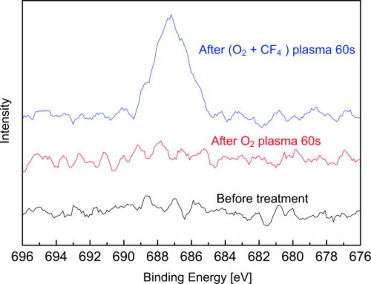
Figure 5. (Color online) Spectra of F 1s from silicon (100) surfaces before and after plasma treatment.
Figure 6 represents spectra of Si 2p before and after different plasma treatments. Si–Si peak is at 98.8 eV in our measurement and no chemical shift is detected with either of plasma treatment. However, Si–O peak (102.6 eV for before treatment) shifts to 103.2 eV after O2 plasma treatment. It is an evidence of silicon oxide formation during plasma treatment. For the sample after (O2 + CF4) plasma treatment, Si–O peak shifts to 103.6 eV and it can be assigned to the formation of O–Si–F on the surface.
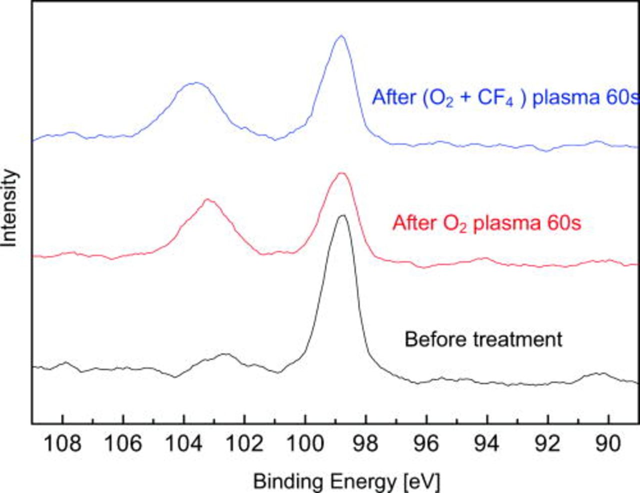
Figure 6. (Color online) Spectra of Si 2p from silicon (100) surfaces before and after plasma treatment.
Figure 7 shows infrared (IR) image of the bonded Si/Si wafer pair at room temperature was prepared by (O2 + CF4) plasma treatment. Since the surfaces keep smooth after plasma treatment, the bonding is uniform over the whole bonded area. Although the wafers were not cleaned by wet chemistry solution prior to bonding, no void is visible in the IR image with the exception of very small peripheral region. It implies most of surface particles and organic contaminants (e.g., hydrocarbons) were removed by the plasma treatment so that very few voids were formed at the interface over the entire bonded pair. Figure 8 shows a cross-sectional HRTEM image of the bonding interface for the Si/Si bonded pair which was prepared by (O2 + CF4) plasma at room temperature without any annealing. Neither microvoid nor gap is observed at the bonding interface. The intermediate layer (bright color between Si/Si) is amorphous state and its two sides is <100> single crystal of bulk Si on the basis of the diffraction pattern. In addition, using energy dispersive x-ray spectroscopy (EDX), we know the amorphous layer contains silicon, oxygen and a small amount of fluorine. Since the bonding interface is intimate without microvoid, it reveals that the surface is still smooth after treated by (O2 + CF4) plasma. This matches well with the results of surface roughness measured by AFM.
Figure 7. IR image of the bonded Si/Si wafer pair at room temperature prepared by (O2 + CF4) plasma treatment. With the exception of small peripheral region, the bonding is uniform over the whole bonded area.
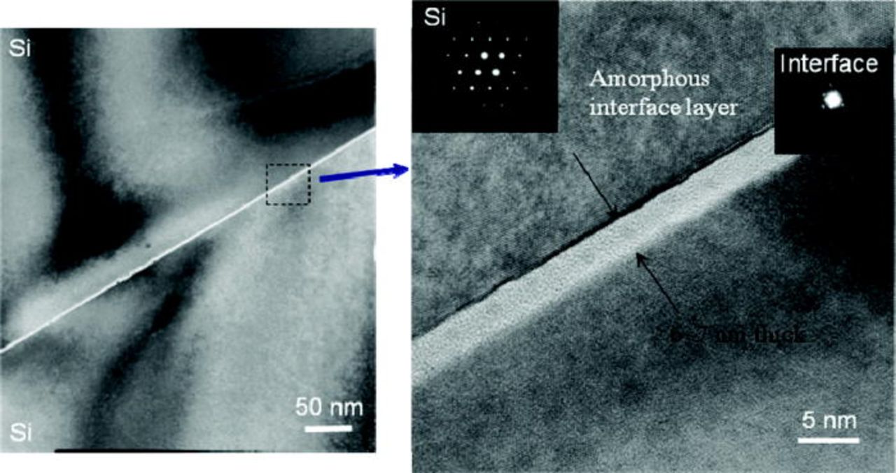
Figure 8. (Color online) Cross-sectional HRTEM images of the Si/Si bonding interface prepared by (O2 + CF4) RIE plasma activation.
Moreover, in order to explore the water molecules at bonding interface, a multiple internal transmission (MIT) IR spectra of Si/Si bonded pairs were measured using single-pass multiple internal-reflection elements. These elements, prepared from infrared transparent material (KRS-5), are pressed gently to the silicon surface to get optical contact and to allow the IR light to enter the silicon and exit from other elements, as shown in Fig. 9. In our experiment, the IR radiation through the Si/Si bonding interface region passes 52 times. The IR spectra were measured using a dry, air-purged Fourier transform infrared spectrometer (FT-IR) in the spectral range of 400–4000 cm−1 with a spectral resolution of 4 cm−1. The transmission spectrum of the empty channel of the spectrometer, without a reflection unit, was used as a reference spectrum. The number of scans was 1024.
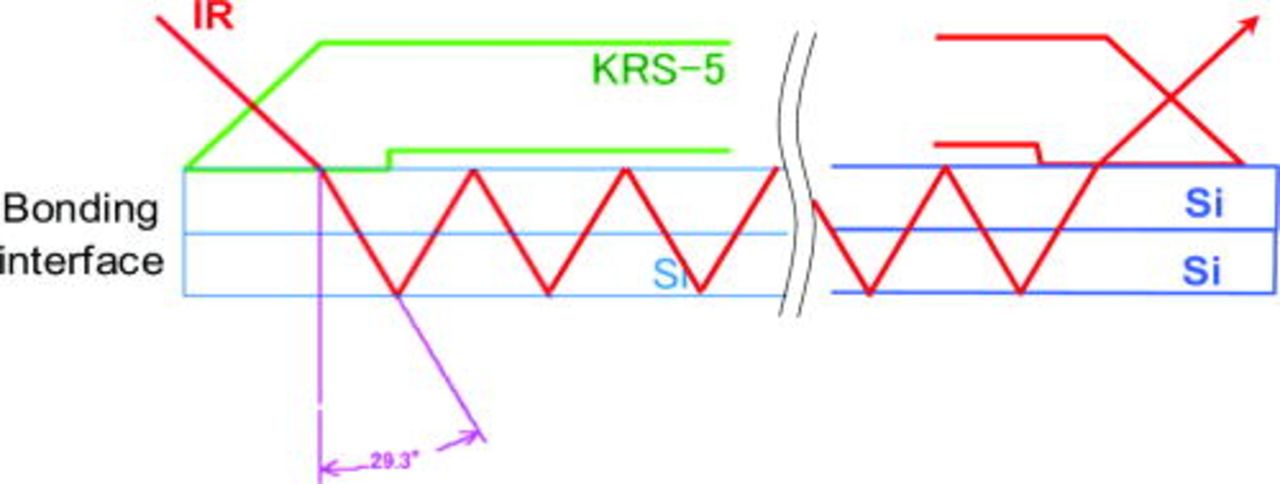
Figure 9. (Color online) Geometry of FT-IR multiple internal transmission (MIT) experiment.
Two Si/Si bonded pairs were prepared by O2 plasma and (O2 + CF4) plasma activation for 60 s respectively. After bonding, both of them are stored in air for 24 h. As shown in Fig. 10, O–H absorption bond was detected at the bonding interfaces of both of samples. The peaks at around 3400–3500 cm−1 correspond to bound H2O by hydrogen bond to silanol groups.12 It suggests that some water molecules are still remaining at the bonding interfaces after 24 h storage. Furthermore, comparing the two spectra, the amount of water molecules remaining at the bonding interface prepared by (O2 + CF4) plasma treatment is fewer than those by O2 plasma treatment.
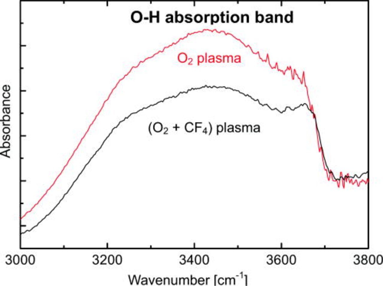
Figure 10. (Color online) FT-IR MIT spectra of the Si/Si bonded wafer pairs prepared by O2 plasma and (O2 + CF4) plasma activation.
Here we discuss the reason why the bonding strength of Si/Si is increased by adding CF4 into O2 plasma. It is reported that occurrence of fluorinated oxide promotes the diffusion of water inward away from the bonding interface.4, 5 Moreover, by adding CF4 to O2 plasma, F radicals from discharged CF4 are so reactive that they react with silicon surface easily resulting in formation of fluorinated silicon oxide. For silicon surface, usually the more fluorine concentration, the less hydrophilic surface is. Thus, adding CF4 into O2 plasma may restrict the amount of water molecules adsorbed on the surface. After the two wafers are brought into contact, a three-dimensional network of water molecules is formed through van der Waals forces and hydrogen bonds across the two surfaces. It has been reported that hydrogen bonds between Si–OH groups on bonded hydrophilic surfaces will convert to Si–O–Si covalent bonds at room temperature as following reaction

Actually the above polymerization reaction is reversible at temperatures <425°C. Because the polymerization of silanol groups [see Reaction 2] is reversible below 425°C, too many water molecules result in slow fracture of Si–O–Si bond easily. Therefore, the bonding strength is usually weak at room temperature. Much water may be adsorbed on highly hydrophilic surface prepared by O2 plasma. Thus, the bonding strength of the samples prepared by O2 plasma is not high owing to fewer numbers of covalent bonds. However, by optimizing CF4 flow in the plasma treatment, the surface become less hydrophilic and appropriate water molecules enable to be absorbed on the fluorinated surface layer. Moreover, 6–7 nm thick amorphous layers (Si, O and F atoms) across the bonding interfaces at room temperature were observed by HRTEM. This implies that the covalent bonds of fluorinated silicon oxide networks are formed after a long storage period at room temperature.
Figure 11 shows the schematic illustration of room-temperature bonding of Si wafers after fluorine containing plasma activation. In Fig. 11a, the (O2 + CF4) plasma treatment removes the organic contaminants and results in fluorinated oxide surface according to the IR image and XPS results. Because the fluorinated oxide layer is less hydrophilic, water molecules adsorbed on the surface is restricted when the surfaces are exposed to moderately humid air (Fig. 11b). After two surfaces are mated together in air, they pull together due to hydrogen bonds between water molecules, as shown in Fig. 11c. During storage in air at room temperature, water molecules across the interface start to rearrange along the bonding interface and diffuse into the fluorinated oxide layers. Many covalent bonds of Si–O–Si are formed at the interface with removal of water molecules in terms of 2, resulting in partial covalent bonding at room temperature (Fig. 11d). Thus, the bonding strength of Si/Si is very strong even at room temperature. On the other hand, too few water molecules also weaken the bonding strength. Owing to the warpage of Si wafers, there are some gaps in order of 10 microns at the edge of the two contacted wafers. If adequate water molecules are adsorbed on the wafer surfaces, the gap can be closed. Considering the results of bonding strength, we notice that the water molecules may also help to close the gap between the contacted wafers. With increasing the amount of CF4 (0–5 sccm) into O2 plasma, fewer water molecules are adsorbed on the surface so that they are more difficult to close the gap. Therefore, the bonding strength deceases significantly with increasing CF4 flow from 1.5 to 5 sccm. This result shows that CF4 flow in plasma activation must be appropriate to get high bonding strength at room temperature.
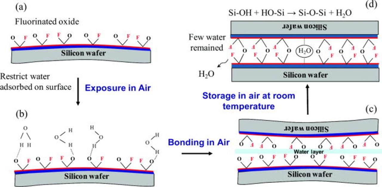
Figure 11. (Color online) Schematic illustration of room-temperature bonding of Si wafers after fluorine containing plasma activation.
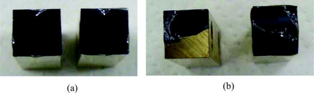
Figure 2. (Color online) Fracture images of room-temperature Si/Si bonding after tensile test. The samples were prepared by (a) O2 plasma and (b) (O2 + CF4 1.25 sccm) plasma.
Conclusion
Room-temperature Si/Si wafer direct bonding without wet chemistry treatment as well as no requiring annealing is developed by simple fluorine containing plasma activated bonding process. In the first part of this paper, the bonding parameters are optimized to improve the bonding strength. Silicon wafers are successfully bonded at room temperature. Compared to the weak bonding strength (∼0.6 J/m2) of Si/Si at room temperature by oxygen plasma activated bonding, very strong bonding strength (∼2.4 J/m2) of Si/Si, close to the bulk-fracture strength of silicon, is achieved optimizing the process parameters of fluorine containing plasma activated bonding.
Moreover, the physical and chemical effects of plasma treatments on wafer surfaces are investigated, respectively. Adding small amount of CF4 into O2 plasma does not etch the Si surface in our experiment, but it results in fluorinated oxide grown on the Si surface. Si/Si bonding interfaces are characterized by HRTEM as well as FT-IR multiple internal transmission to understand the role of water molecules for bonding mechanism. No void is observed at the Si/Si interfaces. We discussed roles of fluorine and water molecules in bonding process. Our results show that the fluorine containing oxygen plasma treatment results in fluorinated oxide on the Si surface, which may control the appropriate water molecules on the wafer. Therefore, many Si–O–Si covalent bonds may be produced in polymerization reaction and contribute to the strong bonding strength at room temperature.
Acknowledgments
We thank Institute for Advanced Micro-system Integration (IMSI) consortium for the financial support of this project. C.W. thanks the Japan Society for the Promotion of Science postdoctoral fellowship for foreign researchers. We are grateful to A. Yamauchi of Bondtech Corporation and G. Kagami of Shinko Seiki Co. Ltd., Japan, for their assistance in bonding experiments.
The University of Tokyo assisted in meeting the publication costs of this article.