
Abstract
In this paper, two approaches combining the separation by implanted oxygen layer transfer (SLT) process with Si epitaxy are proposed to fabricate a silicon-on-insulator (SOI) wafer. Spectroscopic ellipsometry indicates that SOI wafers with the top Si layers of  and
and  are obtained. Defect-free top Si as well as atomic-scale sharp top Si/buried oxide interfaces are observed by transmission electron microscopy, indicating a high crystal quality and a perfect structure of the SLT SOI wafers. Using atomic force microscopy, the surface and top Si/buried oxide interface morphology of the SLT SOI wafers is also investigated.
Export citation and abstract BibTeX RIS
Silicon-on-insulator (SOI) wafers have been widely used in low power/low voltage and high speed ultralarge-scale integrated circuits,1 microelectromechanical systems,2 high voltage power devices,3 and optical waveguides.4 In most of the applications, the bulk silicon quality of the top Si and the thermal oxide properties of the buried oxide (BOX) are required. Currently, bonding and separation by implanted oxygen (SIMOX) are two commercial techniques to produce SOI wafers. Bonding offers SOI wafers with high quality and wide thickness flexibility of both top Si and BOX layers. However, when it comes to thin-film applications, the limitation of bonding SOI arises, such as the inability to produce a top Si layer with good thickness uniformity. In contrast, SIMOX SOI offers a top Si layer with good thickness uniformity; however, it suffers from the limited thickness of the BOX layer. Furthermore, the BOX quality of SIMOX is not as good as that of a thermally oxidized  . It is reported that Si islands5 and pinholes6 in the BOX layer lead to the degradation of breakdown voltage and leakage current, respectively.
The separation by implanted oxygen wafer bonding (SWB) process to fabricate an ultrathin-film SOI was proposed by Tong and Gösele.7 In this process, the top Si layer of a high dose SIMOX donor wafer was transferred onto a thermally oxidized Si handle wafer. The SIMOX donor wafer provides thickness uniformity to the top Si. The thermal growth of the oxide and the wafer bonding provide high quality and good uniformity to the BOX. Therefore, this method combined the advantages of both bonding and SIMOX techniques. However, a high dose oxygen implantation led to the poor crystal quality of the top Si and high cost, which prevented the SWB process from being an industrial application.
Recently, an approach, referred to as separation by implanted oxygen layer transfer (SLT),8, 9 was proposed to fabricate thin-film SOI wafers. Compared to Tong and Gösele's work,7 an ultralow dose SIMOX SOI substrate was used as the starting material for the donor wafer, for the great improvement in the crystal quality of the SIMOX achieved by low dose implantation10 and the internal thermal oxidation11, 12 process. For example, more than  defects are observed in high dose SIMOX, whereas less than
  defects are found in low dose SIMOX. Meanwhile, with the reduced implantation dose, the fabrication cost decreased dramatically. Thus, the SLT process opens up an innovative way of synthesizing SOI wafers for the electronics industry.
In this paper, two approaches involving different SLT/epitaxy sequences are proposed to fabricate SOI wafers: The first approach, denoted as process A, is the formation of the SIMOX donor wafer with the desired thickness of the top Si by Si epitaxy before the SLT process, and the second approach, denoted as process B, is the formation of the thin-film SOI seed wafer by SLT process before Si epitaxy. The authors investigate the cross-sectional structure of the SLT SOI wafers by transmission electron microscopy (TEM). The surface morphology of the SOI wafers is analyzed by atomic force microscopy (AFM), and methods for improving their surface roughness are proposed. Finally, comparisons of the top Si/BOX interface morphology and wafer edge exclusion area of the two samples are also discussed.
Experimental
Fabrication of SIMOX donor wafers
Ultralow dose  ranging from
  to
to  was implanted into 150 mm p-type (100) Czochralski Si wafers at 150–200 keV. The wafer temperature was kept at
  during implantation. Subsequently, the as-implanted wafers were annealed at
  in a mixed atmosphere (5% oxygen and 95% argon) for 8 h. The SIMOX donor wafers with a 190 nm thick top Si and a 120 nm thick BOX were obtained after annealing.
Fabrication of sample A by process A
The process flow is shown in Fig. 1a. First, a  thick epitaxial Si layer was deposited onto the SIMOX donor wafer by chemical vapor deposition. The SIMOX donor wafer was then oxidized in a wet oxygen atmosphere at
  . Both the as-oxidized SIMOX donor wafers and the Si handle wafers were cleaned in modified solutions of
  (SC-1) and
  (SC-2), followed by rinsing in deionized water and spin drying. Afterward, the SIMOX donor wafer was bonded upside down to the Si handle wafer at room temperature. The interface strengthen annealing for the bonded wafer pair was performed at
  in wet oxygen for 3 h. The annealed wafer pair was grinded from the back side of the SIMOX donor wafer until a
  Si layer was left. A 5% tetramethylammonium hydroxide (TMAH) solution was used to remove the remaining Si layer of the donor wafer at
  up to the
  , and then the etch-stop layer was removed with 5% HF solution. Finally, the SOI wafer with a
  top Si layer on top of a
  BOX layer was obtained.
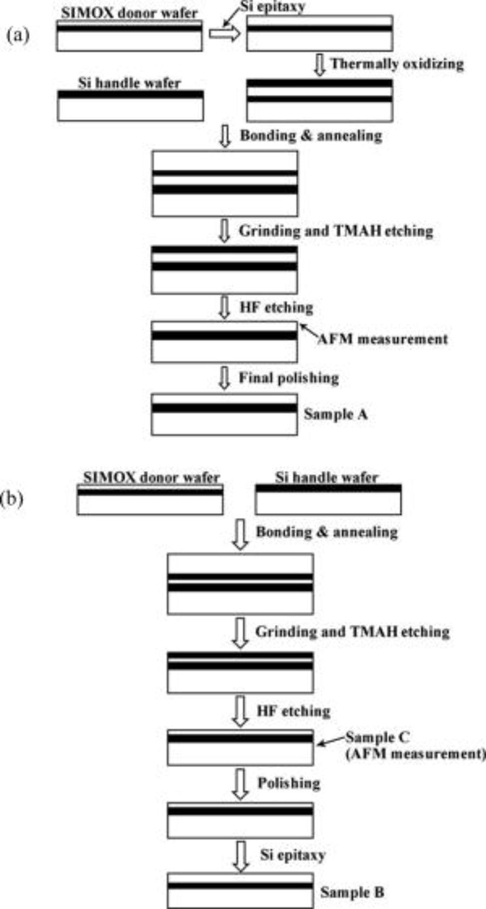
Figure 1. Schematic diagram of the fabrication flow of (a) process A and (b) process B.
Fabrication of sample B by process B
As shown in Fig. 1b, process B can be divided into two steps. First, a 150 mm thin-film SLT SOI seed wafer denoted as sample C was obtained by transferring the top Si of the SIMOX donor wafer upside down onto a thermally oxidized Si handle wafer.8 Second, after cleaning and spin drying, the Si epitaxial layer was grown on sample C with a similar epitaxial process used in process A. Finally, SOI wafer with a  top Si and a
  BOX layer was fabricated.
Results and Discussion
Characterization of the top Si thickness uniformity and cross-sectional structure of the SOI wafers
The key issue in fabricating SOI wafers is to achieve a top Si with good thickness uniformity, which guarantees uniform device characteristics. To evaluate the thickness uniformity of the top Si, samples A and B with 4 mm edge exclusions were measured by spectroscopic ellipsometry (SE) at 49 locations over the entire wafer. The top Si thickness distributions of samples A and B are shown in Fig. 2. As shown in curve A, the average top Si thickness of sample A is 1491.46 nm and the thickness variation is ±14.9 nm, while those of sample B, as shown in curve B, are 1476.44 nm and ±18.5 nm, respectively. Clearly, top Si layers with excellent thickness uniformity can be achieved by both processes A and B, and the top Si thickness variations in samples A and B are comparable.
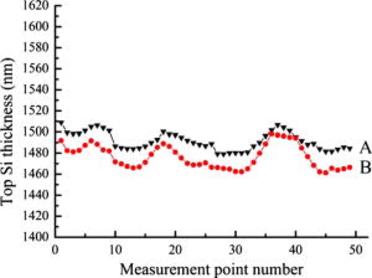
Figure 2. Top Si thickness of the SLT SOI wafers.
To investigate the microstructure of the SLT SOI wafers, TEM is performed. The cross-sectional transmission electron microscopy (XTEM) images of samples A and B are shown in Fig. 3a and 3b. Clearly, a sandwichlike structure including the top Si, the BOX, and the Si substrate can be distinguished, and the sharp and straight interfaces can be observed. The results reveal the perfect structure of samples A and B. High resolution TEM images of the interfacial region between the top Si and the BOX of samples A and B are shown in Fig. 4a and 4b. Atomic-scale sharp interfaces without undulation are clearly demonstrated. No discernible defects can be observed, indicating a high crystal quality of the top Si.
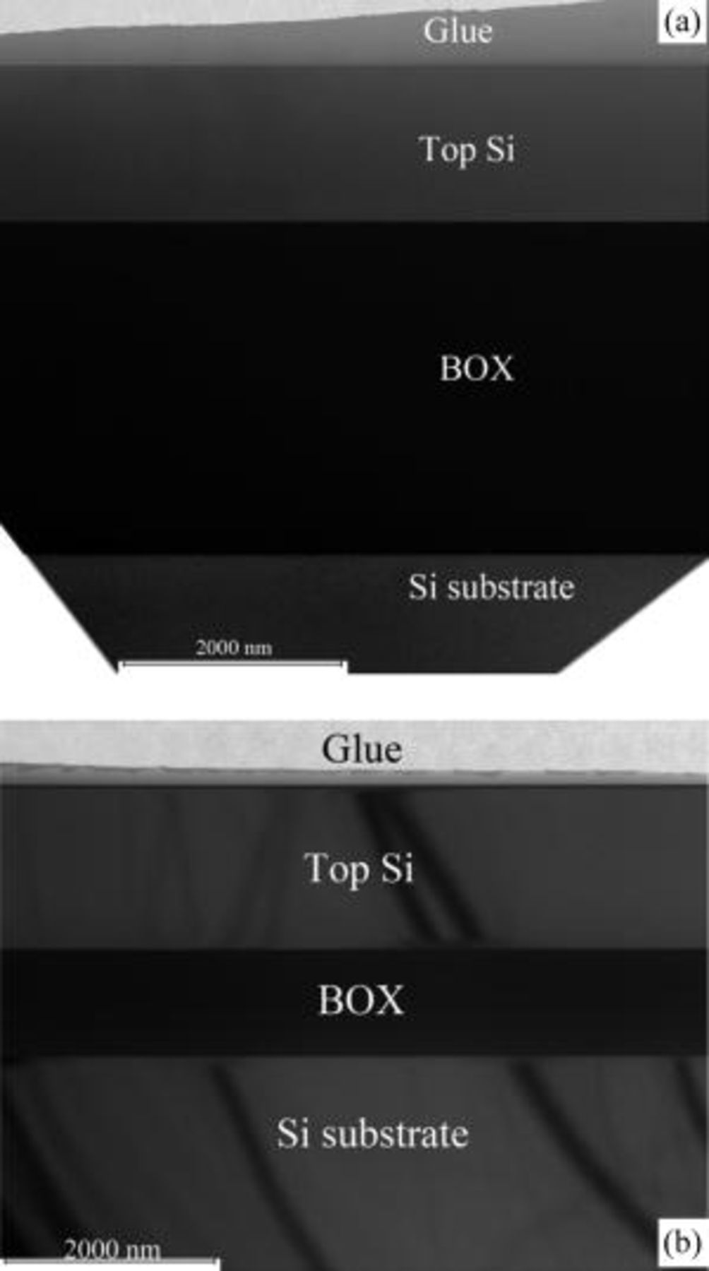
Figure 3. XTEM image of (a) sample A and (b) sample B.
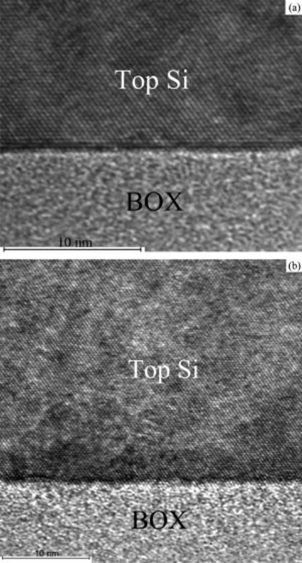
Figure 4. High resolution TEM image of the top Si/BOX interfacial region of (a) sample A and (b) sample B.
Surface morphology of the SOI wafers
The surface roughness of SOI wafers has important implications for processing and device performance, especially for gate oxide integrity and reliability. It has been reported that the gate oxide of an SOI metal-oxide-semiconductor field-effect transistor has a higher incidence of suffering a low voltage breakdown than that on bulk wafers. This effect is due to the increased surface roughness of SOI wafers, which leads to a higher thermal oxide defect density than that of the bulk wafers.13
As shown in Fig. 1a and 1b, the surface roughness of samples A and C was measured by AFM just after removing the BOX of the SIMOX donor wafer. The average root-mean-square (rms) surface roughness (calculated from a  scan area) is 2.383 and 2.944 nm, respectively. Importantly, these values are much smaller than that of hydrogen-implantation-split SOI wafers
  ,14, 15 which bring more convenience in the following chemical mechanical polishing (CMP) process. As shown in Fig. 5a and 5b, square pits are observed on the surfaces of both samples A and C. The size and depth of the pits are less than
  and 10 nm, respectively. This configuration is believed to reflect the crystal orientation of the top Si, and the edges of the square pits are along the [110] crystal orientation. Such square pit morphology can be explained by the top Si/BOX interface morphology of the SIMOX donor wafer. As reported by Guilhalmenc et al.16 and Ishiyama and Omura,17 the convex square mosaics with the sides of [110] crystal orientation, as shown in Fig. 6, were formed on the upper interface of the SIMOX BOX due to the recrystallization of the damaged silicon layer and the orientation-dependent oxidation occurring during the SIMOX BOX formation. In the SLT process, the top Si of the SIMOX donor wafer is transferred upside down onto the Si handle wafer. As a result, there are square pits with [110] direction edges left on the surface of the SLT SOI after removing the SIMOX BOX. Besides, we cannot rule out the effect of nonuniform etching due to
  transition regions with different local stoichiometries existing near the top Si/BOX interface of SIMOX. It mainly increases the depth of the square pits and makes their shape irregular. Moreover, the surface morphology of the SLT SOI can be greatly improved by optimizing the annealing process of SIMOX because the convex square mosaics can be eliminated after a sufficient period of annealing.17 Compared to the annealing process of fabricating the SIMOX donor wafer, an additional 4 h annealing was added. The surface morphology of the SLT SOI fabricated with the modified process is shown in Fig. 7. The rms surface roughness is 1.097 nm and the depth of the square pits is less than 5 nm. The results demonstrate a remarkable improvement in the surface roughness than in both Fig. 5a and 5b.
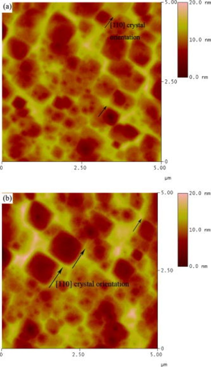
Figure 5. AFM image of the surface morphology of (a) sample A and (b) sample C.
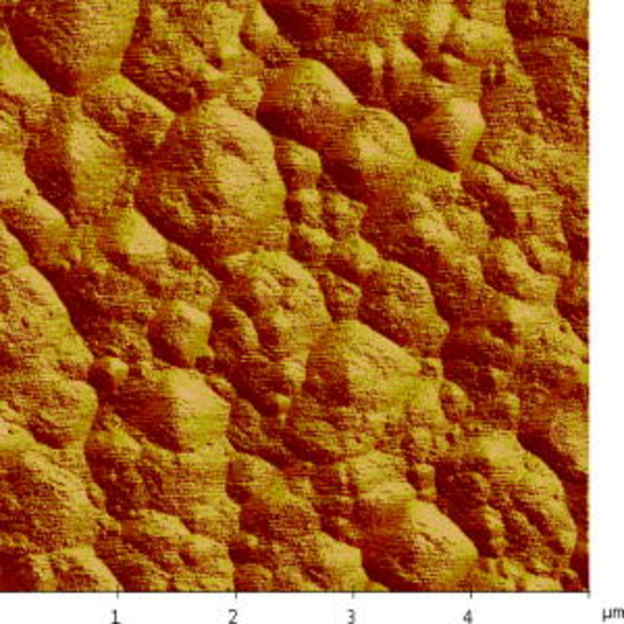
Figure 6. Top-view AFM image of the upper BOX interface of the SIMOX donor wafer.
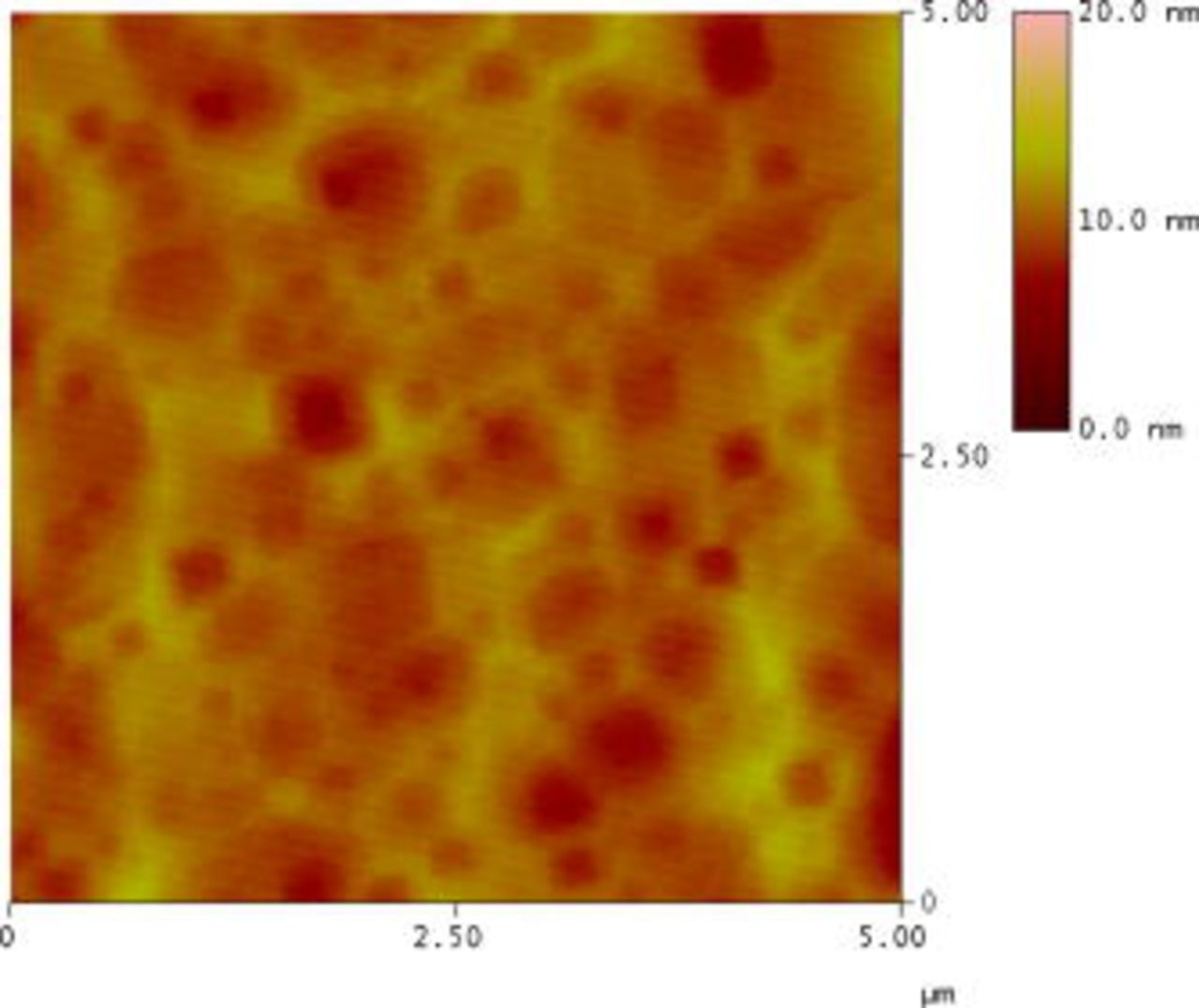
Figure 7. Surface morphology of the SLT SOI obtained after optimizing the annealing process of the SIMOX donor wafer.
To further improve the surface roughness, CMP is needed. The crystal quality of the top Si layer also benefits from CMP because the material removed by CMP originated from the top Si/BOX interfacial region, which contains numerous embedded defects.18
Top Si/BOX interface morphology and wafer edge exclusion area of the SOI wafers
For the top Si/BOX interface morphology characterization, the top Si layers of both samples A and B were etched by a 5% TMAH solution heated to  until the upper surface of the BOX layers was exposed. The interface morphology of samples A and B is shown in Fig. 8a and 8b, and their rms surface roughness is 0.138 and 1.152 nm, respectively. The difference between samples A and B in interface morphology can be explained by the different fabrication process. For sample A, the BOX was formed through a standard thermal oxidation of the SIMOX donor wafer after Si epitaxy, and the thermal growth of
  offers an atomically flat
  interface. For sample B, the top Si/BOX interface originated from the surface thermal oxide/top Si interface of the SIMOX donor wafer because the surface thermal oxide layer was kept to enhance the bondability of the SIMOX donor wafer.8 The rough surface thermal oxide/top Si interface of the SIMOX donor wafer can be attributed to the bombardment of the oxygen ion implantation as well as the recrystallization of the damaged silicon layer. The interface quality of the top Si/BOX layers significantly influences the performance of devices especially for fully depleted complementary metal oxide semiconductor (CMOS) devices built on SOI wafers. For instance, the rough interface scatters the electrons and further results in electron mobility and lifetime degradation. Thus, from this point of view, process A is also superior to process B.
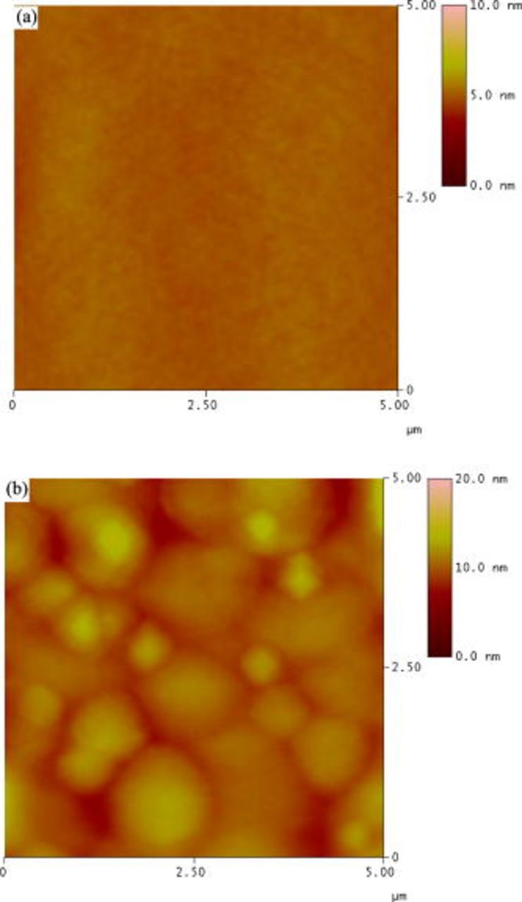
Figure 8. AFM image of the upper BOX surface of (a) sample A and (b) sample B after the removal of the top Si layers.
Compared to sample A, a grain band is observed at the wafer edge exclusion area of sample B. Clearly, the grains with different facets are shown in Fig. 9. The component of the grains is analyzed by electron dispersive spectroscopy. The result indicates that the grains consists of Si. In consideration of the fabrication process, the Si grains result from the Si epitaxy. In process B, a 4 mm exclusion area was formed at the wafer periphery of sample C after the layer transfer, i.e., some oxide residues coming from the BOX layer were exposed at the site. Thus, the polycrystalline Si grains were formed at the wafer edge exclusion area by depositing Si directly onto the amorphous residual oxide during the epitaxy process. Because the polycrystalline silicon grains cause particle issue in the following CMOS process, process A is preferred for use in industrial production.
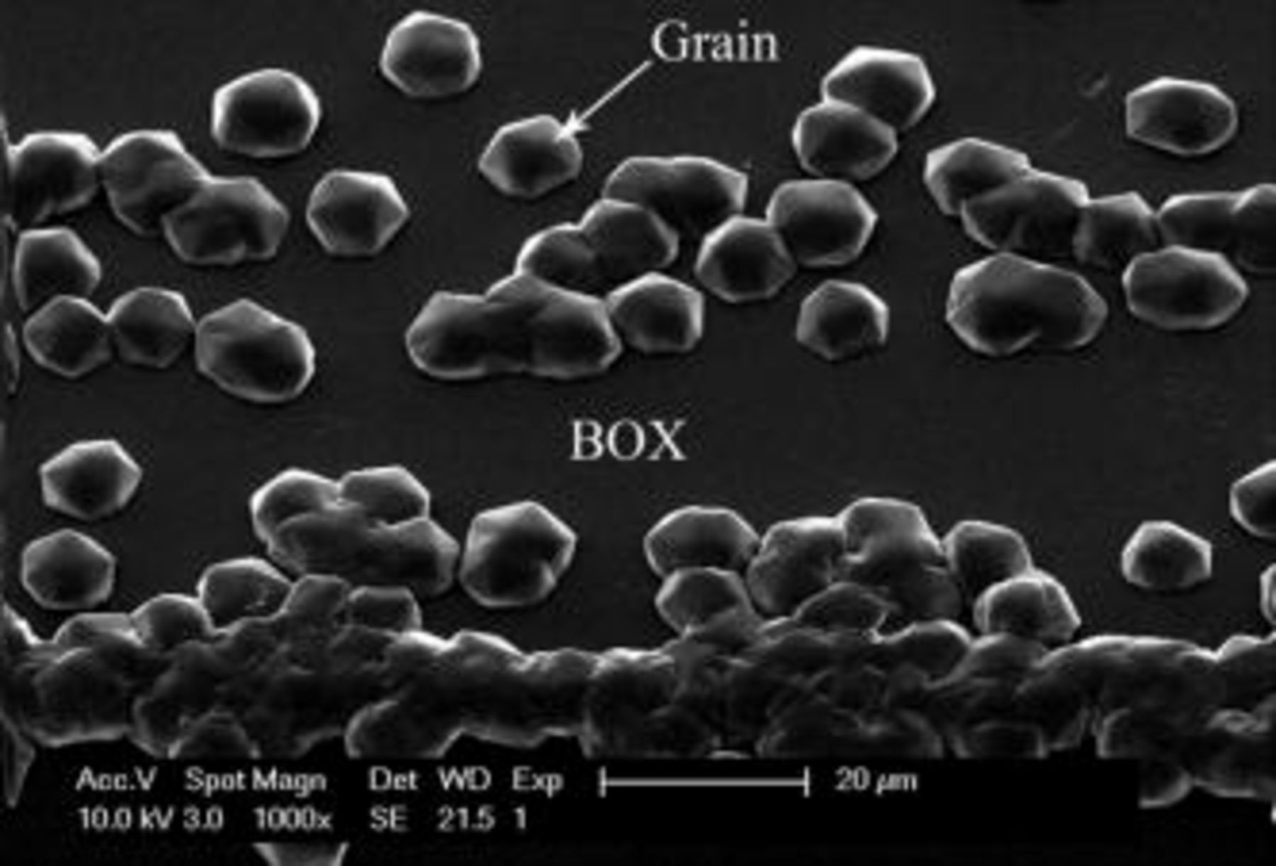
Figure 9. SEM image of the Si grains at the wafer edge exclusion area of sample B.
Conclusions
To fabricate high quality SOI wafers, two approaches involving different SLT/epitaxy sequences are investigated. SE results indicate that the top layers with excellent thickness uniformity are achieved successfully by both processes A and B. The results of TEM show sharp interfaces and defect-free top Si layers, revealing the perfect structure of the SLT SOI wafers. For sample B, a rougher top Si/BOX interface and a grain band at the wafer periphery are observed, which further degrade device characteristics and cause particle issue in the following CMOS process, respectively. Therefore, process A is a more competitive approach for fabricating high quality SOI wafers.
Acknowledgments
This work was financially supported by the National Science and Technology Major Projects (grant no. 2009ZX02040), the National Basic Research Program of China (973 Program, grant no. 2010CB832906), the National Science Foundation of China (grant no. 60721004), and the Shanghai Institute of Microsystem and Information Technology Fund for Young Scholars.
Shanghai Institute of Microsystem and Information Technology, assisted in meeting the publication costs of this article.