
Abstract
This study aims to investigate the interaction forces between silica particles and wafer surfaces during chemical mechanical planarization of copper. Silica slurry is most commonly used in the final step of Cu polishing to reduce scratches, Cu dishing, and oxide erosion. This study measures and calculates the interaction forces between silica particles and tetraethylorthosilicate oxide, TaN, Cu, and low-dielectric constant material surfaces. The Derjaguin-Landau-Verwey-Overbeek theory was used to calculate these forces by measuring the zeta potentials of the particles and the surfaces. The interaction force was obtained directly by measuring the force on the particles as a function of the distance between the particle and the surface. An atomic force microscope was used. Likewise, the magnitude of particle contamination on the wafers was measured by field-emission scanning electron microscope after the wafers were polished. The weakest repulsion force was measured between silica particles and the TaN surface. Similarly, the highest number of particles was observed on TaN surfaces after they were polished. © 2003 The Electrochemical Society. All rights reserved.
Export citation and abstract BibTeX RIS
Due to the low resistivity and high electromigration performance of Cu, it is considered a much better interconnection material than the currently used Al-based alloys.1 However, while there is a clear advantage in using Cu as an alternative material to Al, there are several challenges that must be overcome.
One such challenge is the difficulty involved in the patterning of Cu by dry etching. The damascene technology using chemical mechanical planarization (CMP) is the only technology that can provide global planar surfaces and patterned Cu interconnection with a large process window.2
The other problem of Cu CMP is Cu contamination during device manufacture. Cu is considered a very serious metallic contaminant for silicon devices. The detrimental effects of Cu contamination of the intermetal and interlevel dielectric are well known.3
Compared to other materials such as oxide and W, Cu is a softer material and tends to cause more scratches and dishing during CMP. Thus, Cu CMP involves two polishing steps. In the first step, acidic-pH alumina or silica slurry is used for faster removal of Cu until the TaN barrier surface is exposed. In the second step, alkaline silica slurry is commonly used to bring the ratio of the polishing selectivity of Cu to the barrier layer (TaN) to the dielectric TEOS (tetraethylorthosilicate) oxide or low dielectric constant materials) close to 1:1:1.
After the second polishing step, the Cu, TaN, and dielectric materials are exposed to silica slurry particles. The interaction of silica particles with these polished surfaces will determine the polishing behavior and the level of particle contamination after Cu CMP.
In this paper, the interaction forces between particles and surfaces during Cu CMP were calculated based on the Derjaguin-Landau-Verwey-Overbeek (DLVO) theory4 5 for different pH ranges. The adhesion forces between the particles and surfaces were also experimentally measured using an atomic force microscope (AFM). Likewise, the magnitudes of particle contamination on TEOS oxide and low-dielectric constant polymer, Cu, and TaN surfaces were observed after they were polished to confirm the resulting interaction forces.
Experimental
For this experiment, TEOS oxide, SiLK™ (Dow Chemical Co.), TaN, and Cu deposited wafers were used as substrates. Table I shows in detail the materials used in the experiment. The formulations of SiLK were presumed to consist essentially of a mixture of monomeric or oligomeric aromatic starting compounds, which contain the ortho-bis-ethynyl or ortho-phenylethinyl group.6 Figure 1 shows the schematic structure of polymerized SiLK.
Table I.
| Films and particles used in the experiment. | ||
|---|---|---|
| Films | TEOS | 1200 Å, CVD |
| Cu | 1 μm, sputtering | |
| TaN | 600 Å, sputtering | |
| SiLK | 400 Å, spin coating | |
| Particles | Colloidal silica | 100 nm (Sigma-Aldrich Co.) |
| Glass particle | 20 μm (Duke Scientific Co.) | |

Figure 1. Schematic chemical structure of polymerized SiLK.5
The TEOS deposited wafer was cleaned in a mixture of  and
and  (4:1 in vol %), and then treated with dilute hydrofluoric acid (DHF) to remove organic contaminants. The SiLK, TaN, and Cu deposited wafers were precleaned in an isopolyacid (IPA) solution and then rinsed with DI water to remove organic contaminants. The semiconductor-grade wet chemicals used in the experiment were provided by Dong Woo Fine Chemical Company.
The zeta potentials of all materials used in this study were measured as a function of pH, using a LEZA-600 (Otsuka Electronics, Co.) zeta potential analyzer.
The interaction force was measured using an AFM (AutoProbe® CP Research, Park Scientific Co.) by analyzing the force on the cantilever as a function of the distance between the cantilever and the surfaces in a  KCl solution at different pH values. A liquid cell was used. For the interaction force measurements, a glass particle with a radius of 20 μm (Duke Scientific Co.) was attached to a tipless cantilever of AFM. Figure 2 shows the optical micrograph of a silica particle on a tipless cantilever.

Figure 2. The optical micrograph of a silica particle on a tipless cantilever.
The wafers were polished with colloidal silica slurry on a polisher (PM5 polisher, Logitech Co.). The rotation speeds of the head and platen were set at 30 rpm. The pressure of the carrier was 3 psi, and the polishing time was set at 1 min. The slurry flow rate was 120 mL/min. For the preparation of the slurry, a shaker, and ultrasonic power were applied for 60 and 30 min., respectively. The slurry for Cu CMP was prepared by mixing 6 wt % colloidal silica particles and a corrosion inhibitor (Bezotriazol, BTA,  in a
in a  KCl solution (the same chemical composition as that of the solution for the AFM measurements). The polished wafer surfaces were observed using field-emission scanning electron microscopy (JSM-6330F, JEOL Co.) to measure the level of particle contamination on the surfaces. All pHs were adjusted by HCI and NaOH.
Results and Discussions
The zeta potentials of the slurry particles and wafers were measured as shown in Fig. 3. Colloidal silica particles showed very stable suspension in the pH ranges investigated. No changes in particle size were observed. Due to the high conductivity of the Cu surface, Cu particles instead of Cu wafers were used to measure the zeta potential. All surfaces showed negative zeta potentials in the pH range investigated. Likewise, the TaN surface showed the least changes in zeta potential as a function of solution pH. The lowest zeta potentials were measured on the TEOS oxide surfaces.

Figure 3. The zeta potential of (a) colloidal silica particles, (b) SiLK, TEOS, Cu, and TaN wafers as a function of solution pH.
The DLVO theory4
5 estimates the repulsive and attractive forces resulting from the overlap of electric double layers and the London-van der Waals force, as a function of interparticle distance. The total interaction  occurring between the particles and the wafer surface in the solution is the sum of van der Waals force
  and the electrostatic force
  as shown in Eq. 1 below

If a small interparticle surface separation (H) is assumed, the van der Waals force between a sphere and a substrate can be expressed as

where  is the Hamaker constant for surfaces 1 and 2 in a dispersion medium 3, calculated based on an
  value, and R is the radius of a sphere. The Hamaker constant of TaN was calculated based on its definition,7 as shown below

where n is the number of atoms per unit volume,  is
is 
 is the ionization potential, and α is the polarizability. For low-dielectric constant organic materials, typical values for organic materials were used for the calculation. The Hamaker constants used for this study are summarized in Table II.
Table II.
| Hamaker constants used for van der Waals force calculation. | |
|---|---|
| Materials |
 |
| Water | 4.38 (Ref. 10) |
 | 50 (Ref. 10) |
| Cu | 28.4 (Ref. 11) |
| TaN | 25.9a |
| Organic materials | 2-10 (Ref. 12) |
| a Based on Eq. 3 | |
The calculation of the electrostatic force is more complex due to the overlapping of the diffused double layers between two surfaces. It must rely on numerical solutions or various approximations. Overbeek's approximation8 9 10 was used for the calculation of the electrostatic force due to larger than ±25 mV zeta potentials on surfaces, as shown below:

where

ɛ is the permittivity of the dispersion medium, k is the Boltzmann constant, and T is the temperature. z is the counter ion charge number, R is the particle radius, and the debye length 1/κ is  while
while  is the zeta potential of the surfaces.
Figure 4 shows the DLVO total interaction force between a silica particle and wafer surfaces as a function of the distance between them. A stronger attractive force was calculated for silica particles on wafers in acidic rather than in alkaline solutions. In the alkaline and neutral pH ranges investigated, the strongest attractive interaction force was calculated between colloidal silica particles and the TaN wafer. In the acidic solution, silica particles showed the strongest attractive forces with the Cu, TaN, and TEOS wafers. On the other hand, the weakest attractive interaction force was calculated between silica particles and the SiLK surface in all pH ranges. This was probably due to the small Hamaker constant value of SiLK that was applied for the calculation of the interaction force.

Figure 4. DLVO total interaction force between silica particle and various wafer surfaces at solution of (a) pH 11, (b) 7, and (c) 3.
The change in the interaction force between the particle and a surface can be measured with an AFM as the cantilever approaches the substrate.11 The AFM probes the surface of a sample with a sharp tip that is several micrometers long and often less than 100 Å in diameter. The tip is located at the free end of a cantilever. Forces between the tip and the sample surface cause the cantilever to bend or deflect. A detector measures the cantilever deflection as the tip scans the surface of the sample.
Several forces typically contribute to the deflection of an AFM cantilever. The force most commonly associated with an AFM in air is an interatomic force called the van der Waals force. Figure 5 shows a typical force vs. distance curve or force curve, which was used in the experiments. Force curves show the deflection of the free end of the AFM cantilever as the fixed end of the cantilever is brought vertically towards and then away from the sample surface. Figure 5a shows the typical hysteresis force curve as a function of the distance between the surface and the tip. Figure 5b is a schematic diagram of cantilever shapes at each point of the force curve, as the cantilever moves.

Figure 5. The change of (a) force curves and (b) cantilever shapes as a function of the distance between the tip and surface.
As the cantilever tip is brought very close to the surface, it may jump into contact with the surface, if it feels a sufficient attractive force from the sample indicated [Fig. 5b(2)]. Once the tip is in contact with the surface, the cantilever deflection will increase as the fixed end of the cantilever is brought closer to the sample [Fig. 5b(3)]. After loading the cantilever to a desired force value, the process is reversed. A key measurement of the AFM force curve is shown in Fig. 5b(5). At this point, the adhesion is broken, and the cantilever is freed from the surface. This can be used to measure the adhesion force between the tip and the surfaces. The bigger jump-out point causes greater attractive interaction force.12
Figure 6 shows the measured interaction forces between the particles and surfaces at the point of in Fig. 5b(5). The attractive forces of silica particles on SiLK, TEOS, Cu, and TaN surfaces in alkaline solutions were measured to be 0.23, −0.78, −2.02, and −2.04 nN, respectively. The strongest attractive force was measured on the TaN surface, while the weakest attractive force was on the SiLK surface. In the neutral solutions, the attractive forces on the SiLK, TEOS, Cu, and TaN wafers were measured to be −0.51, −4.98, −14.46, and −15.11 nN, respectively. In the acidic solutions, the attractive forces of the SiLK, TEOS, Cu, and TaN wafers were measured to be −6.05, −10.11, −18.78, and −20.18 nN, respectively. The SiLK, TEOS, Cu, and TaN wafers were more attractive in acidic solutions than in other solutions. Figure 6 summarizes the interaction forces of silica particles on wafers in solutions of different pH values.

Figure 6. Measured interaction forces between the silica particle and SiLK, TEOS, Cu, and TaN wafer surfaces measured in acidic, neutral, and alkaline solutions.
In all pHs investigated, the measured interaction forces showed trends that were very similar to the calculated ones. A stronger adhesion of particles on surfaces was measured in acidic than in alkaline solutions. TaN surfaces showed the strongest adhesion of silica particles in all pH ranges. On the other hand, the lowest adhesion force of the particles was measured on the low-k polymer, SiLK. The contact angle of SiLK was measured to be −70°, which is hydrophobic. The van der Waals force is usually lower for organic surfaces, due to the latter's low Hamaker constant values. Hydrophobicity and the low value of the Hamaker constant were considered to be the reasons for the lowest adhesion force, which was between silica particles and the SiLK surface.
In order to confirm the calculated and measured interaction forces, the SiLK, TEOS, Cu and TaN wafers were polished using colloidal silica slurry. FESEM was used to observe the magnitude of particles left on each surface. No particles were observed on the SiLK surface in all pHs (Fig. 7). Figure 8 shows the FESEM images of colloidal silica particles on the TEOS oxide surface. A slight increase in the number of particles was observed on the TEOS surfaces, regardless of the pH of the slurries. On the other hand, Fig. 9 shows the FESEM images of colloidal silica particles on Cu surfaces when they were polished in alkaline, neutral, and acidic slurries. Fewer particles were found on the Cu wafer when the latter was polished in alkaline, than in the acidic slurry.

Figure 7. FESEM images of particles on SiLK wafer after polishing in silica slurry of (a) pH 11, (b) pH 7, and (c) pH 3.
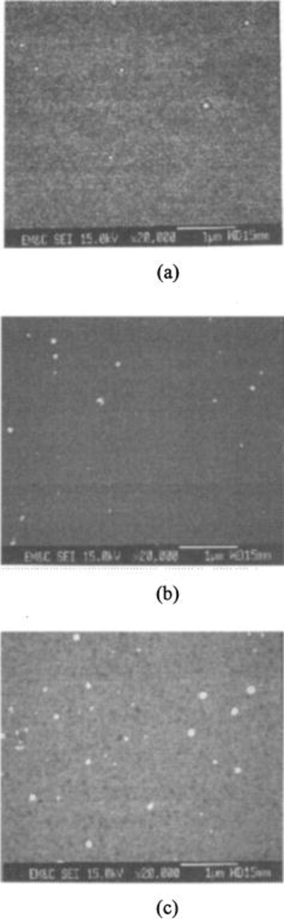
Figure 8. FESEM images of particles on TEOS wafer after polishing in silica slurry of (a) pH 11, (b) pH 7, and (c) pH 3.
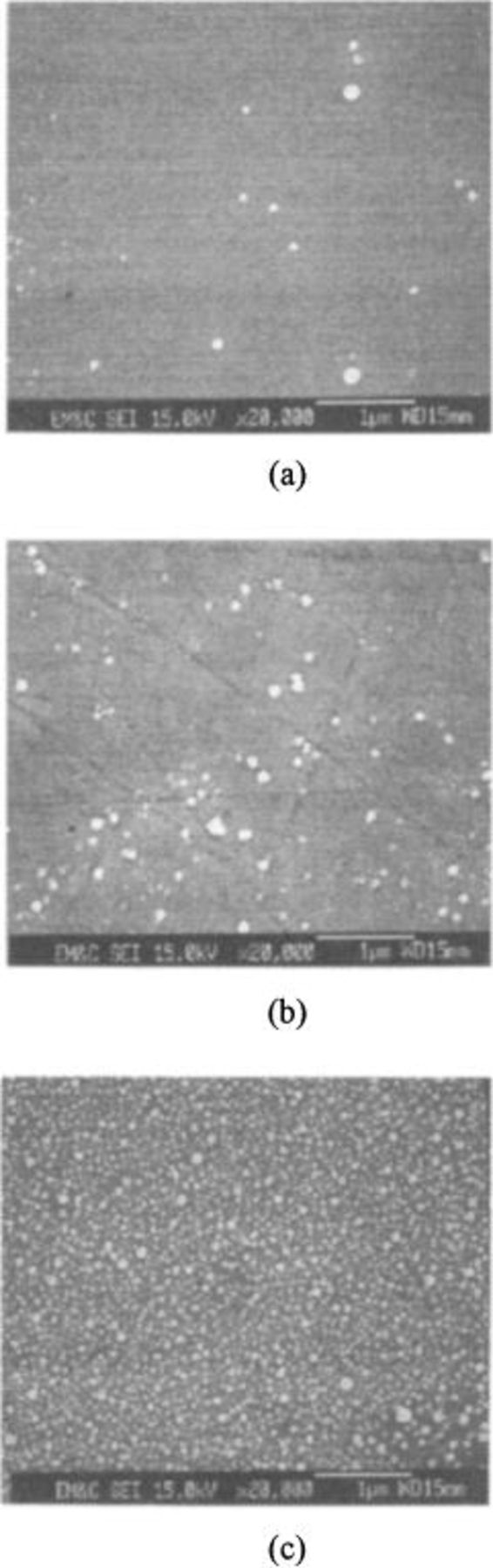
Figure 9. FESEM images of particles on Cu wafer after polishing in silica slurry of (a) pH 11, (b) pH 7, and (c) pH 3.
Figure 10 shows the FESEM images of colloidal silica particles on TaN surfaces. The greatest numbers of particles were also found on the surface polished in acidic slurry. It could be concluded that TaN and Cu surfaces are very susceptible to particle contamination in acidic slurry during Cu polishing.

Figure 10. FESEM images of particles on TaN wafer after polishing in silica slurry of (a) pH 11, (b) pH 7, and (c) pH 3.
Conclusions
The zeta potentials of slurry particles and wafer surfaces were measured to calculate the total interaction force between the particles and substrates based on the DLVO theory. More attractive forces were calculated between colloidal silica particles and wafer surfaces in acidic rather than in alkaline slurry. The adhesion force between colloidal silica particles on the cantilever and the wafers was measured using an AFM. Colloidal silica particles showed the strongest adhesion on the TaN surface and the weakest adhesion on the SiLK surface. Experimental measurement of interaction forces supported the theoretical calculation of interaction forces between colloidal silica particles and wafer surfaces. In order to compare these results, particles on substrates were observed by FESEM after the surfaces were polished with colloidal silica slurries. The smallest and largest number of particles were observed on the SiLK wafer, and the TaN wafer, respectively. The pH of the slurry and the zeta potentials of the surfaces played important roles in controlling the interaction forces of colloidal silica particles on polished surfaces. Alkaline slurry was much more desirable in controlling the level of particle contamination during Cu CMP.
Acknowledgments
This work was supported by Dongwoo Fine Chemical Company. S.Y.L's scholarship was by courtesy of Hanyang University.
Hangang University assisted in meeting the publication costs of this article.