Abstract
Cyclic voltammetry and chronoamperometry were used to study the deposition process at the initial stage of Cu2O electrodeposition on indium tin oxide-coated glass. The current transient data and predicted values were analyzed by the instantaneous and progressive nucleation models under different electrolyte concentrations. The effects of the Cu2O nucleation mechanism on microstructure and photoelectric properties of Cu2O were investigated by X-ray photoelectron spectroscopy, X-ray diffractometry, scanning electron microscopy, ultraviolet visible spectrophotometry and fluorescence spectrophotometry. The results show that the electrochemical deposition process of Cu2O is irreversible and controlled by diffusion, and the diffusion coefficient was calculated to be 2.2 × 10⁻⁶ cm2·s−1. The nucleation mechanism of Cu2O is related to the electrolyte concentration. When the concentrations of Cu(AC)2 were 5 mM and 15 mM, the nucleation processes of Cu2O were consistent with the progressive nucleation and instantaneous nucleation models, respectively. Under the instantaneous nucleation mechanism, the prepared Cu2O displayed a uniform structure, composed of sword-shaped dendritic crystal. Compared to the progressive nucleation, the purity of the Cu2O was higher, the bandgap narrower (2.006 eV), and the photoluminescence intensity higher. The Cu2O had a high carrier density (4.9 × 1022 cm−3) and a low charge transfer resistance (127.27 KΩ·cm2). It exhibits superior photoelectric performance.
Export citation and abstract BibTeX RIS

This is an open access article distributed under the terms of the Creative Commons Attribution 4.0 License (CC BY, http://creativecommons.org/licenses/by/4.0/), which permits unrestricted reuse of the work in any medium, provided the original work is properly cited.
The forbidden bandgap of cuprous oxide (Cu2O) is 1.9--2.5 eV. Due to its advantages in abundance, low cost, and nontoxicity, it satisfies the necessary economy and environmental requirements to be a viable material for solar energy conversion. In addition, the position of the conduction band (more negative than −0.7 V vs RHE) provides a large driving force for proton reduction in photoelectric cells.1--3 Therefore, Cu2O can be used in solar cells of high open-circuit voltage in the conventional solid-state configuration.4 Cu2O also has wide applications in memory resistors,5 gas sensors6,7 and catalysts.8,9 Cu2O thin films have been prepared by various techniques such as thermal oxidation,10 electrodeposition,11--13 radio frequency magnetron sputtering,14,15 and atomic layer deposition.16 Among these techniques, electrodeposition has the attractive features of low processing temperature and low instrumentation cost, making it the most common method for the fabrication of Cu2O thin films.
Since the photoelectric conversion efficiency of Cu2O can reach 20% in theory, many scholars have explored the possibility of its application in photovoltaic conversion. However, the current highest photoelectric conversion efficiency is only 5.38%,17,18 due to the high recombination rate of photoproduction electron holes. Due to its electronic structure, the bonding, surface energy, and chemical reactivity of Cu2O have a direct relationship with its surface morphology and grain sizes.19,20 Controlling the Cu2O surface morphology and particle sizes allows one to decrease the Cu2O photoproduction electron-hole recombination rate and thus improve its photoelectric properties. In the electrochemical deposition process, the deposition potential,21 solution composition,22,23 and pH24 influence the surface morphology and particle sizes of Cu2O. Many researchers have focused on varying the electrochemical deposition parameters to control the surface morphology and particle sizes of Cu2O. Fewer have studies the Cu2O nucleation and growth mechanisms and their effect on performance. Nonetheless, the nucleation and growth mechanisms are fundamental factors. Therefore, it is necessary to explore these mechanisms in order to improve the photoelectric efficiency of Cu2O.
This paper studies the Cu2O electrodeposition process from the angle of the driving force through cyclic voltammetric and timing current curves, in order to understand the nucleation mechanism of Cu2O. This will help in designing Cu2O thin film materials. The results will provide more guidance and predictability in the synthesis of materials, so as to improve the photoelectric properties of Cu2O. In this paper, we performed a comprehensive investigation of the electrochemical deposition process of Cu2O on ITO electrodes. The effects of deposition potential and electrolyte concentration on the nucleation mechanisms were investigated. Based on this, the effects of the nucleation mechanism on Cu2O structure morphology and optical properties were discussed, yielding specific insights.
Experimental
Preparation of Cu2O thin film
The electrode material used in the experiment was indium tin oxide-coated glass (ITO, square resistance≤15Ω/□, transmissivity (T%)≥83%, Foshan Junyi Glass Co., Ltd. China). Electrodeposition experiments were undertaken at room temperature with a CHI660E electrochemical workstation (Shanghai Chenhua Co., Ltd. China) using a three-electrode cell arrangement. The working electrode of the ITO was cleaned ultrasonically by acetone and ethanol in turn for 15 min, rinsed in deionized water and dried naturally. The ITO area in contact with the electrolyte was 4.5 cm2. Platinum electrodes were used as counter electrodes. A saturated calomel electrode (SCE) was used as the reference electrode. Electrolytes of different concentrations were prepared by dissolving different molar mass copper acetate (Cu(AC)2) in 150 mL of distilled water. The pH of all the electrolytes was adjusted to 4.90 with 5.0 mol/L NaOH solution. The mixing speed was 200 rpm, the electrolyte temperature was 25°C, and the Cu2O thin film was prepared by 60 min of electrodeposition. The prepared Cu2O thin film was soaked in anhydrous ethanol, taken out after 5 min and dried naturally.
Characterization of structure and performance of Cu2O thin film
The crystal structure, banding state, and surface morphology of Cu2O thin film were characterized and analyzed using a K-Alpha type X- ray photoelectron spectroscope (XPS, Thermo Fisher Scientific, USA), an XRD-7000 type X-ray diffractometer (XRD, Shimadzu, Japan), and a VEGA3 scanning electron microscope (SEM, TESCAN, Czech Republic). The optical properties of the Cu2O thin film were determined by a UV-3600 ultraviolet-visible spectrophotometer (UV-Vis, Shimadzu, Japan) and a Fluoromax-4 type fluorescence spectrophotometer (PL, HORIBA, Japan).
All the electrochemical performance measurements were carried out in a three-electrode system with a platinum electrode as counter electrode, an SCE as reference electrode, and the Cu2O thin films as working electrodes, using a CHI-660E electrochemical working-station. A 0.5M Na2SO4 solution was used as supporting electrolyte. The electrochemical impedance of the Cu2O thin film was measured in the dark state.
Results and Discussion
Cyclic voltammograms of deposition process
Fig. 1 shows cyclic voltammogram (CV) of the ITO electrode for a blank solution with 0.1 M KCl (curve a) and a mixed solution containing 0.1 M KCl and 10 mM Cu(AC)2 (curve b). The scan rate was 10 mV·s−1. As can be seen from curve b, the Cu2O reduction peak appeared when the potential was about −0.1 V, showing the Cu2+ on the ITO surface being reduced to Cu+. At 0.3 V, the Cu2O oxidation peak appears, and the Cu+ was oxidized. Meanwhile, for the electron transfer reaction, the cathodic transfer coefficient (α) can be calculated using Eq. 125
![Equation ([1])](https://content.cld.iop.org/journals/1945-7111/164/14/D999/revision1/d0001.gif)

Figure 1. Cyclic voltammogram of Cu2O on ITO electrode.
Here, VP is the peak potential (V), VP/2 is the potential (V) at half peak height, R is 8.314 J·mol−1·K−1, the temperature T is 298.15 K, the quantity n is the number of electrons gained or lost in the reaction, in this case one, and F is the Faraday constant. The value of α was 0.74, calculated using Eq. 1. The anodic transfer coefficient (1-α) was 0.26. The value of α is much higher than anodic transfer coefficient. This indicates that the reduction process of Cu2+ is easier than the oxidation process. The oxidation process is very difficult to induce.
Electrodeposition process analysis of Cu2O
Fig. 2 shows a set of CVs of Cu2O deposited on the ITO in the 10 mM Cu(AC)2 solution with different scan rates. The inset is a fitted line plot for the current density of the deposition peak versus half the power of the scan rate. Fig. 2 shows that the cathodic current increased rapidly, indicating that the deposition rate of Cu2O is controlled by diffusion. With the decrease of scan rate, the Cu2O deposition potential gradually moved to a more positive potential and the peak current decreased. The inset shows a good linear relationship between the current density of the deposition peak and the scan rate, further indicating that the reduction process is controlled by diffusion.
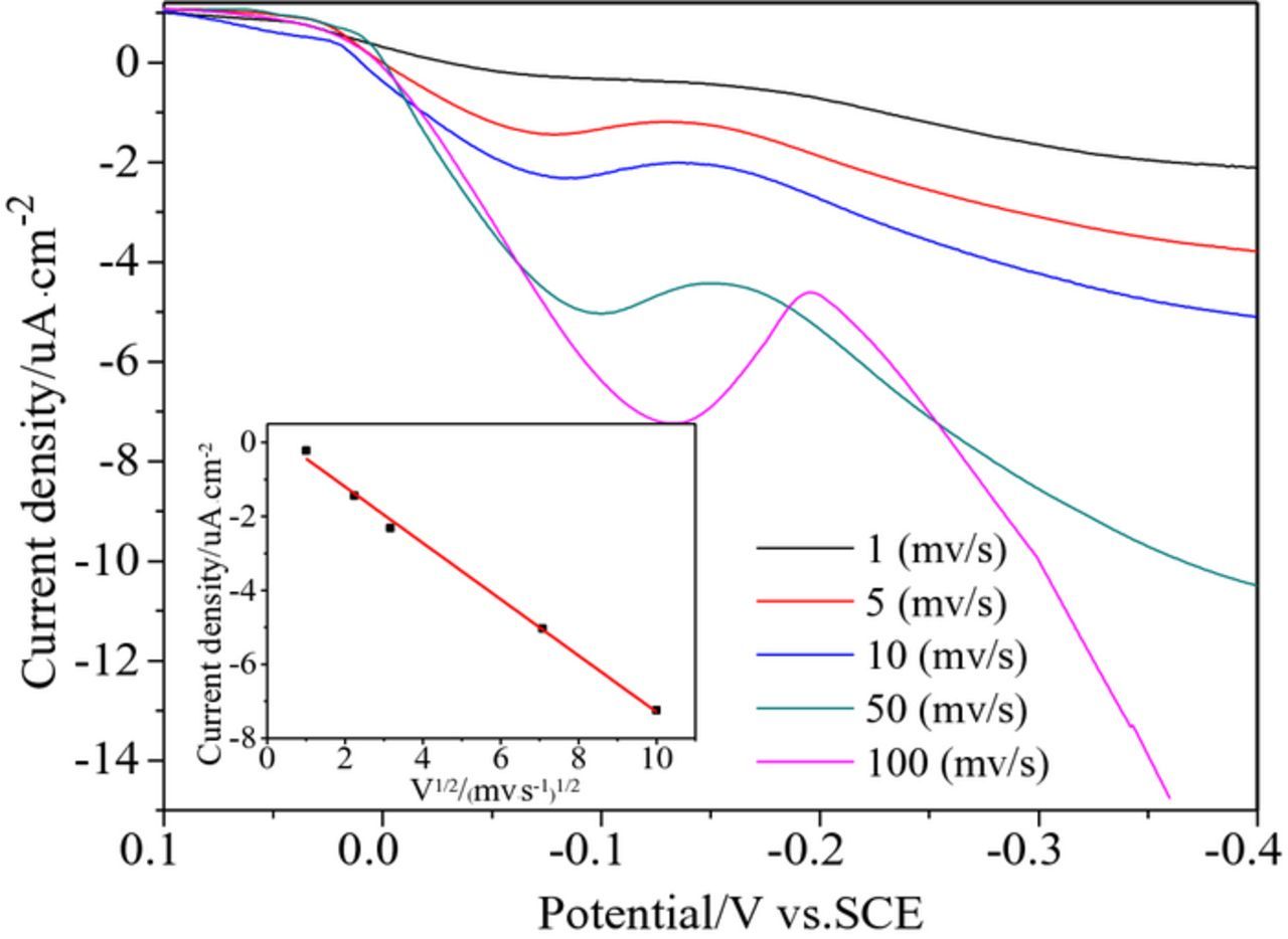
Figure 2. Cyclic voltammograms of Cu2O with different scan rates, the inset is fitted line plot.
The electrode kinetics of Cu2O deposition can be expressed by the Butler-Volmer Eq. 2
![Equation ([2])](https://content.cld.iop.org/journals/1945-7111/164/14/D999/revision1/d0002.gif)
Here, j is the current density (mA·cm−2), j0 is the exchange current density (mA·cm−2), and η is the overpotential (V). The exchange current density can be used to describe the ability to gain or lose electrons in an electrode reaction, and it reflects the difficulty of the electrode reaction. It can be described by Tafel curves. Fig. 3 illustrates a typical Tafel plot using a 0.1 M KCl and 10 mM Cu(AC)2 solution on an ITO electrode. The j0 value was estimated at 0.23 × 10⁻³ mA·cm−2. The exchange current density was relatively large, indicating that the electroactivity of Cu2+ in surface deposition is higher.26

Figure 3. Tafel plot corresponding to the electrochemical reduction reaction, the scan rate is 1 mV·s−1.
Fig. 4 shows the potentiostatic current transient curve of the electrodeposition of Cu2O on the ITO electrode in a 10 mM Cu(AC)2 solution. The deposition potential was −0.1 V, the reverse pulse potential was 0.3 V, and the pulse time was 100 s. The illustration in Fig. 4 shows that, during the first 100 s, the transient curve shape was a typical response curve of an electrochemical process of nucleation and growth without double layer charging. Due to the form of the new phase and the increase of nucleation number on the ITO electrode surface, the current increased rapidly. Each Cu2O crystal nucleus formed a diffusion zone. The current increased continuously with the expansion of these areas. The current reached its maximum when the surrounding diffusion fields exhibited coalescence. Then, the diffusion current of the electrode began to decay to equilibrium.27 The charges of the reduction process (QC) and oxidation process (QA) were calculated by integrating the reduction and the oxidation branches of the current transients curve. The values of QC and QA were 419.7 × 10⁻⁶ and 287.5 × 10⁻⁶C, respectively. The value of QC is greater than the value of QA, indicating that the electrodeposition process of Cu2O on ITO was irreversible.
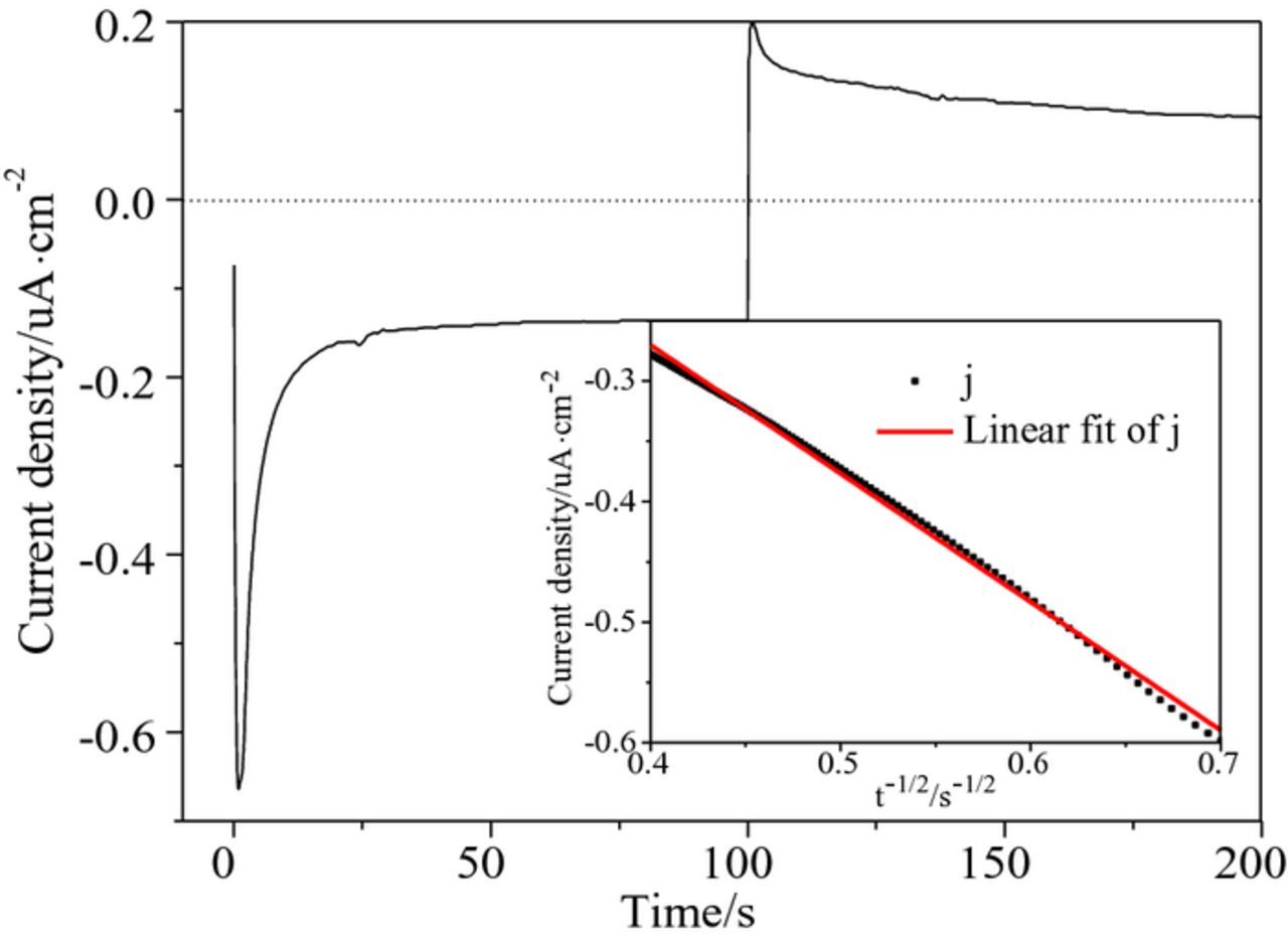
Figure 4. A potentiostatic current transient at a long time, the inset is the Cottrell plot.
The diffusion of electroactive Cu2+ in the solution can be quantitatively expressed by the diffusion coefficient (D). It can be estimated by analyzing the current density (j) of the direct pulse transient stage versus time (t) plot (Fig. 4 inset). The relationship between j and t satisfied the Cottrell Eq. 3 in the case of constant potential:
![Equation ([3])](https://content.cld.iop.org/journals/1945-7111/164/14/D999/revision1/d0003.gif)
Here, I is the current, n is the charge number (the value of n is 1), A is the effective area of the electrode (2.7 cm2), F is Faraday constant, and c is the concentration of Cu2+ in the solution (10 mM). Before the limiting current is reached, by drawing a Cottrell curve with |j| = f (t−1/2) on one axis, a linear graph should be obtained when the maximum width of the growing diffusion layer is achieved. Fig. 4 inset shows the linear part of the experimental Cottrell plot and the corresponding data fit. The diffusion coefficient was calculated by Cottrell curve data fitting. The value of D is 2.2 × 10⁻⁶cm2·s−1, which is the approximate diffusion coefficient of Cu2+as an electroactive substance in other solutions.28--30
Nucleation mechanism analysis of Cu2O
To further analyze the deposition mechanism of Cu2O on ITO electrode, the potentiostatic transient curves were recorded in different concentrations of Cu(AC)2, as shown in Fig. 5. Fig. 5 shows that the deposition mechanism of Cu2O can be analyzed by a Scharifker and Hills mathematical model of three-dimensional growth.31--33 Since the electrodeposition process of Cu2O is controlled by diffusion, the potentiostatic transient curves in Figs. 5a, 5b and 5c can be analyzed by the instantaneous nucleation Eq. 4 or the progressive nucleation Eq. 5 of three-dimensional growth
![Equation ([4])](https://content.cld.iop.org/journals/1945-7111/164/14/D999/revision1/d0004.gif)
![Equation ([5])](https://content.cld.iop.org/journals/1945-7111/164/14/D999/revision1/d0005.gif)
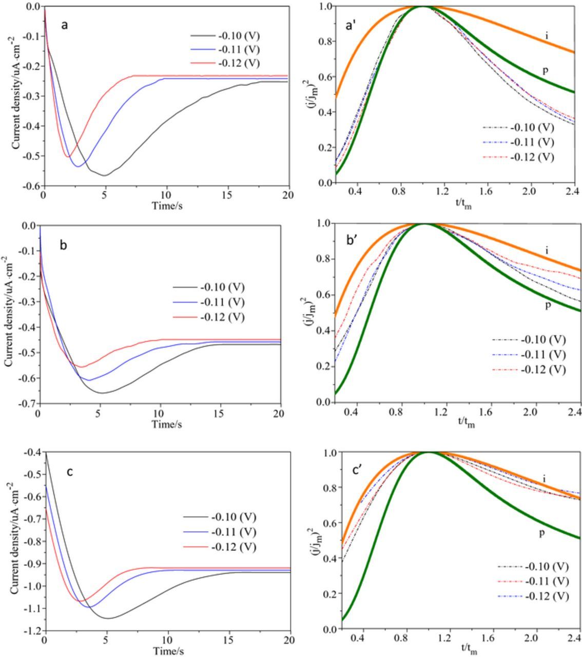
Figure 5. The potentiostatic current transients curves for electrodeposition Cu2O on ITO electrodes in (a) 5 mM, (b) 10 mM, and (c) 15 mM Cu(AC)2 solution, Figures 5a', 5b' and 5c' are corresponding non-dimensional plots of (j/jm)2 versus (t/tm).
Here, N0 is the nucleation density on the substrate surface (cm−2), A is steady state nucleation rate constant (s−1), K is the non-dimensional growth rate constant of crystal nucleus, and defined by K = (8πcM/)1/2.
To discuss the mechanism of the nucleation process, both experimental data and theoretical data were transformed to non-dimensional coordinate curves, normalized by the maximum current density (jm) and its corresponding time(tm). The experimental data of jm and tm were obtained from the potentiostatic transient curves, and the theoretical maximum values can be calculated by Eq. 6 for instantaneous nucleation and Eq. 7 for progressive nucleation
![Equation ([6])](https://content.cld.iop.org/journals/1945-7111/164/14/D999/revision1/d0006.gif)
![Equation ([7])](https://content.cld.iop.org/journals/1945-7111/164/14/D999/revision1/d0007.gif)
Therefore, the dimensionless Scharifker-Hills mathematical model can be expressed by Eq. 8 for instantaneous nucleation and Eq. 9 for progressive nucleation:
![Equation ([8])](https://content.cld.iop.org/journals/1945-7111/164/14/D999/revision1/d0008.gif)
![Equation ([9])](https://content.cld.iop.org/journals/1945-7111/164/14/D999/revision1/d0009.gif)
The potentiostatic current transient curves of Cu2O deposition in three different concentrations of Cu(AC)2 solutions are shown in Figs. 5a, 5b and 5c. Figs. 5a, 5b and 5c show that, with applied potentials applied, the current increased rapidly to its peak in the potentiostatic current transient curves under different conditions. Then it gradually decayed to a stable state and remained there. This is because, in the current rising process, Cu2+ discharge nucleation and the growth of crystals occurs on the electrode surface, and thus the cathodic current density increases. This reaction occurs until the current density has reached a peak of nucleation current density. Then, because of overlap between the crystal nucleus, the current attenuation reaches a balance between current increase and decay. Under the same deposition potential, the peak current and equilibrium current decreased with increasing Cu(AC)2 concentration. This shows that the discharge nucleation was enhanced and the nucleation number increased. Under the same Cu(AC)2 concentration, the peak current and its time of arrival increased with the increase of deposition potential. In addition, the time for the peak current to weaken to equilibrium prolongs, indicating that the duration of the crystal nucleus formation stage extends with the increase of deposition potential.
The non-dimensional plots transformed from the curves of Figs. 5a, 5b and 5c using Eqs. 8 and 9 are shown in Figs. 5a', 5b' and 5c'). In Figs. 5a', 5b' and 5c', the curves i and the curves p are the theoretical curves for instantaneous and progressive nucleation, respectively. In Fig. 5a' (5 mM Cu(AC)2), the nucleation process curves conformed well to the nucleation theory curve of the progressive nucleation at different potentials. In Fig. 5b' (10 mM Cu(AC)2) shows that the nucleation process fell between the progressive nucleation and instantaneous nucleation at different potentials. In Fig. 5c' shows that the nucleation mode on the ITO electrodes in a 15 mM Cu(AC)2 solution was close to the instantaneous nucleation at different potentials. This indicates that the electrolyte concentration has a significant influence on the nucleation mechanism of Cu2O, while the deposition potential has no obvious impacts. Table I shows the nucleation density of Cu2O under different deposition conditions. Table I shows that the nucleation density of Cu2O under the instantaneous nucleation mechanism is much higher than the nucleation density under the progressive nucleation mechanism. In the same nucleation mechanism, the nucleation density shows a decreasing trend with the decrease of the deposition potential.
Table I. The nucleation density of Cu2O thin film under different electrolyte concentration.
| 5 mM | 0.18977 | 0.07609 | 0.07350 |
| 15 mM | 6.46274 | 4.51206 | 2.90771 |
The structure and surface morphology analysis of Cu2O thin film
Fig. 6 shows the XRD patterns of Cu2O thin films at different electrolyte concentrations. All diffraction peaks for three samples accord well with the standard powder diffraction patterns of cuprite Cu2O (JCPDSNo.05-0667). The diffraction peaks were observed at 2θ 29.55°, 36.42°, 42.30°, 61.34°, 74.40°, and 77.75°, which correspond to the Cu2O (110), (111), (200), (220), (311), and (222) crystal planes, respectively. No other diffraction peaks were observed, indicating that pure Cu2O can be obtained through electrodeposition. Three samples were characterized by (111) crystal plane preferred orientation. This can be attributed to different growth rates along different crystal planes of the Cu2O crystal. This is because the value of the surface energy of Cu2O each crystal is (100) > (110) > (111). The high surface energy crystal face grows faster and the low surface energy crystal face grows slower in the vertical direction. Therefore the crystal faces of high surface energy decreased and the areas of crystal faces with low surface energy increased.34,35 Therefore, the prepared Cu2O in most cases has (111) preferential orientation. Fig. 6 shows that the diffraction peak intensities of the three samples were different. This may be related to the nucleation mechanism under different electrolyte concentrations. This indicates that the change of electrolyte concentration has little influence on the intensity of the diffraction peak, and it does not change the preferential orientation of Cu2O thin films. It has been proven that the (111) crystal plane of Cu2O has a high catalytic activity.36
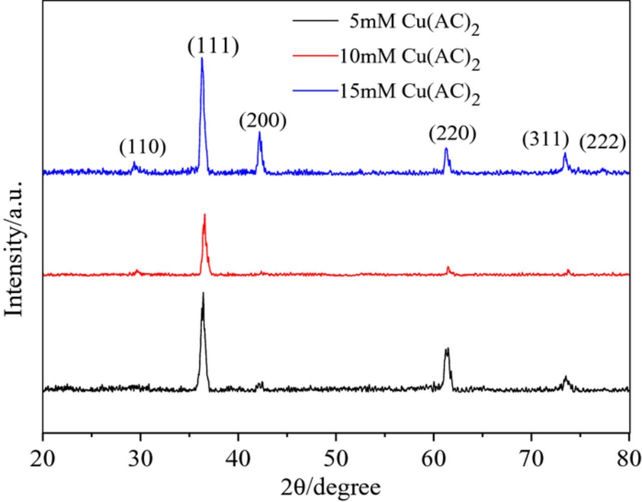
Figure 6. XRD patterns of the Cu2O thin films.
Fig. 7a shows the XPS spectra of the Cu2O thin film. Fig. 7a shows that there were Cu elements, O elements, and a small amount of adsorbed C elements in the samples. Fig. 7b, showing the Cu-resolution XPS spectra, shows that there were two peaks at 932.5 and 952.2 eV, which respectively correspond to the Cu 2p3/2 and Cu 2pl/2 binding energies of Cu2O. In addition, the FWHM at the peak energy for Cu 2p3/2 (1.2 eV) was not more than 1.5 eV, and the satellite peak does not appear between the Cu 2p3/2 and Cu 2pl/2 energy peaks, indicating that no Cu or CuO are present in the Cu2O thin film. Fig. 7c shows the O-resolution XPS spectra. Fig. 7c shows that there was a broad peak at 531.7eV corresponding to the O 1s binding energy, and the shoulder was not detected along with the peak, indicating that the basic elements of O come from Cu2O. Thus, the prepared Cu2O thin film shows high purity. This is consistent with XRD analysis results.

Figure 7. (a) XPS spectra, (b) Cu 2p XPS spectra, and (c) O1s XPS spectra of Cu2O thin film.
Fig. 8 shows the SEM images of the Cu2O thin films. The orientation characteristics of the three samples are clear from Fig. 8. Under instantaneous nucleation (Fig. 8c), the grains had a sword-like dendritic shape, and the crystal grains were regular in density. Under progressive nucleation (Fig. 8a), in addition to the sword-shape dendritic crystals, there were many irregular grains and the grain size was nonuniform. Fig. 8b shows that the surface morphology of the Cu2O was composed of dendritic crystals and irregular grains, and the grain size was relatively uniform.
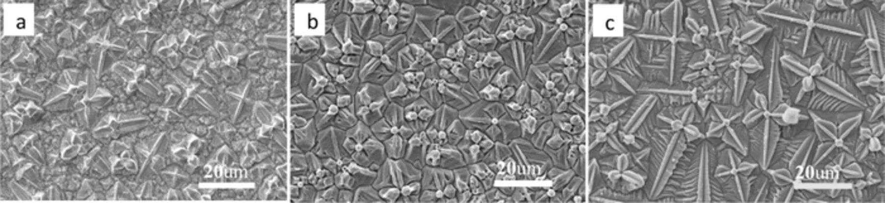
Figure 8. SEM images of the Cu2O thin films (a) 5 mM Cu(AC)2, (b) 10 mM Cu(AC)2, and (c)15 mM Cu(AC)2.
Optical performance analysis of Cu2O thin film
The UV-Vis diffuse reflectance spectra of the Cu2O thin film are shown in Fig. 9. Fig. 9 indicates that the absorption intensity of Cu2O thin films does not change with the change in electrolyte concentration, with the absorbing boundary at about 640 nm. The bandgap energy of the thin films can be calculated according to Eq. 1037
![Equation ([10])](https://content.cld.iop.org/journals/1945-7111/164/14/D999/revision1/d0010.gif)

Figure 9. UV-Vis spectra of Cu2O thin films, the inset is bandgap energy of Cu2O.
Here, A is absorbance, K is a constant, m is 1, photon energy (eV) for the abscissa, (Ahv)2 for the ordinate, taking the absorbing boundary tangent, the intersection of the tangent and the horizontal axis is the bandgap energy. Usually the bandgap energy between the valence band and the conduction band of semiconductors increases with the decrease in particle size.38 The bandgap energy of the Cu2O thin films were 2.006 (15 mM Cu(AC)2), 2.018 (10 mM Cu(AC)2), and 2.035 eV(5 mM Cu(AC)2), respectively. This result is consistent with the reported bandgap energy of Cu2O thin film. The Cu2O has the smallest bandgap energy under the instantaneous nucleation mechanism (15 mM Cu(AC)2), indicating that in this case the Cu2O has the largest particle size. This is consistent with the results shown in Fig. 8. This indicates that the nucleation mechanism has a slight effect on the bandgap energy of Cu2O thin film. The prepared Cu2O thin films can absorb solar energy effectively.
Fig. 10 shows the photoluminescence (PL) spectra of the samples, with the excitation wavelength at 360 nm. Fig. 10 shows that the PL spectra of the different samples were essentially identical in shape and position, indicating that electrolyte concentration does not have an influence on the shape and position of the PL spectra. The PL intensity of the prepared Cu2O in 15 mM Cu(AC)2 electrolyte was strongest, indicating that it had the best optical performance.39,40
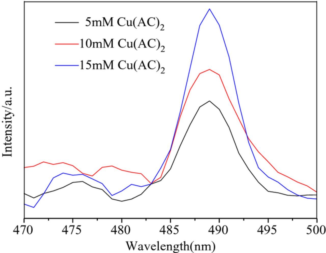
Figure 10. Photoluminescence spectra of the samples.
Electrochemical impedance analysis of Cu2O thin film
To find the charge carrier density of Cu2O, the Cu2O electrodes were characterized by electrochemical impendence spectroscopy (Fig. 11). The potential sweep was performed at a fixed frequency (1 kHz) with a scan speed of 10 mV/s. The charge carrier density can be extracted from the slope of the plot between the reciprocal of the square of capacitance per unit area (1/C2) versus the applied potential (V) according to the Mott-Schottky Eq. 1141,42
![Equation ([11])](https://content.cld.iop.org/journals/1945-7111/164/14/D999/revision1/d0011.gif)
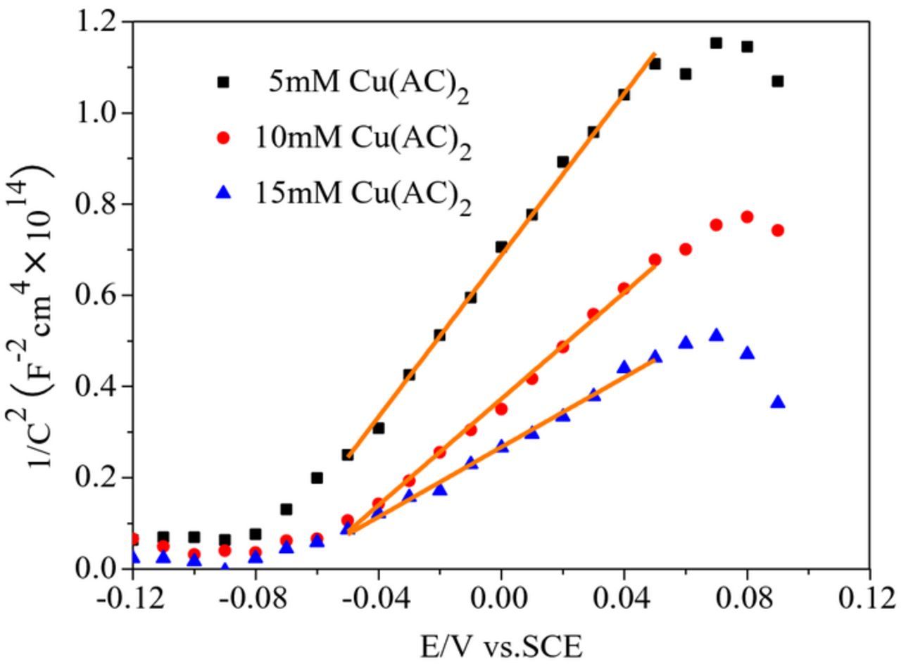
Figure 11. Mott-Schottky analysis of the samples in 0.5 M Na2SO4 solution.
Here, C is the charge layer's capacitance, e is the electronic charge, ɛ is the relative permittivity of Cu2O (ɛ∼7.5),43 ɛ0 is the permittivity of vacuum, A is working electrode area, ND is the charge carrier density, V is the applied potential, VFB is the flatband potential of semiconductor, KB is Boltzmann's constant, and T is the absolute temperature. According to Mott-Schottky theory, the slope of the linear region (linear part) of the Mott-Schottky curve is negative, indicating that the measurement sample is a p-type semiconductor and the hole is the majority carrier, while a positive slope reveals an n-type semiconductor where the electron is the majority carrier.
Fig. 11 shows the Mott-Schottky plot for the Cu2O electrodes in a 0.5 M Na2SO4 solution. Fig. 11 shows that the slopes of the Mott-Schottky curves of all three samples were positive, indicating that the three Cu2O thin films were n-type semiconductors.44,45 This indicates that the change of electrolyte concentration does not influence the conductive type of the prepared Cu2O semiconductor thin films. According to the Mott-Schottky Eq. 11 and Fig. 11, the estimated charge carrier densities of the Cu2O were 2.1 × 10²², 3.2 × 10²², and 4.9 × 1022cm−3 for the Cu2O thin films electrodeposited, when electrolyte concentration were 5 mM Cu(AC)2, 10 mM Cu(AC)2, and 15 mM Cu(AC)2, respectively. Under the instantaneous nucleation mechanism, the Cu2O has higher charge carrier densities. The highest majority carrier density of the Cu2O thin film signifies a fast charge transfer, and thus an enhanced photoelectrochemical performance.45,46
Nyquist curves can be used to analyze the process of charge transfer between the Cu2O electrodes and the electrolyte interface. Fig. 12 shows the Cu2O electrodes' Nyquist plots. The Nyquist plots were measured at an open-circuit potential of 0.005 V, with a frequency range of 10 kHz to 1 Hz under dark conditions. In Fig. 12, the points were experimental values, while continuous lines were simulated data according to the equivalent circuit. The equivalent circuit diagram is shown in the inset of Fig. 12, where Rs is the solution resistance, R1 is the charge transfer resistance of the electrode/electrolyte interface, R2 is the thin film resistance of the electrode, and CPE1 and CPE2 are constant phase components. The diameter of the semicircle indicates the interfacial charge transfer resistance R1 and thin film resistance R2.47 Table II shows that the fitted values of Rs were almost constant for all cases in the dark, which may be ascribed to deviations in the position of the reference electrode.48 The fitted values show that the thin film resistance follows the order of R2 (353.22 KΩ·cm2, 15 mM Cu(AC)2) < R2 (486.90 KΩ·cm2, 10 mM Cu(AC)2) < R2 (545.09 KΩ·cm2, 5 mM Cu(AC)2). The prepared Cu2O under the instantaneous nucleation mechanism shows the lowest R2 value. The fitted values of R1 were 127.27, 138.32, and 206.22 KΩ·cm2 for the prepared electrodes in 15 mM Cu(AC)2, 10 mM Cu(AC)2, and 5 mM Cu(AC)2 electrolytes, respectively. The efficient charge transfer at the interface between photoelectrode/electrolyte impeded the charge recombination and led to the high charge transport of electrons through the films.47,49 Thus, the prepared Cu2O electrode in the 15 mM Cu(AC)2 electrolyte has the lowest R1, showing a very good rate of charge transfer. The R1 of the prepared electrode in the 10 mM Cu(AC)2 electrolyte was only slightly larger than the prepared electrode in the 15 mM Cu(AC)2 electrolyte. Thus, the charge transfer rate of the both electrode were similar. It has been reported38,49 that a compact structure thin film exhibits much less charge transfer resistance than a porous one for the same chemical composition. Therefore, the difference of charge transfer resistance may be attributed to the differences of the surface structure of the prepared thin films under different nucleation mechanisms. This is consistent with the results of this experiment. The results show that the prepared Cu2O thin film has higher charge carrier densities and lower resistance under the instantaneous nucleation mechanism. This indicates that the nucleation mechanism has a significant effect on the charge carrier density and resistance of the prepared Cu2O thin film. Accordingly, the right choice of mechanism can help such thin films make more efficient use of solar energy and boost their prospects in practical applications.

Figure 12. Nyquist plot of the samples, the inset is the equivalent circuit.
Table II. Fitting parameters according to the equivalent circuit of Fig. 12.
| 5 mM | 5.3586 | 206.22 | 1.145 | 0.79605 | 545.09 | 0.85189 | 0.85979 |
| 10 mM | 5.2689 | 138.32 | 0.555 | 0.57434 | 486.90 | 0.4149 | 0.73327 |
| 15 mM | 5.3088 | 127.27 | 11.166 | 1.001 | 353.22 | 1.70 | 0.63166 |
Conclusions
The electrodeposition process of Cu2O thin film on ITO surface was studied by electrochemical techniques. The results show that the electrodeposition process of Cu2O is an irreversible diffusion-controlled process. The nucleation mechanism of Cu2O is associated with the electrolyte concentration. When the Cu(AC)2 concentrations are 5 mM and 15 mM, the nucleation processes of Cu2O fit the progressive nucleation and instantaneous nucleation theory models, respectively. The nucleation density under the instantaneous nucleation mechanism is much higher than the nucleation density under the progressive nucleation mechanism. For the same nucleation mechanism, the nucleation density decreases with as the applied potential decreases.
The nucleation mechanism of the Cu2O has a significant impact on the structure, morphology, and optoelectronic properties of Cu2O thin film. Under the instantaneous nucleation mechanism, the Cu2O crystal morphology is more uniform, with sword-shaped dendritic crystals, and the bandgap energy is 2.006 eV, less than the 2.035 eV under progressive nucleation mechanism. Compared with the progressive nucleation mechanism, the prepared Cu2O under the instantaneous nucleation mechanism shows stronger PL properties, higher carrier concentration (4.9 × 1022 cm−3), and smaller equivalent resistances R2(353.22 KΩ·cm2) and R1(127.27 KΩ·cm2). It exhibits a more regular morphology and superior photoelectric properties. However, the change in electrolyte concentration does not influence the conductive type of the prepared Cu2O. The Cu2O thin film has potential applications in the field of solar energy.
Acknowledgments
This work was supported by the National Science Foundation of China (Nos. 21576220, 21276208), the Natural Science Foundation of Shaanxi Province (No. 2015JZ005) and the Key Laboratory Research Project of Education Department of Shaanxi Province (No. 17JS085).