Abstract
Three-dimensional vanadium pentoxide (V2O5) material architectures in the form of inverse opals (IOs) were fabricated using a simple electrodeposition process into artificial opal templates on stainless steel foil using an aqueous solution of VOSO4.χH2O with added ethanol. The direct deposition of V2O5 IOs was compared with V2O5 planar electrodeposition and confirms a similar progressive nucleation and growth mechanism. An in-depth examination of the chemical and morphological nature of the IO material was performed using X-ray crystallography, X-ray photoelectron spectroscopy, Raman scattering and scanning/transmission electron microscopy. Electrodeposition is demonstrated to be a function of the interstitial void fraction of the artificial opal and ionic diffusivity that leads to high quality, phase pure V2O5 inverse opals is not adversely affected by diffusion pathway tortuosity. Methods to alleviate electrodeposited overlayer formation on the artificial opal templates for the fabrication of the porous 3D structures are also demonstrated. Such a 3D material is ideally suited as a cathode for lithium ion batteries, electrochromic devices, sensors and for applications requiring high surface area electrochemically active metal oxides.
Export citation and abstract BibTeX RIS

This is an open access article distributed under the terms of the Creative Commons Attribution 4.0 License (CC BY, http://creativecommons.org/licenses/by/4.0/), which permits unrestricted reuse of the work in any medium, provided the original work is properly cited.
The growth in portable electronics and the need for cleaner energy solutions has led to the rising interest in materials research and energy storage material architectures that may help drive advancement in energy storage technologies to mitigate current issues in some energy storage materials and batteries such as capacity fading and lower life times, for example.1–4 In recent years, three-dimensional (3D) material architectures5 have become a particularly attractive approach to achieving significant improvements in charge rate performance, maintenance of specific capacity and opportunities for higher power density supercapacitors.6–9 For this reason, the development of synthesis routes for the fabrication of three-dimensional nanostructured active materials onto metallic current collector substrates is important.10–13 Electrodeposition is a particularly facile route for the formation of metal and metal oxide films on a variety of conductive substrates and has recently gained a lot of attention for synthesising three-dimensional materials when combined with templates and sacrificial architecture-directing structures.14–17
Vanadium pentoxide is a particularly attractive replacement cathode material with its mixed valence, V4+ and V5+, making it an ideal candidate for a large number of redox-dependent applications. Vanadium pentoxide (V2O5) can be synthesized by a number of techniques, including hydrothermal synthesis,18,19 sol-gel techniques,20 chemical vapor deposition, and atomic layer deposition. However, the electrodeposition of vanadium oxides from VOSO4 aqueous solutions has the benefit of low cost and simplicity. The layered geometry of orthorhombic crystalline V2O5 makes it ideally suited to the reversible intercalation of mobile guest species,21,22 such as Li+ and other cations.23–26 While the lattice structure is theoretically maintained upon mild intercalation, phase changes are known to occur and the interlayer van der Waals spacing characteristic of its layered orthorhombic crystal structure can become deformed at lower voltages (higher Li mole fraction).27,28 Large particle sizes can also limit the solid state diffusional rate of cation insertion. The growth of a porous, three-dimensional V2O5 material, with space available to accommodate material expansion during Li+ insertion and significantly greater electrolyte wetting of the surface, is important for limiting and mitigating structural deformation, while simultaneously providing an increased surface area compared with a planar film to alleviate diffusion limited charge-discharge rates. Ordered materials that exhibit structural color may also enhance electrochromic characteristics and improve immobilization of species for (electro)catalysis29 or sensing. Preventing deleterious cracking in some Li-ion materials with hierarchically porous architecture may offset the trade-off with lower gravimetric and volumetric energy densities if the porous material is electrochemically and reversibly efficient through consistent electrical connection to the substrate or current collector.
The growth of vanadium oxide films through electrochemical oxidation is a well-established route and the use of templates during electrochemical growth for the fabrication of three-dimensional structures is gaining increasing interest.30,31 Here, the influence of different substrates (SS, ITO, Au-coated silicon) on the electrophoretic growth of the sphere template was examined. We then compared the electrodeposition of planar non-templated films of V2O5 with the electrodeposition of three-dimensionally porous V2O5 inverse opals using an aqueous ethanolic solution of VOSO4. The influence of the template on material growth and composition was monitored using X-ray diffraction, Raman scattering, X-ray photoelectron spectroscopy, and electron microscopy. Methods to alleviate electrodeposited overlayer formation on the artificial opal templates for the fabrication of the porous 3D structures are also demonstrated.
Experimental
Opal template fabrication
Colloidal crystal templates were formed on ∼1 cm × 1 cm of conductive substrates of stainless steel (SS) foil, ITO/FTO coated glass of ∼2 cm × 1 cm total area, or on Au-coated silicon substrates by the electrophoretic deposition of 200 nm, 350 nm or 500 nm diameter polystyrene (PS) spheres at a constant potential of 2 V or 3 V for 30 or 50 mins. The PS spheres from Polysciences Europe GmbH were functionalized with sulfate groups to aid in self-assembly. Sphere solutions were prepared using 0.8 mL of the 2.5 wt% sulfated PS solution mixed with 4.3 mL ethanol, and ∼80 μL of 30% aqueous NH4OH to ensure a pH between 8 and 10. This produced a final concentration of spheres of ∼0.4%. Electrophoretic deposition produced multilayer colloidal crystal opal PS templates with the hexagonal (111) plane grown parallel to the substrate surface, with better thickness control compared to drop-casting. Templates were then gently annealed for ∼2 h at 70°C to promote adhesion (necking of spheres) and structural stability for the subsequent electrodeposition step. Contact angle measurements were acquired for all opal templates on a Kruss Easy Drop measurement system using the static drop method.
Electrodeposition of vanadium oxide
Vanadium pentoxide was infilled by electrodeposition at room temperature using a VersaSTAT3 Potentiostat. A constant potential of 2 V was applied versus a saturated calomel (SCE) reference electrode in a three-electrode cell with a platinum mesh as counter electrode and the PS template-coated substrate as the working electrode. This is schematically outlined in Fig. 1.30,31 The electrolyte consisted of a 0.25 M VOSO4.χH2O solution in 1:1 (v/v) mixture of deionized water and ethanol. The final solution was made by adding 2.53 g of VOSO4.χH2O, used as purchased from Sigma Aldrich, to a mixture of 20 ml of deionized water and 20 ml of ethanol. The addition of ethanol to the solution reduces the surface tension between electrolyte and the PS template, increasing infiltration of the electrolyte to substrate surface.30,31
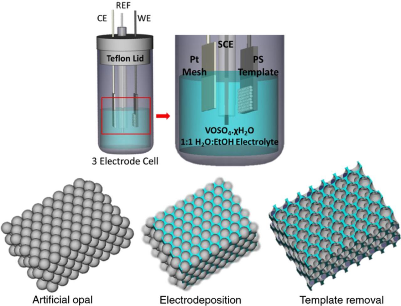
Figure 1. Schematic diagram of the three electrode cell used for the electrodeposition of vanadium oxide into the 3D artificial opal template of PS spheres.
After deposition, samples were heated to 300°C for 24 h to remove the spheres, resulting in the formation of a network of crystalline V2O5. A temperature of 300°C was deemed optimum based on morphological and Raman scattering examination of the structure uniformity and crystal phase purity. For instance, heating for shorter time at 450°C resulted in regions of the opal template that were irregular and spatial inhomogeneity in oxidation state was found. The 24 h calcination period in air allowed gentler decomposition of the polymer and release of CO and CO2 gases without rupture to the underlying porous material. The electrodeposition of vanadium oxide was performed for PS templates on ITO-coated glass, Au-coated Silicon and stainless steel (SS) foil substrates. For comparison, vanadium oxide was also electrodeposited under similar conditions on to substrates without PS templates in place. These planar deposits were also heated at 300°C for 24 h to ensure the formation of crystalline V2O5. The mass of SS changes slightly on heating due to oxide formation, and so all SS substrates were therefore pre-heated to 300°C and allowed to cool before sphere deposition to improve the accuracy of the mass calculation. Limited thermal oxide growth (blueing) on SS post-deposition was not found to influence the adhesion of the planar nor IO structures that were electrodeposited.
Structural and elemental characterization
Structure and morphology characterization of the electrodeposited IO materials after sphere removal was performed using an Hitachi S-4800 field emission scanning electron microscope (FESEM). Elemental and compositional information was investigated using Raman scattering spectroscopy, X-ray diffraction (XRD), and X-ray photoelectron spectroscopy (XPS). Raman scattering was performed with a Renishaw InVia Raman Spectrometer using a 30 mW Ar+ laser at 514 nm excitation. The beam was focused onto the samples using a 50× objective lens and spectra were collected using a RenCam CCD camera. X-ray diffraction was performed on a Philips Xpert PW3719 diffractometer using Cu Kα radiation. XPS analysis was conducted on an Oxford Applied Research Escabase XPS system using a non-monochromated Al-Kα X-ray source at 200 W. Core level scans were acquired at a take-off angle of 90° and were charge corrected with respect to the C 1s photoelectric line. A step size of 0.1 eV, dwell time of 0.5 s and pass energy of 20 eV averaged over 50 scans was used. A Shirley background correction was employed and peaks were fitted to Voigt profiles using CasaXPS software.
Results and Discussion
Opal template electrophoretic deposition
Electrophoretic deposition of thick opals films using 350 nm spheres at 2.0 V for 30 mins produced very well ordered fcc arrangements with very few cracks, as seen in Fig. 2a. Cracking during drying of opal films is exacerbated by ordering defects or vacancies in lateral and vertical sub-structure. Previous work has identified the influence of deposition time at a given voltage, for opal template formation.32 Additional deposition approaches involving white noise during dip-coating methods,13,32,33 spin-coating techniques34 or other assembly approaches to minimize crack formation have been reasonably successful.33,35–38 We have found that an increase in voltage to 2.5 or 3.0 V does affect ordering on a SS substrate (Figs. 2b and 2c), while deposition at 2.0 V on other conducting substrates such as ITO (Fig. 2d) and Au-coated Silicon wafers (Fig. 2f) results in lower crack density, but greater order-defect density. Thus, a higher number of ordered domains are found on ITO and Au-coated silicon after formation at 2.0 V, but much fewer macroscale cracks are observed. Contact angle measurements in Fig. 2 confirm that the top surface of the sphere assemblies in all cases is relatively uniform and a high (>75°) water contact angle is maintained. The square packing of the spheres is found to be a characteristic of electrophoretic opal formation and more prevalent at higher voltages, and with smaller sphere sizes at the same voltage (not shown). This arrangement is indicative of a domain with (100) orientation at the surface interspersed with domains of dominant (111) orientation. On ITO and SS surfaces (which tend to be more hydrophilic than Au-coated Silicon), defects in the packing order without sphere vacancies, result in domain boundary formation in otherwise tightly packed opal template deposits.
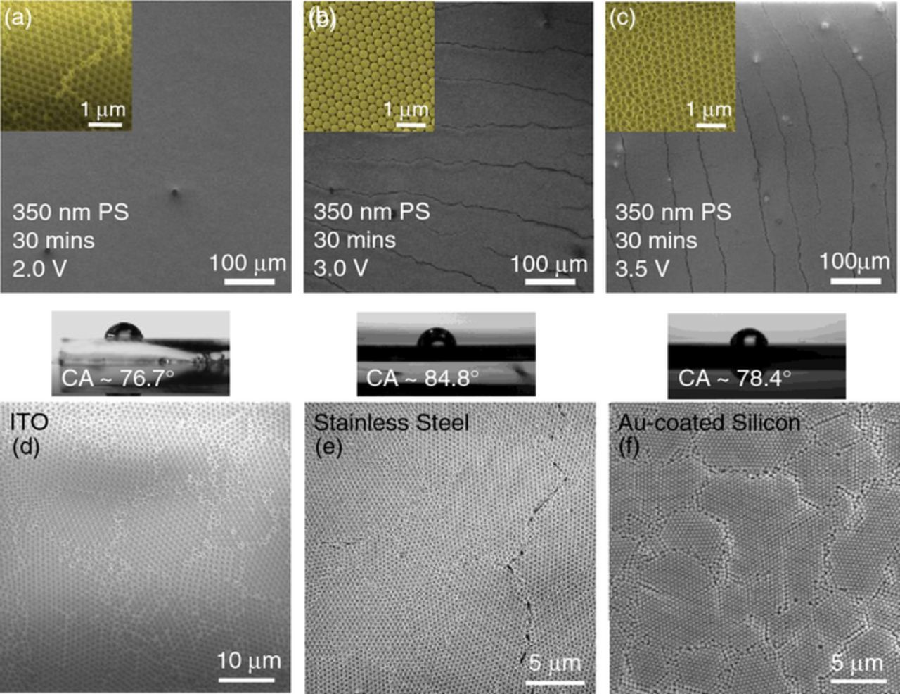
Figure 2. (Top) SEM images of the electrophoretically deposited 350 nm PS sphere artificial opal templates on ITO for 30 mins at (a) 2.0 V, (b) 3.0 V, and (c) 3.5 V. (Bottom) Plan-view SEM images and contact angle water droplets for opal film top surfaces after deposition at 2.0 V on (d) ITO, (e) SS, and (f) Au-coated Si(100).
Chronoamperometry
In order to compare the growth and nucleation characteristics of the templated and non-templated electrodeposited material, chronoamperometric current density-time transients were recorded throughout the electrodeposition process. Current density-time curves for a 3D template and planar substrate electrodeposition are shown in Figs 3a and 3b at a constant voltage of 2.0 V for 15 mins. In both depositions the current initially rises from a non-zero value due to instantaneous nucleation as the size and/or number of growth nuclei increases, thus expanding the electroactive area. The current begins to decrease once the electrode surface becomes saturated due to coverage by V2O5 and the rate of nucleation and growth gradually lowers toward steady state growth. This deposition profile is characteristic of 3D growth via continuous nucleation, and the template coverage of the electrode surface does not alter the electrodeposition mechanism. The profile observed for the templated V2O5 material (red) is similar in overall profile to that of the material grown on a bare substrate (black curve). In Figs. 3a and 3b, both curves exhibit a non-zero current, rapid rise to a limiting current, the formation of a peak and a more gradual decay to a relatively constant current. Consistently, the current for 3D-template IOs of V2O5 are 40–50% lower than deposition on a planar substrate of equal area, which is consistent with the expected coverage (or exposed inter-sphere regions) by a hexagonal (111)-opal layer comprised of 350 nm spheres. Thus, a lesser volume of V2O5 formation is formed per unit time consistent with a lower active surface area (and interstitial volume fraction in the opal) and electrode screening by the spheres. In a simple diffusion controlled process, the Cottrell equation,39
![Equation ([1])](https://content.cld.iop.org/journals/1945-7111/162/14/D605/revision1/d0001.gif)
can be used to describe the current-time relationship and in certain cases determine a value for the diffusion coefficient, where I is the current, n is the number of electrons transferred, F is Faradays constant, A is the area of the electrode, C*0 is the concentration of the electroactive species, t is the deposition time and D is the diffusion coefficient for the species.40,41
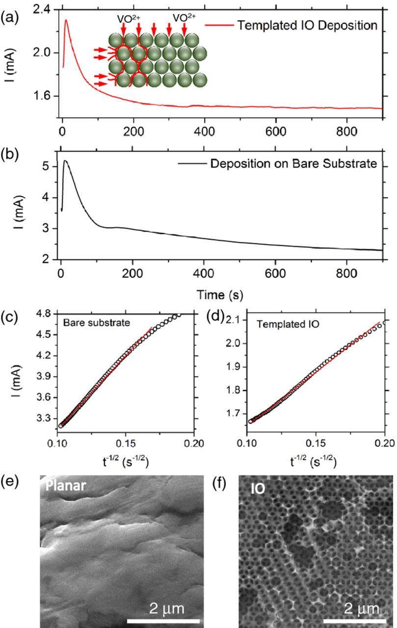
Figure 3. Characteristic current (I) versus time chronoamperograms observed for deposition (a) into a PS sphere template on stainless-steel foil substrate and on to (b) bare stainless-steel foil and current (I) versus t−1/2 for the decreasing portion of the i vs t transients for electrodeposition (c) into a PS template on stainless steel and (d) onto bare stainless steel. All electrodeposition was conducted at 2 V for 15 mins. SEM image for (e) planar V2O5 electrodeposited film and (f) the IO deposit.
This value corresponds to the V2O5 subsequently nucleated and grown on the already formed V2O5 from the initial polarization and electrodeposition on to the available substrate surface. To account for cracks, domain boundary defects, and some (100) packing in opal ordering (thus increasing accessible volume in some cases), this value is taken as a lower bound value. A deposition according to:
![Equation ([2])](https://content.cld.iop.org/journals/1945-7111/162/14/D605/revision1/d0002.gif)
is also assumed and therefore the number of electrons involved in the half-cell reaction (n in Eq. 1) is considered to be 2. The electrolyte used here typically had a pH ∼ 2.2 at room temperature. By comparison with Potiron et al.,42 the final phase formation is not analyzed here through a 4-electron process whereby precipitation of the insoluble intermediate species occurs if the pH is considerably higher than 1.8, according to
![Equation ([3])](https://content.cld.iop.org/journals/1945-7111/162/14/D605/revision1/d0003.gif)
![Equation ([4])](https://content.cld.iop.org/journals/1945-7111/162/14/D605/revision1/d0004.gif)
The total deposition time and electrolyte volume prevent significant acidification of the electrolyte.
In the electrodeposition process, the trends observed for both the templated (Fig. 3a) and planar (Fig. 3b) V2O5 confirm a diffusion-controlled growth. The Cottrell equation (Eq. 1) can be applied to the decreasing portion (after the current peak) of the current-time transient by determining the functional relationship between the current i vs t−1/2; a linear relationship is indicative of a diffusion-limited process in this region. Mass transport of reactants is thus limited by the diffusion of cationic V-O species following the sulfate solubilization within the double layer at the surface of the growing V2O5. In Figs. 3c and 3d the two Cottrell plots are shown, and SEM images of the planar and IO material are shown in Figs 3e and 3f. A similar trend is seen for electrodeposition onto the SS foil with a PS opal template (Fig. 3c) as for the bare SS substrate (Fig. 3d). The slope differs as expected due to the variation in growth volume and current caused by the template, but the template appears not to affect the mechanism of nucleation and acts as a structural mould for shaping the 3D continuous nucleation and growth in time.
The current plateau after the initial nucleation and wetting of each surface in the region of the current peak, shows consistent volumetric increase of V2O5 in time at a constant formation rate. Using the slopes of Figs 3c and 3d of ∼4.64 × 10⁻³ A·s1/2 for the templated deposition and ∼21.3 × 10⁻³ A·s1/2 for the bare substrate, and factoring the effective interstitial volume fraction Vf = 0.26, of an (infinitely thick) fcc opal available to the ions, the diffusion constants Dfcc = 5.21 × 10⁻⁷ cm2 s−1 and Dsoln = 4.25 × 10⁻⁷ cm2 s−1 are found to be similar.
Here, Dfcc is related to the diffusion coefficient of the VO2+ species diffusing toward a planar electrode, Dsoln, by the relationship
![Equation ([5])](https://content.cld.iop.org/journals/1945-7111/162/14/D605/revision1/d0005.gif)
where Vf is defined above and τ is the tortuosity of the diffusional path of ions through the non-linear interstitial voids of the opal template lattice,43,44 as depicted in Fig. 3a. We assume for the following analysis that the maximum packing is achieved for a (111)-oriented surface of an fcc opal and that initially, the flux of all ions is toward the substrate via the nominal electric field, but from the top and sides of the opal since it is soaked in electrolyte. From geometric considerations, it is generally accepted that conformal growth within a fcc artificial opal creates air pockets occupying ∼3.5% of the remaining space, i.e. maximum possible infilling is ∼96.5%. This limitation is overcome since the infilling is not a sphere-surface conformal coating, but a bottom up complete infill. The tortuosity in opals was previously examined in numerical simulations and shown to be anisotropic and to vary with lattice direction, such that the rate of molecular transport normal to the (111) plane is ∼10× less than diffusion in the bulk electrolyte. The tortuosity had a value of τ = 3.0 based on finite element simulations of molecular transport through (100), (110) and (111) lattice vectors of an opal.45 However, this analysis assumed that the electrolyte ion approach each of these planes solely; any opal with a (111) surface will also have dissimilar cross-sectional lattice faces. Additionally, as Newton et al. confirm,45 the void fraction tends to 0.26–0.28 for all three low index planes (particularly (111)) when opals comprising more than 10 layers are used, which satisfies our experimental electrophoretically deposited opals (that comprise several tens of sphere in thickness and also in width.32 We chose the estimation of comparative diffusivities of electroactive species to examine the effect of electrode surface coverage and tortuosity of the opal on the electrodeposition at a constant voltage. This avoids variation in the growth mechanism at different voltages in voltammetric analyses of diffusion in the framework of the Randles-Ševčík relation as a function of potential scan rate.46 Using the Eq. 5, the experimental measured tortuosity is just τ = 0.21, an order of magnitude less than previously estimated. As the effective diffusion constants above are very similar, the opal thus does not significantly limit ionic diffusion in a well-soaked maximally packed fcc opal. The ratio of measured currents in the diffusional regime (via slopes of Figs 3c and 3d) is ∼0.22. Thus, electrodeposition of vanadium oxide inverse opal reported here is not limited by the packed structure of the opal template and the nucleation and growth mechanism follows that of planar electrodeposition. The reduced currents scale with the reduction in available free volume of the packed structure.
Structure of electrodeposited V2O5 inverse opals
The bottom-up filling of the sphere template can be advantageous and useful in preparing IOs.47 Material congestion in the upper layers of the template tends to be problematic in some approaches where top down infilling is used, particularly those involving liquids or solutions that need to wet the entire active 3D porous surface. For instance, atomic layer deposition infilling of opal templates has recently been adopted to facilitate conformal filling of interstitial spaces within the template with functional materials.48,49 Electrodeposition of structured materials within templates using the parameters reported here facilitates complete bottom-up infilling via continuous nucleation and growth. However, effective nucleation and coverage of the initial bare surface is critical for good electrical contact for subsequent use and to prevent delamination during drying by anchoring the full inverse opal to the electrode surface. This approach offers a facile and improved infilling method that does not necessitate vacuum infiltration for liquid-based precursors, and thicker deposits, volumetric densities are therefore possible and controllable with electrodeposition.32
The bottom-up approach provides other challenges which are also investigated. Electrodeposited material formation in IOs or other porous material templates can also occur at the surface of the template i.e. those areas of the substrate in contact with electrolyte by a preferential nucleation mechanism. At lower current densities, issues due to discontinuous infilling are well known, and at current densities that promote continuous material infilling, a thick, sealing overlayer of the material on the template surface can often form. When using a sphere template atop a conductive substrate the available electrode surface are interstitial sites within the opal template and in the preferred case, growth and nucleation continues around and within the template.50,51 It is possible however, for growth to occur parallel to the substrate beneath the regions occupied by the template. In such cases, this deposition may reduce template adhesion leading to separation from the substrate before complete electrodeposited infiltration of the entire template. Detachment from the substrate is also seen when material thickness grows to a large mass, effectively pulling the template from the substrate. In this work, this effect was particularly prevalent for depositions of ≥1 h (corresponding to a 3D IO structure thickness >18 μm) on all conductive substrates investigated. Deposition time must therefore be calibrated to suit the template thickness. Excessive deposition times at the same voltage results in an overfilling of the template, producing a porous V2O5 IO structure trapped beneath a dense non-porous layer of V2O5, as shown for samples on ITO-coated glass in the SEM images in Figs. 4a and 4b.
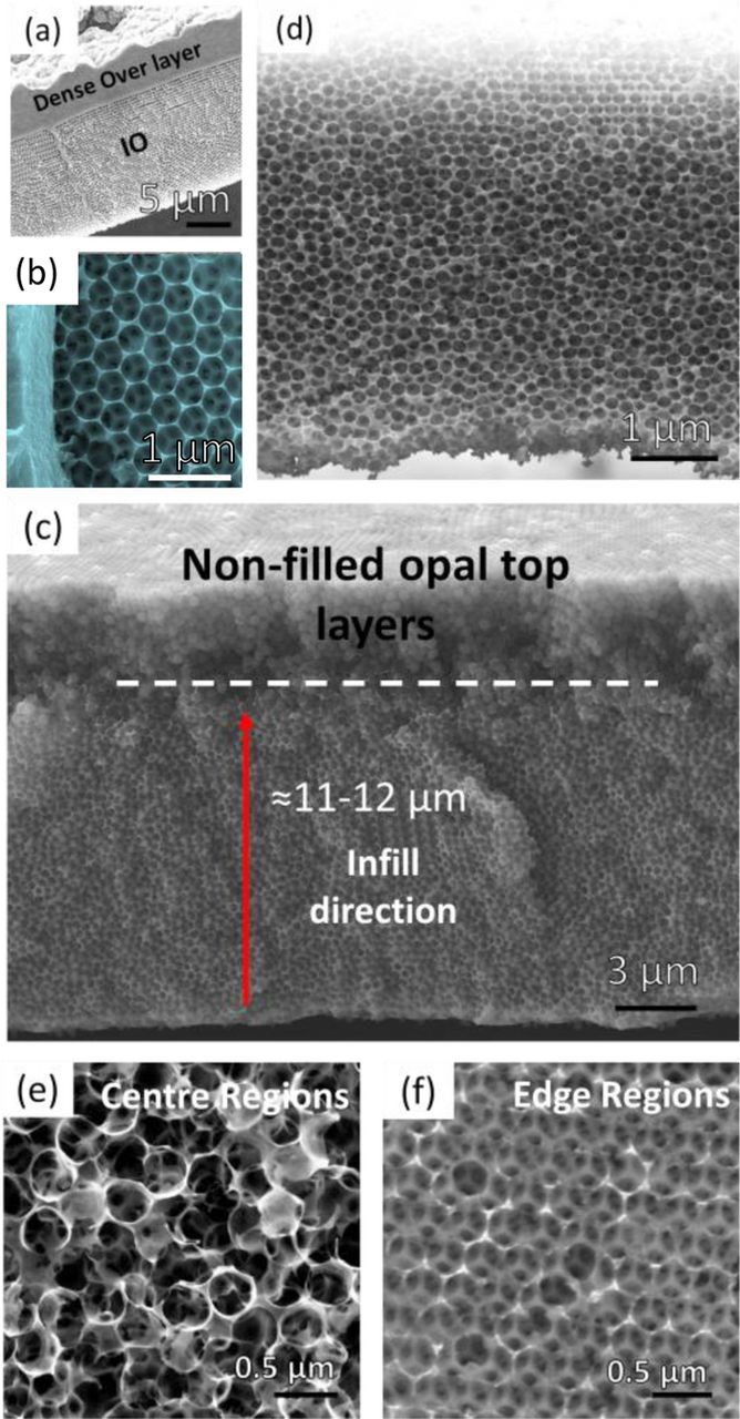
Figure 4. SEM images of the V2O5 IO structure after infilling of PS sphere templates on ITO–coated glass by electrodeposition at 2 V showing (a) and (b) the excess material atop the IO structure from an extended infill time of 1 h. Cross sectional SEM images of (c) a PS template on stainless steel substrate infilled at 2 V for 15 min before removal of the spheres, indicating only a partially filled template with a remaining area of unfilled sphere layers at the top (above white dashed line) and (d) the IO structure after removal of the spheres and material crystallization for ∼24 h at 300°C. (e) SEM images of the disordered but highly porous IO network observed at regions near the centre of the sphere template and (f) the better ordered areas near the top and side edges for a sample on SS foil.
To reduce the possibility of template overfilling and/or detachment from the substrate, deposition times were restricted to 15 min. Electrophoretically deposited template formed at 3 V for 30 min, are usually infilled to a level just below the total template thickness (see Fig. 4c) after 15 min, leaving several layers of spheres in the template surface visible after removal from the electrolyte. In this way, completely infilled, open IO structures that are more conducive to electrolyte infiltration were formed with thickness of ∼10–12 μm, shown in the cross sectional SEM image in Fig. 4d. The unfilled opal layers at the top of the template are thus sacrificed to ensure an open topped 3D inverse opal. By preventing complete infiltration, nucleation and continued growth of the overlayer is prevented using electrodeposition parameters that are preferential to infilling from the substrate upwards.
The two central morphologies observed in an IO structure formed at 2 V for 15 min on SS foil are presented in Figs. 4e and 4f. SEM analysis revealed the formation of three-dimensional macroporous structures separated into an island like arrangement by structural voids characteristic of crack propagation and material contraction that occurs during sphere removal and sample drying.52,53 Networked material close to the centre of the template appeared more disordered (Fig. 4e) than those formed near the electrolyte meniscus line and outer edges of the sample, which maintained the structural order of the opal template (Fig. 4f). It is unclear whether the disorder within the sample structure is as a result of the deposition process or as result of sphere removal. At regions along the meniscus, template thickness is often thinner than the template bulk due to a thin liquid region within a meniscus, thus reducing the density of spheres available for deposition during EPD as well as overall solution settlement during the process. It could be speculated that the disruptive removal of the unfilled layers of spheres causes the surface disorder in the centre regions of the IO compared with the edge areas. Accurate filling of a self-assembled opal template of indeterminate thickness (or variable thickness) may require further work for accurate control of electrodeposition kinetics and time.
Crystallinity and phase purity of electrodeposited V2O5 inverse opals
Raman scattering spectra were measured for the electrodeposited IO material and the material deposited without an opal template after heating to 300°C for 24 h. The Raman spectra for the IO material can be indexed to the orthorhombic structure of crystalline V2O5 with a space group Pmnm and D2h point symmetry. The characteristic Raman modes of crystalline orthorhombic V2O5 at 102, 145, 196, 285, 304, 404, 482, 526, 701, and 994 cm−1 are observed. The stretching mode associated the short vanadyl V=O bond,54 of bond length 1.58 Å, is well defined at 995 cm−1, and the vibration associated with the layered nature of V2O5 at 145 cm−1 is the most prevalent. Raman scattering data taken from the material deposited without a template before heating is shown in Fig. 5a. The spectrum resembles that of the IO V2O5 material but with broader peaks at much lower intensities with some variation in peak position. The broadness of the peaks, particularly the V-O-V stretching vibrations between 280–750 cm−1 illustrates the predominantly amorphous nature of the as-deposited material. The poorly defined peak at 990 cm−1 and the peak at wavenumber 1019 cm−1 are associated with the V=O vanadyl stretching vibration. The higher ionic radius of V4+ accounts for a higher bond length than that of V5+ leading to a lower vibrational frequency, therefore the peak at 990 cm−1 corresponding to a bond length of 1.60 Å can be attributed to V4+ and the peak at 1019 cm−1 with bond length 1.58 Å to V5+.56,57 Such peaks have also been observed in V2O5 hydrated xerogels and their respective positions above and below the standard frequency for the V5+ = O vibration of crystalline V2O5 (usually ∼995 cm−1) attributed to the effect of crystal water molecules within the van der Waals layer spacing of the V2O5 matrix material.58 The low intensity and broadness of these peaks in the as-deposited spectrum generally is attributed to the low crystallinity and predominant amorphous phase of the as-deposited material.16,59 Heating of the as-deposited material reduces the level of hydration and oxidizes the V4+ ions to V5+ creating a single vanadyl stretching vibration peak corresponding to a short bond length of approximately 1.58 Å.
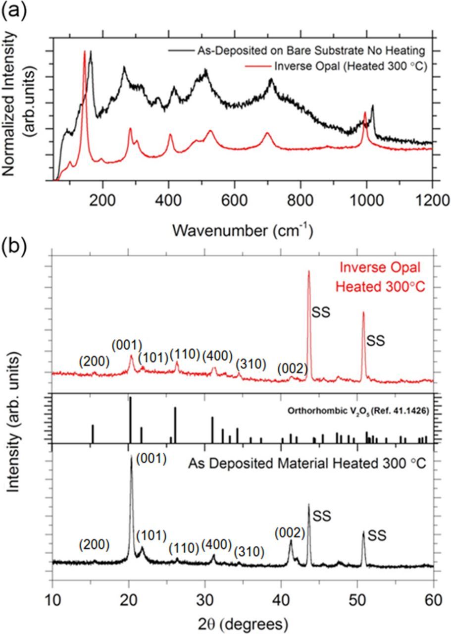
Figure 5. (a) Raman scattering data for the IO material (red) and the as-deposited material (black) (b) XRD spectra for the inverse opal material (red) and the as-deposited material (black) once it is heated to 300°C for 24 h compared with the orthorhombic V2O5 reference spectrum (line graph). SS indicates diffraction peaks from the stainless steel substrate.
The XRD pattern (Fig. 5b) obtained for the electrodeposited IO structure (red pattern) resembles that of bulk crystalline V2O5, with the (001) peak at 2θ ≈ 20.37° and corroborates the classification of the material as orthorhombic V2O5 with space group Pmnm. No clear XRD pattern was obtainable from the as-deposited (with or without template) material due to its predominantly amorphous nature. However, after heating for 24 h at 300°C the as-deposited material (black pattern) produced a well-defined pattern indicative of crystalline orthorhombic V2O5. Calcination removal of spheres by this method is effective and no remnant PS is found. Additionally, the crystalline quality is excellent, and effective removal of the entire template through the brittle IO material is possible at temperatures just above the decomposition temperature for PS.
The marked intensity difference from (001) reflection for the heated as-deposited material compared with the IO material can be attributed to the differences in nanostructure of the as-deposited thick films compared with the porous nano-walled IO structure. The nanoscale sub-structure of the walls of the crystalline IO limit the intensity of reflections from the characteristics (001) interlayer spacing of orthorhombic V2O5. In such structures, the Scherrer relation provides an estimate of the effective crystallite size L = 0.94λ/βcos θ where λ is the X-ray wavelength (1.54 Å), β is the line broadening or FWHM (in this case of the (400) peak), and θ = the Bragg angle. An average crystallite size L of ∼20–25 nm for the nanoscale crystalline sub-structure of the IO material within the walls of the IO, and correspondingly, ∼90–100 nm for the heated as-deposited film.
XPS measurements were carried out to compare the as-deposited material before and after heating on the bare substrate to the IO V2O5 obtained after heating at 300°C for 24 h to crystallize and remove the spheres, and the core level spectra are shown in Fig. 6. The color of the as-deposited V2O5 is typically dark green/black while the IO material exhibits a bright yellow color, the as-deposited material has a dull yellow or red-brown appearance once heated to 300°C for 24 h, and these characteristic colors are symptomatic of a variation in oxidation state or level of hydration in the materials. Note, these colors do not have a angle-dependent structural color contribution in their description from neither 2D Bragg (grating) diffraction nor 3D pseudo photonic bandgap from the IO – the colors are correlated to the materials' oxidation states.
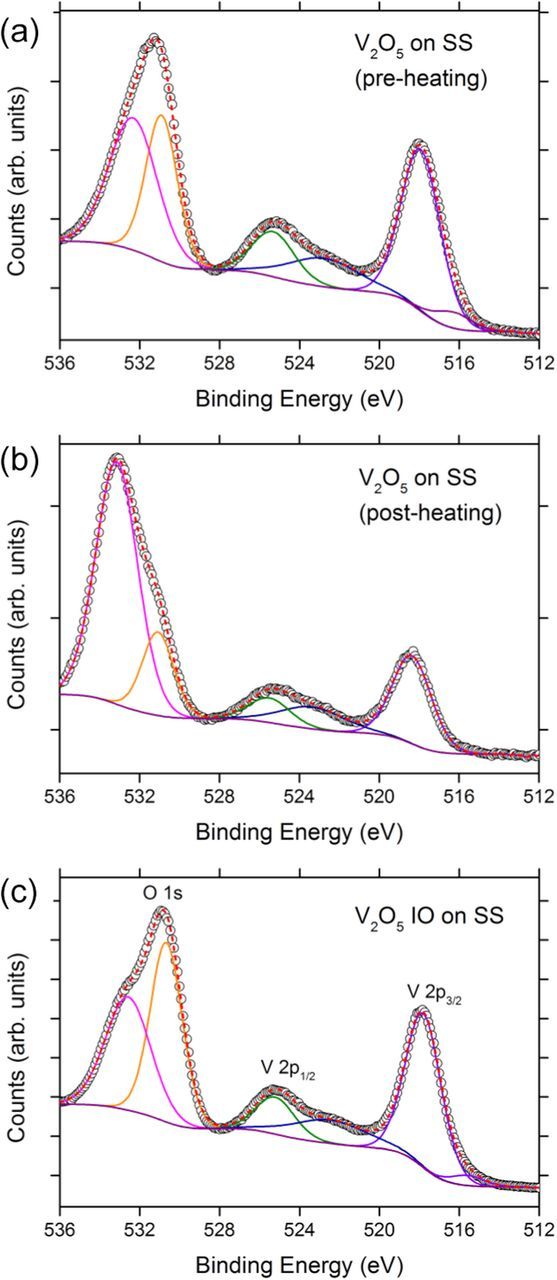
Figure 6. V 2p and O 1s core-level photoelectron emission spectra from the electrodeposited V2O5 material (a) on the bare substrate before heating (b) on the bare substrate and heated to 300°C for 24 h and (c) the IO material obtained after deposition in a sphere template on the SS substrate.
In general, the XPS results corroborate both Raman and XRD data, confirming both the IO and as-deposited materials, as V2O5. The V 2p3/2 core-level photoelectron peak corresponding to the presence of V5+ appears at ∼518 eV for the as-deposited material electrodeposited on to the bare substrate (Fig. 6a) while the V 2p3/2 core level emission for the as deposited film of V2O5 IO is found at ∼518.5 eV after 24 h at 300°C (Fig. 6b); details are summarized in Table I. This V 2p3/2 core level emission shifts to ∼517.9 eV for the electrodeposited IO material (Fig. 6c). The V 2p1/2 core-level occurs at similar energies for the IO material (525.3 eV) and for the material deposited without a template both before (525.4 eV) and after heating (525.6 eV).
Table I. XPS data acquired form planar electrodeposited V2O5 films and from V2O5 IOs on SS.
| Electrodeposition/ | O 1s (eV)/ | V 2p3/2 (eV)/ | |||
|---|---|---|---|---|---|
| Structure | Treatment | [fwhm] | [fwhm] | Δ (eV) | Surface Phase |
| V2O5 on SS | 2.0 V | 530.9 [2.78] | 518.0 [2.59] | 12.9 | V2O5 |
| V2O5 on SS | 2.0 V / 300°C | 531.1 [2.82] | 518.4 [2.62] | 12.7 | V2O5 (with –OH termination) |
| V2O5 IO | 2.0 V / 300°C | 530.7 [2.52] | 517.9 [2.39] | 12.8 | V2O5 |
The O 1s emission consists of two components in all three cases, at binding energies of 532.6 and 530.7 eV for the IO material, at ∼532.4 and 530.9 eV for the as-deposited material and at ∼533.2 and 531.1 eV for as-deposited material heated to 300°C for 24 h in both cases, corresponding in all three cases to oxygen ions in the V-O-V and V-O-H groups, respectively. The oxidation states determined from the V 2p and O 1s core-levels can be estimated according to 13.82 − 0.68 [O 1s − V 2p3/2].60,61 The average vanadium oxidation state was calculated to be 4.912 for electrodeposited IO structure, and 5.116 (thus V5+) for the non-templated planar V2O5 film. Thus, electrodeposition allows the formation of crystalline V2O5 with orthorhombic layered structure and a dominant pentavalent oxidation state.62 Electrodeposited IO V2O5 retains predominantly monovalent structure as a crystal and within the surface phase even in a structure with a much greater surface area, which typically exhibit di- or multivalent character.
Conclusions
This work illustrates a route for the fabrication of high quality, open 3D crystalline V2O5 inverse opals on several conductive substrates by electrodeposition using an aqueous solution of VOSO4.χH2O and electrophoretically deposited artificial opal templates. Opal templates are uniformly deposited on each of the conductive substrates, and high quality opal films are formed using 350 nm PS spheres at 2.0 V. Through chronoamperometry, electron microscopy, X-ray diffraction and photoelectron spectroscopy, the growth and formation of the V2O5 IO material was compared in detail with as-deposited planar electrodeposited V2O5 films deposited without an artificial opal template. Analysis of chronoamperometric polarization confirms a progressive nucleation mechanisms for V2O5 electrodeposition on planar as well as artificial opal-templated surface. Electrodeposition facilitates the fabrication of a bulk-like, single crystalline monovalent V2O5 phase via electrodeposition at a nanoscale length scale with complete coverage of the substrate and conformal template infilling. The influence of ionic mobility retardation due to opal template tortuosity, and coverage of the conducting substrate with the template, was demonstrated to be negligible. Electrodeposition of an IO is a function of the internal interstitial volume once conditions for conformal nucleation and continued growth are met. A strategy to successfully avoid overlayer growth was demonstrated, involving electrodeposition infilling (conformal from the bottom up) several sphere lengths short of the top surface, leaving an open topped 3D inverse opal without an overlayer. This type of structure and material is suitable for use in lithium ion battery cathodes to facilitate improved ionic diffusion and electrolyte infiltration and shorter solid state diffusion lengths, and allow the incorporation of secondary active phases within the porous regions through sequential (electro)deposition methods, and many other uses. Electrodeposited IO structures may also provide active materials for gas sensing, electro and thermochromics materials on a range of current collectors, substrates and surfaces.
Acknowledgments
E. A. acknowledges the support of the Irish Research Council under award RS/2010/2920. We acknowledge financial support from the IRC New Foundations Award. M. O. S. acknowledges financial support from the Royal Society of Chemistry Nuffield Award bursary. Support from Science Foundation Ireland (SFI) under grant no. 07/BK/1232a-STTF11 is also acknowledged. This work was also supported by SFI under the National Access Programme (NAP 417), through an SFI Technology Innovation and Development Award under contract no. 13/TIDA/E2761. This publication has also emanated from research supported in part by a research grant from SFI under grant Number 14/IA/2581.