Abstract
Understanding the nature of defects and their role on fundamental physical properties of semiconductors is essential to obtain the necessary material control to reach the full realization of their technological potential. High-resolution infrared measurements in combination with high-sensitive SIMS of unintentionally doped GaN films unambiguously identified Si and O shallow donors and yielded their ground state binding energies. High-resolution, variable-temperature photoluminescence studies of recombination processes associated with excitons bound to donors leaving the donors in the ground states and excited states after exciton annihilation are in excellent agreement with the energies of donor intra-impurity transitions measured by infrared absorption. Photoluminescence studies of unintentionally doped and doped GaN films clarified conflicting aspects of donor identification and binding energies of shallow pervasive Si and O donors. These results provided the experimental foundation for the detection and identification of pervasive shallow donors in GaN by optical methods.
Export citation and abstract BibTeX RIS

This is an open access article distributed under the terms of the Creative Commons Attribution 4.0 License (CC BY, http://creativecommons.org/licenses/by/4.0/), which permits unrestricted reuse of the work in any medium, provided the original work is properly cited.
Continuous progress in chemical vapor deposition (CVD) and molecular beam epitaxy (MBE) methods for epitaxial growth of GaN in combination with the development of intermediate nucleation layers led to successful fabrication and commercialization of increasing number of devices despite the previous lack of native substrate.1,2 The high deposition temperature required for growth of this wide bandgap semiconductor increases fundamental material problems such as thermal expansion and lattice mismatch, residual strain, incorporation of low-energy defect formation, and reactors residual impurity incorporation. In addition, dopant activation and self-compensation are difficult to control at high deposition temperatures. Presently, heteroepitaxial GaN is routinely deposited on sapphire, Si, and SiC substrates despite the relatively large mismatch in thermal coefficients and lattice parameters. These mismatches are released by the formation of dislocations with density typically between 108 cm−2 and 1010 cm−2.3,4 Hydride vapor phase epitaxy (HVPE), a vapor deposition method employing hydrochloric acid (HCl), which has a growth rate of about two to three orders of magnitude higher that CVD or MBE, was successfully employed to deposite thick GaN films directly on sapphire wafers or on CVD GaN/Sapphire templates.5 Substrate wafer engineering yielded freestanding (FS) GaN wafers with dislocation density as low as 106 cm−2. Independent of the epitaxial growth method, all unintentional doped (UID) films were n-type with room temperature free carrier concentration typically between low 1017 cm−3 to medium 1018 cm−3.
Several models were suggested to explain the large background concentration of room temperature free electrons observed on UID heteroepitaxial GaN. Previous calculations have indicated that nitrogen vacancies (NV) could behave as the active donor.6 However, Van de Walle and co-workers first-principle calculations showed that the formation energy of NV is too high to allow the incorporation of such a high concentration of donors during growth.7 More recently, impurities such as oxygen (O) and silicon (Si) have been identified as the pervasive background shallow donors in GaN films.8 Based on this identification, recent modifications of the materials used in the reactor liners resulted in a reduction of the free carrier concentration to low 1015 cm−3.9 It is expected that such break throughs will allow the development of a new types of electronic devices.
In the present manuscript, we review the results of our systematic investigation carried out on CVD, MBE, HVPE GaN films, and on UID and doped homopetitaxial films deposited on UID FS-HVPE substrates. These results yielded the identification of the chemical nature and binding energies of the pervasive donors in GaN. Variable temperature photoluminescence and Fourier transform infrared (FTIR) transmission experiments in combination with high sensitivity secondary ion mass spectroscopy measurements were employed to achieve our goal.
Experimental
The GaN films investigated in this work were grown by organometallic vapor phase epitaxy (OMVPE), on a-plane sapphire substrates and on crack-free FS UID-HVPE GaN substrates of size 10 mm × 10 mm, with thicknesses ranging from 150 to 400 μm. After a standard cleaning procedure, the substrates were placed in the MOCVD reactor, and the films were deposited at temperatures of approximately 1020°C under 1.6 SLM NH3 and 2.4 SLM H2, at a pressure of 130 Torr. Once the temperature stabilized, 27 μmol/min of trimethylgallium (TMGa) was introduced and the films were grown to a thickness of ≤5 μm. Si-doping was accomplished under the continuous flow of TMGa with a flow rate of 13 μmol/min. Five ppm of SiH4 was used, which resulted in films with electron mobility >600 cm2/Vsec.10 The MBE films were deposited by the RF-plasma assisted method in a Vacuum Generator VG80H MBE system equipped with an EPI Uni-Bulb nitrogen plasma source and in situ reflection high-energy electron diffraction (RHEED) capability. A 1.2 μm thick layer of UID GaN was grown on a 250 μm thick, 10 mm × 10 mm, FS n-type (UID) HVPE GaN substrate. After the conventional cleaning procedures, the substrate was placed on an indium-free mounting and loaded in the analysis chamber for out-gassing for 30 min at 700°C under UHV conditions. The substrate was allowed to cool to room temperature, and transferred to the deposition chamber. The substrate was then heated to the growth temperature of 625°C, over ∼45 min. Before opening the gallium shutter, the substrate surface was first exposed to the nitrogen plasma for 60 sec. The nitrogen plasma was maintained at 250W with an N2 flow of 0.80 sccm, and the growth proceeded in the gallium-rich regime as evidenced by a dim, streaky RHEED pattern and the gallium droplets on the as-grown surface. The growth rate under these conditions was ∼1 Å/sec.11
Photoluminescence (PL) is a well-established, highly sensitive, non-invasive and non-destructive technique to detect and identify native and impurity related point defects and their complexes in semiconductors. Characterization by PL involves the measurement and interpretation of the spectral distribution of recombination radiation emitted by the samples. Photon-generated electrons and holes usually become localized or bound at an impurity or intrinsic defect before recombining, and the identity of the localized center that they were bound at can often be determined from the luminescence spectrum. Qualitative information about the crystal quality can be inferred from the efficiency and line full-width-at-half maximum (FWHM) of near band edge emission spectra. Impurities can sometimes be identified based on the binding energies inferred from the spectral positions of free-to-bound transitions. In general, due to the presence of various radiative and/or non-radiative recombination channels competing for the photon-generated electron-hole pairs, luminescence processes cannot be conveniently used as a reliable quantitative technique. In the present work, low and variable temperature PL measurements were carried out with the samples placed in the chamber of a liquid He cryostat with temperature ranging from 1.6 to 320 K. The luminescence was excited with the 325 nm line of a HeCd laser, with power density that was controlled with calibrated neutral power density filters. The sample emission was collected with f-number matching optics and dispersed by a double grating 0.85 meter spectrometer fitted with a UV-extended GaAs photomultiplier connected to a computer controlled photon-counter. Narrow spectrometer slits were used to achieve the required spectral resolution for this experiment, and a spectral band-pass between 70 and 100 μeV was commonly employed. The spectrometer calibration was verified with standard lines from a mercury calibration pen lamp.
FTIR absorption is also a non-destructive technique with the important advantage of quantifying neutral electrically active donors and acceptor concentrations. Absorbed photons with energies equal to the energy necessary to promote electrons or holes from the ground state to the excited states produce an optical signature of the donors and acceptors. Assuming that the excited p-like states are bound to by an energy that depends weakly on the nature of the donor or acceptor, the ground-to-excited state transitions of different donors or acceptors are displaced by approximately the difference between their ground state binding energies. The IR measurements were carried out with the sample and detector placed in a light-pipe, which was filled with low pressure He gas for improve thermal contact and insert in a liquid He bath. The samples were thinned and wedged to minimize interference fringes and over-absorption. The average sample thickness (of the thicker sample) after wedging was about 145 μm.
SIMS measurements were carried out to identify and to measure the concentration of impurities incorporated in our samples. The SIMS depth profile results indicated that HVPE samples used in our experiments contain different amounts of impurities that are expected to be electrically active if they occupy the substitutional lattice sites. SIMS measurements were used in combination with with FTIR measurements to provide complete information on the nature and concentration of the pervasive shallow donors in GaN films and an optical signature of these impurities.
Results and Discussion
The low temperature spectra of UID CVD and HVPE thin (≤10 μm) GaN films typically showed intense recombination emission lines associated with the annihilation of excitons (with heavy hole valence band "A") bound to neutral donors (DoXA) and their longitudinal optical (LO) phonon replicas (nLO-DoXA). Also commonly observed are weaker non-phonon lines from shallow-donor/shallow-acceptor pair (DAP) recombination and their LO phonon replicas (nLO-DAP). Broad luminescence bands observed near 3.0 eV and 2.25–2.5 eV are discussed elsewhere.12–14 The free carrier concentrations of such films are typically in the order of low to medium 1017 electrons/cm−3, and their DoXA exciton FWHM is about 2.0–2.5 meV. Temperature dependent PL measurement shows that the high-energy shoulder of the DoXA is associated with recombination process involving the free-exciton associated with the heavy mass hole band (FEA). PL spectrum of thicker UID HVPE GaN with improved crystalline quality and reduced free carrier concentration background show the presence of a number of new recombination processes. Figure 1 depicts the PL spectra of a ∼12 μm thick HVPE GaN/Al2O3 template (Sample 1) from a provider 1 and a ∼150 thick FS HVPE film (Sample 2) from a provider 2. The spectrum of Sample 2 shows, in the 3.52 to 3.46 eV spectral region, emission lines related to the excited state of the free-exciton A (FXA2), the ground state of the free-exciton B (FXB1), the ground state of the free-exciton A (FXA1), and the dominant exciton bound to a neutral donor DoXA. Around 3.45 eV we detect the so-called two-electron satellite (2ES) spectrum resulting from the recombination process in which the neutral donors are left in an excited state after the exciton annihilation. Note that for energies below 3.42 eV, we observed the one-phonon replicas of all features listed above. The PL spectrum of Sample 1, the dotted line spectrum, shows most of the major features observed in the spectrum of Sample 2. However, these features are broader and smeared, and shifted to higher energy (by about 6.2 meV) due to inhomogeneous broadening and compressive strain, respectively, resulting mostly from the substrate.15 Figure 2 depicts four PL spectra of Sample 2 acquired with higher resolution at 5K under several laser excitation intensities, as indicated in the figure. The dominant features in all spectra are emission associated with the recombination of ground state excitons bound to neutral donors (often designed I2o, or DoX) cetered around 3.4714 eV. The dominant peak shown in Figure 2 is composed of three peaks at 3.4714, 3.4719, and 3.4723 eV, which we assign to A excitons bound to three neutral donors.16 To identify the chemical nature of these three background donors we carried out Fourier Transform Infrared (FTIR) absorption and high sensitivity SIMS measurement in a set of samples previously characterized by high-resolution PL spectroscopy.16,17
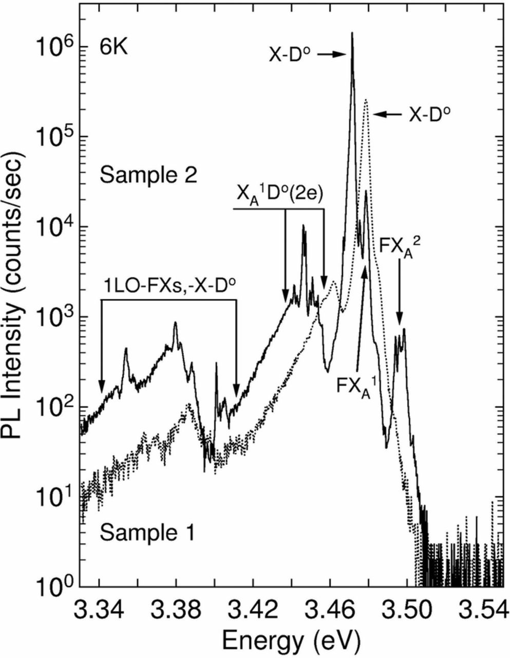
Figure 1. LT PL spectra of a ∼12 μm heteroepitaxial film (Sample 1, light-gray line) and of a ∼150 μm thick FS HVPE GaN (Sample 2, continuous line) films. The presence of a number of sharp exciton related recombination processes indicate the high quality of both samples. After, Freitas et al., Reference 15.
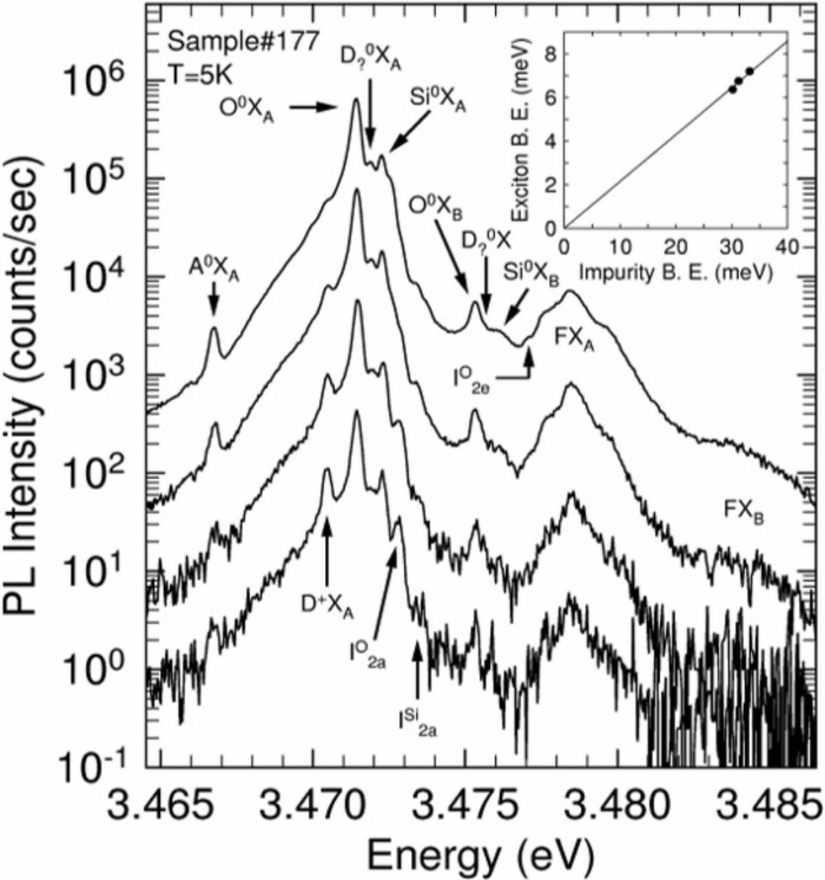
Figure 2. Low temperature PL measurements acquired with laser power densities of 61.1 (top curve), 8.4, 0.80, and 0.08 W cm−2 (bottom curve). The insert depicts the plot of the binding energies of the three donor-bound excitons versus the neutral donor binding energies. After Freitas et al., Reference 24.
The detailed FTIR measurements of impurity excitation absorption and SIMS determination of impurity concentrations were carried out for two previously selected HVPE GaN samples: a 10.5 μm thick sample (Sample 1) on a sapphire substrate and a FS 145 μm sample (Sample 2). These two UID samples, but nominally n type, were carefully selected from 15–20 GaN films because the PL and FTIR absorption of their dominant shallow donor was not the same. Figure 3 depicts the relative transmittance of both samples. Note that three lines (N1, N2, and N3) were observed in the spectrum of Sample 2. We considered SiGa, CGa, ON, and SN as the potential candidates for shallow impurities. Sulfur concentration in both samples were at the SIMS detection limit, and was ruled out as a candidate for any of the observed donors. Our initial expectation that either Si or O would dominate was confirmed by these studies. The weak third donor (N3) absorption, present in low concertation, has not been identified. Both samples gave clean impurity 1s-2p± excitation spectra with narrow line widths and only small amount of over absorption, as seen if Figure 3. It has been found that ground states of shallow donors and acceptors in semiconductors have a much greater impurity-to-impurity variation in binding energy than the p-like excited states.18 Consequently, the shallowest uncompensated donor has the smallest 1s-2p± transition energy. Here, the shallowest uncompensated donor is designated N1. A quantitative measure of the IR absorption strength for each donor was extracted by converting these transmission spectra into absorption coefficient spectra and determining the area of each donor 1s-2p± absorption coefficient peak, which are proportional to the concentration of neutral chemical species of the absorbing donors.
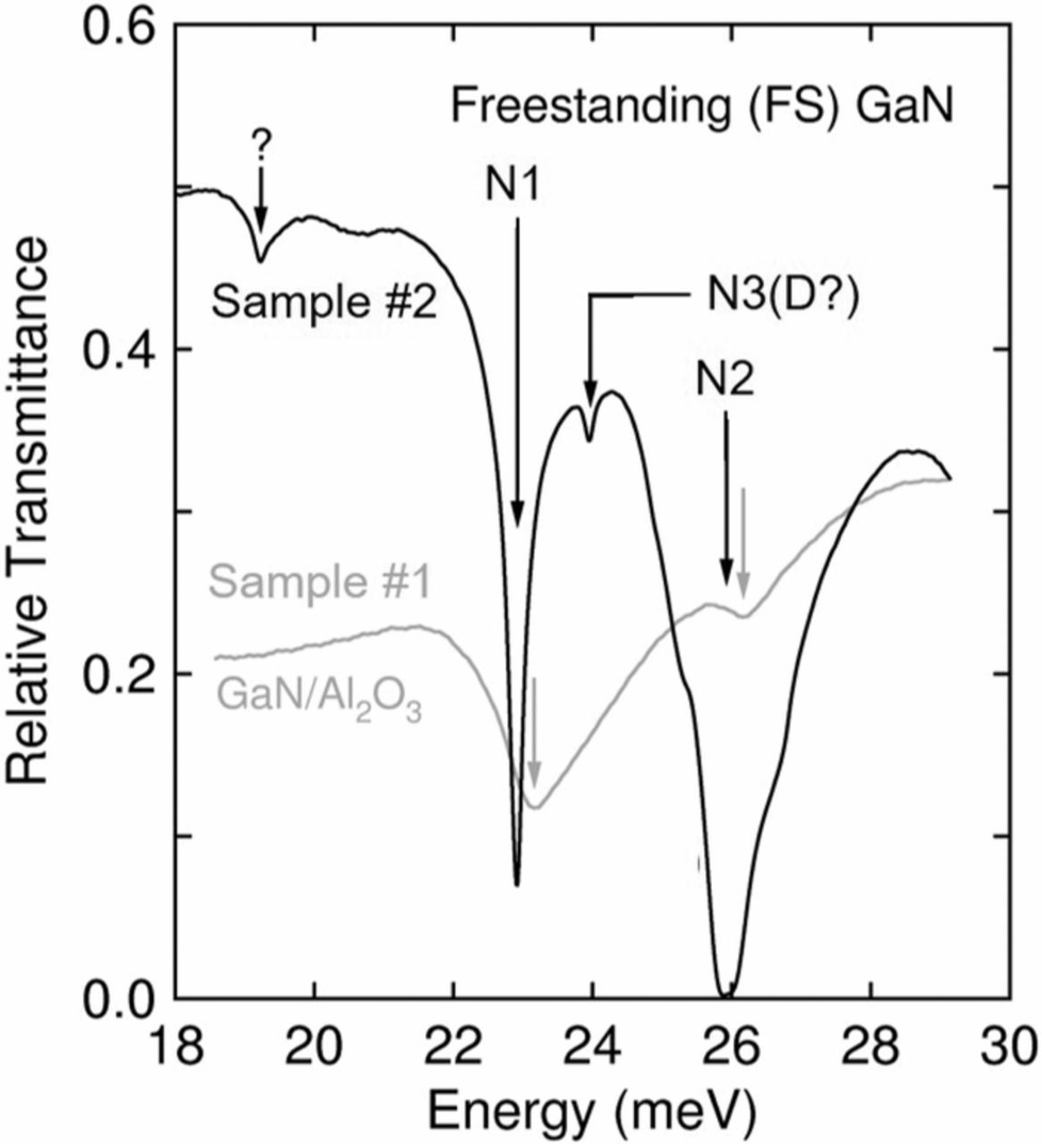
Figure 3. FTIR transmission spectra of Sample #1 (GaN/Al2O3) and Sample #2 (FS-HVPE). Note the change in the relative intensity of the lines N1 and N2. The unidentified transition at 19.3 meV, marked as "?" has been assigned to widely separated pairs or triads. After Freitas et al., Reference 36.
The O and C concentrations are about the same in both samples, ∼2 × 1016 cm−3 and ∼6–8 × 1015 cm−3, respectively. Note that the C concentrations are near the detection limit so the actual concentration may be substantially lower. Si concentrations are ∼1.2 × 1017 cm−3 and 3.7 × 1015 cm−3 in sample 1 and 2, respectively. Considering the absorption strength should be comparable to the ratio of Si observed in both samples, N2 cannot be SiGa. This leaves ON and CGa as candidates for N2. The concentrations of O in both samples are about the same, consistent with the IR absorption strength. C SIMS concentrations are about one third those of O, and C is expected to preferentially enter in GaN on the N site as an deep acceptor.19,20 Therefore, we identify O as the N2 donor. The IR absorption from N1 in Sample 1 exceeds that of N1 in Sample 2 by a factor of ∼34, while the SIMS concentrations for Si in Sample 1 exceeds that of Sample to by a factor of ∼32. Therefore, we identify N1 as Si.8
Donor 2p± and 3p± excited states more closely match the effective mass models than do donor ground states. We have used this fact to determine the 2p± binding energy for donors in GaN. Summing the measured 1s-2p± transition energy and the 2p± binding energy gives 30.18 ± 0.1 meV and 33.20 ± 0.1 meV, respectively, for optical activation energies of Si and O donors in GaN. The unidentified N3 donor has an activation energy of 31.23 ± 0.1 meV. Measurements carried out for activation energies between 14 and 29 meV, in both samples, exclude the presence of additional neutral donors at significant concertation in these samples. Magneto-optical studies were carried out in Sample 2 to investigate the ground-to-excited transitions in the IR for the Si, O, and the unidentified donor as a function of the magnetic field up to 11 Tesla.21 It was found out that the ground state binding energy of the effective mass in GaN is 29.1 ± 0.1 meV, and the separations rates for the 2p+ and 2p- excited states with the magnetic field are consistent with an electron effective mass of 0.22m0, in agreement with previously reported results.17,22,23
The PL line assignments shown in the power-density excitation spectra highlighted in Figure 2 are in excellent agreement with the FTIR study. Plot of the binding energies of the three donor-bound excitons, as determined from the PL, versus the neutral donor binding energies, as measured by FTIR transmission, depicted in the insert of Figure 2, yields a linear dependence between these two energies. This result follows the empirical Haynes rule with a linear coefficient of 0.214, which is close to the previously reported value of 0.2 ± 0.01.24,25 To verify the energy values of shallow-donors binding energies obtained from the IR study we carried out a detailed spectral analysis of the 2ES emission region. Figure 4 depicts the 2ES spectra of Sample 2 measured at 5K, 7K, 15K, and 25K. The 5 K spectrum was fitted with 16 lines, including the broad background features, is also represented in Fig. 4. All major features observed in Figure 4 have been identified and donor excited states inferred from the 2ES features have been compared with donor features measured in IR transmission. Agreement between these two techniques, summarized in Table I, is better than 250 μeV. The inferred 2s-2p splitting is 0.33 meV. This value is in reasonable agreement with calculation of the O 2s core shift using the 1/n3 rule (0.51 meV) that has been found to be approximated well in semiconductors.26 The present assignments differ from those proposed by Reshchikov describing PL measured at 15K on similar FS-HVPE GaN samples.27 This discrepancy indicates that the 2ES spectra are dominated by recombination from the excited donor-bound excitons at 15K and above, not from the unexcited donor-bound excitons. Therefore, to calculate the donor ground-to-excited-state transition energy using data taken at 15K or above one must subtract the energy of the 2ES transition leaving the donor on its 2p state from the excited exciton transition leaving the donor in its 1s state.24 Wysmolek and coworkers proposed a different assignment of the bound-exciton features. They assigned emission lines D1A, D2A, and D3A to excitons bound to O, Si, and unknown donors, respectively.28
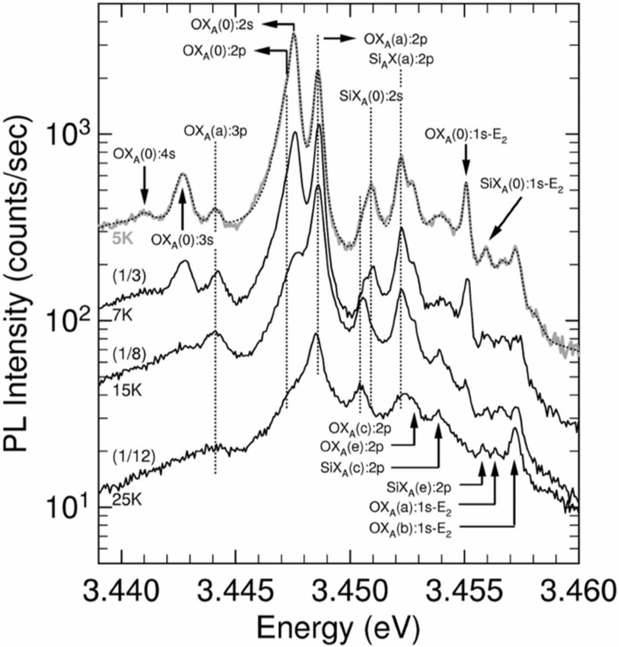
Figure 4. Spectra of Sample #2 (FS-HVPE) acquired at 2ES spectral region, measured at 5 (top spectrum), 7, 15, and 25K (bottom spectrum). The dotted line overlapping the 5K spectrum represents our best fit. The number in the bracket at the left side of each spectrum indicates the multiplication factor used to minimize spectral overlapping. Note the strong temperature dependence of the 2ES recombination process, after Freitas et al., Reference 24.
Table I. 1s-2s and 1s-2p transition energies. Note the excellent agreement between IR and PL data when taking the bound exciton excited states (BXes.) in consideration. Assuming that the separation between the 2s and 2p transition is only about 0.125 meV(*) we are not able to distinguish them experimentally.
| Transition | IR (meV) | PL (meV) (no BXes.) | PL (meV) (BXes.) |
|---|---|---|---|
| O: 1s-2s | - | - | 25.4 |
| O: 1s-2p | 25.9 | 23.3 | 25.7 |
| Si: 1s-2s | - | - | 22.8* |
| Si: 1s-2p | 22.8 | 20.6 | 22.8* |
To confirm our assignments of the emission bands associated with the pervasive donors in GaN films we carried out PL and SIMS measurements on UID and Si-doped GaN films deposited by MBE and OMCVD, respectively, on FS-HVPE GaN substrates.29 The substrates for homoepeitaxial deposition were selected from the same original piece used for FTIR, PL, and SIMS measurements. The results presented in Figure 5, show three major peaks in the spectral range between 3.441 and 3.484 eV for two homoepitaxial films along with the FS-HVPE GaN (Sample #3) spectra. The chemical nature of the impurities in the FS-HVPE GaN, has been previously discussed.16 The PL spectral range covers the region associated with recombination processes associated with the annihilation of free-excitons (FE), the dominant exciton bound to shallow neutral donor impurities (DoX), and the 2ES. Sample #3 (reference sample FS-HVPE GaN) shows two dominant peaks at ∼3.4714 eV and 3.4723 eV, which have been previously assigned to excitons bound to O and Si shallow donor impurities, respectively.24 The spectrum of Sample #2 shows one dominant peak at 3.4717 eV, which is very close to the peak attributed to neutral O donor bound exciton in the reference Sample #3. This observation is consistent with the SIMS oxygen concentration of 3.3 × 1016 cm−3 and detection limit concentration for silicon.30 The spectrum of Sample #1, the Si doped OMCVD epitaxial film with SIMS concentration of 1.5 × 1017 cm−3, is dominated by a relatively broader emission band, whose peak aligns quite well with that assigned to excitons bound to neutral Si donors at 3.4723 eV. This spectrum also shown a sharp doublet near 3.467 eV, represented by XAo, previously associated to excitons bound to an unknown shallow acceptor, which later has been identified as Mg.31,32 Note that the lines assigned to the O donor observed in the 2ES spectrum of Sample #2 dominate this spectral region, while those lines assigned to the Si donor have completely vanished, consistent with the low level of neutral Si donors.
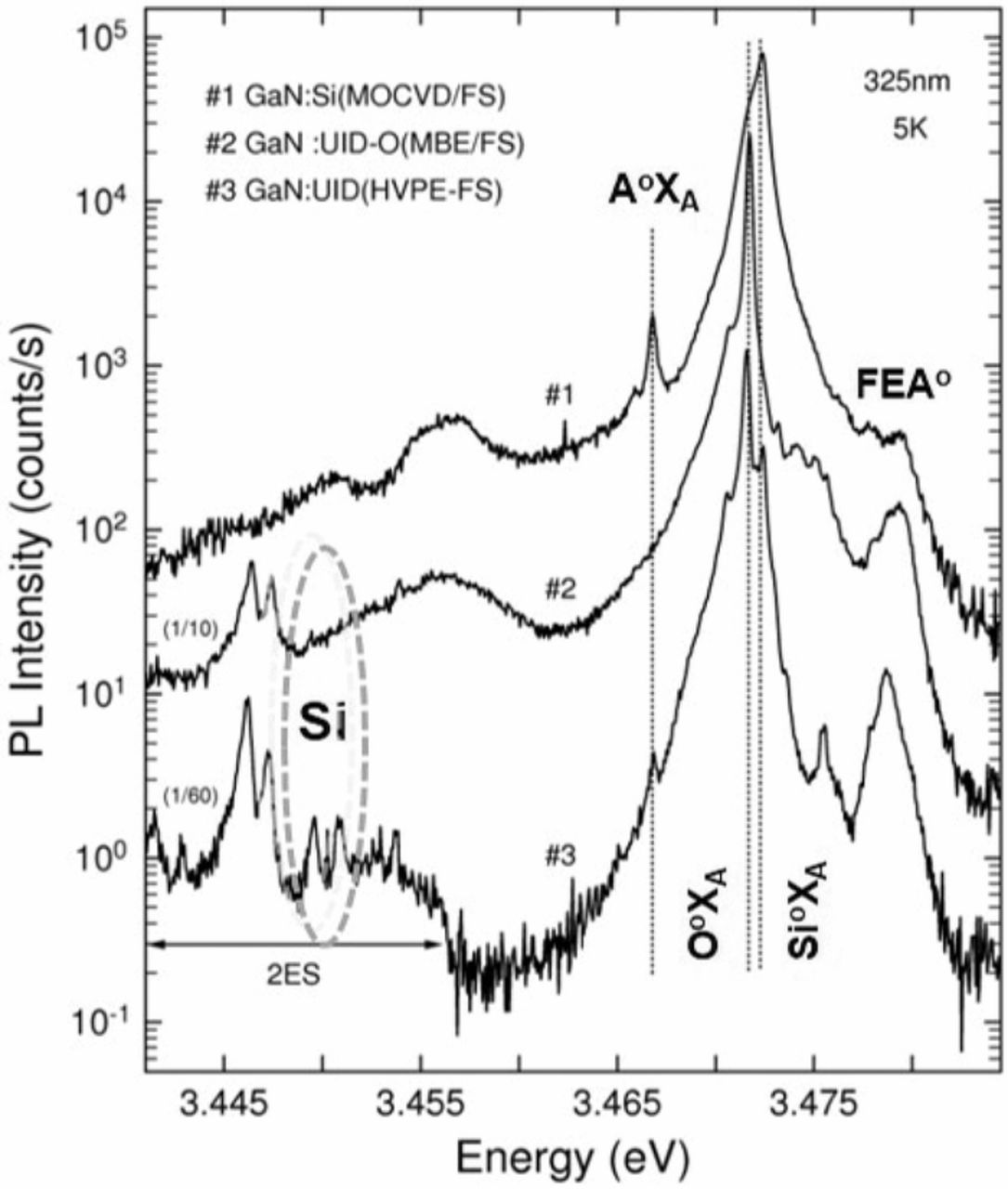
Figure 5. Low-temperature PL spectra of S#1 (Si-doped, MOCVD), S#2 (UID, MBE), and S#3 (UID, FS-HVPE) samples. After Freitas et al., Reference 29.
The results obtained from IR, PL, and SIMS experiments clearly confirm that the proposed identification and binding energies of Si and O, the two dominant pervasive shallow donors in GaN, are correct. Therefore, PL spectroscopy, which can be easily set up, can be conveniently used to detect and identify the incorporation and activation of silicon and oxygen impurities in GaN. In fact, we have recently used this knowledge to investigate the incorporation of Si and O in thick FS GaN films deposited by HVPE on HVPE-GaN/ammonothermal-GaN templates. These thick freestanding films have close to perfect crystallinity, with more than two orders of magnitude reduced free carrier concentration relative to the ammonothermal bulk GaN substrate.33 These thick films show uniform optical and electronic properties across the interface and growth surface regions, as measured by Raman scattering, PL, and SIMS, but show 10 fold increase of Si impurity concentration as the growth proceeds.34 Despite that, the room temperature mobility is over 800 cm2 /Vsec, and the FWHM of the bound exciton lines at 3.4716 eV (OoXA1) and 3.4724 eV (SioXA1) are only 146.4 μeV and 185.0 μeV, respectively, is depicted in Figure 6. These smaller FWHM were acquired for the N-polar face of the sample, which has 2.0 × 10¹⁶ Si/cm−3 (10 times less than the Ga-polar face), indicating that increasing shallow impurity concentration introduces line broadenings of both, the donor FTIR excitation spectra and the exciton PL spectra.35 These considerably smaller FWHM observed in the N-polar face (more than 50%) in comparison to that observed in the FTIR HVPE sample, which has similar concentrations of O and Si, indicates a considerable reduction of the inhomogeneous broadening typical for heteroepitaxial FS HVPE GaN films.36 Recently, Fujikura and co-workers propose a new approach to reduce the undesirable incorporation of pervasive shallow donor in HVPE GaN films, which will allow the realization of new kinds of electronic devices.9
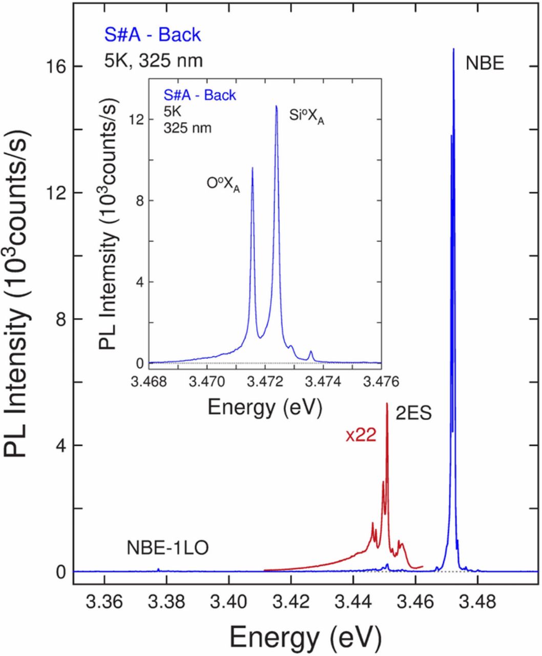
Figure 6. Low temperature, high-resolution PL spectra of the N-polar face of a FS HVPE GaN sample deposited on HVPE-GaN/Amomo-GaN template. The insert attests the sharpness of the bound exciton emission lines, and confirms the high crystalline quality of this sample. After Freitas et al., Reference 35.
Summary
This manuscript present a brief survey of the work carried out at the Naval Research Laboratory to identify the pervasive shallow donors in GaN deposited on a number of substrates by various deposition methods, and to measure their binding energies. High-sensitive SIMS depth profile measurements were carried out in previously selected unintentionally doped and doped GaN films to detect, identify, and quantify the concertation of potential shallow donors in the films. High-resolution Fourier Transform Infrared spectroscopy, a quantitative technique but not capable to identify chemical species, was employed in combination with SIMS to unambiguously identify Si and O shallow donors and yielded their ground state binding energies. High-resolution, variable-temperature photoluminescence studies of recombination processes associated with excitons bound to donors leaving the donors in their ground states and their excited states after exciton annihilation were carefully correlated with the FTIR measurements. The PL results were in excellent agreement with the energies of donor intra-impurity transitions measured by infrared absorption. High resolution PL studies of unintentionally doped and doped GaN samples clarified some conflicting aspects of Si and O donor identification and their binding energies. These studies provided the experimental foundation for the detection and identification of pervasive shallow donors in GaN grown by various methods, which have been successfully used to investigate the unintentional incorporation of Si and O in thick FS homoepeitaxial HVPE GaN films.
Acknowledgments
The work was supported the Office of the Naval Research.
ORCID
Jaime A. Freitas, Jr. 0000-0001-6662-9109