
Abstract
Fabrication of deep microchannels by a simple electrochemical discharge based multi-pass micromilling technique is reported. The effect of electrolyte concentration, tool feed rate, number of passes, and power supply on the geometric characteristics of the microchannel is presented. Numerical analysis was performed to predict the shapes and sizes of the microchannels, which matched quite well with the experimental values. An increment in the channel depth was observed with an increase in the machining voltage and the total number of passes. Through-channels were etched in a 400 μm thick glass substrate at machining voltages of 55 V and 60 V after the 6th and 5th pass respectively using a 10% KOH electrolyte. For deeper microchannels (>500μm), a higher electrolyte concentration, i.e., 30% was required, that had enhanced chemical etching, resulting in higher depth and relatively smooth channel surface. Microchannels having depth >1100 μm was obtained with a 30% KOH electrolyte concentration after the 16th pass. The number of passes required to achieve higher channel depth depends on the combined effect of voltage and the electrolyte concentration. The tool wear rate was higher at higher machining voltages. Moderate machining voltage, pulse frequency, and higher concentration are recommended for deep glass micromachining applications.
Export citation and abstract BibTeX RIS
With the development in the micromachining techniques, creating microchannels and through-holes in non-conductive transparent materials such as glass, fused silica and quartz etc., has become very important especially in radio-frequency (RF) MEMS packaging, lab-on-a-chip, micro-total-analysis-systems (μTAS), three-dimensional (3D) interconnects, biomedical and microfluidic devices, Although the microchannels in other materials such as silicon, polydimethylsiloxane (PDMS), poly(methyl methacrylate) (PMMA), etc. have been already demonstrated in microelectromechanical systems (MEMS); these materials have certain limitations. Silicon is optically opaque and semiconductor in nature, due to which it has an electrical loss while transmitting signals in high frequency. PDMS and PMMA face challenges with respect to their thermal and chemical stability.1 Directly fabrication of microfeatures in these polymer materials is not possible and thus, requires mold transfer technology. On the other hand, a glass substrate is optically transparent, chemically inert, biocompatible, and can withstand higher temperatures. Therefore, it is an excellent substrate choice for RF MEMS and microfluidic devices.
In spite of their advantages, micromachining of the glass-based materials has remained a challenging task, which is due to their fragile and hard nature. Although high aspect ratio (>100) microfeatures were fabricated in silicon substrate using HF-based electrochemical etching2,3 and by the SF6 based plasma etching method,4 creating high aspect ratio features in glass based materials is still very challenging. Wet etching, as well as plasma-based dry etching, has been used to create microfeatures in glass; however, these methods have a lower etching rate. Wet etching has isotropic etching characteristics due to which the creation of high aspect ratio features is quite challenging. The plasma etching method used to etch glass based materials has a relatively slower etch rate (<3 μm/min) and require metal-based hard mask materials such as electrodeposited nickel, gold, etc.5,6
Contact-based machining methods such as ultrasonic machining and abrasives jet machining can be used; however, tool erosion, chocking of the nozzle, lower machining rate, poor surface quality, etc., have remained the challenging tasks.7 Laser ablation, electron beam machining, focused ion beam require expensive infrastructure and have limited applications.
In this regard, electrochemical discharge machining (ECDM) has emerged as an economical and faster method to fabricate the microfeatures in glass, fused silica, and a quartz substrate. ECDM is a hybrid of electrochemical machining (ECM) and electro-discharge machining (EDM). But unlike ECM and EDM, which are used to etch conductive materials only; ECDM can be used to machine non-conductive materials. In ECM and EDM process, the material removal occurs by anodic dissolution and thermal melting and vaporization respectively;8–11 while in the ECDM process, electrochemical discharge occurs by ionizing a thin hydrogen film that surrounds the tool electrode that acts as a cathode. Due to the discharge, the temperature rises in the machining zone, and the material is removed from the non-conductive substrate, which is kept in the close vicinity of the tool electrode. Material removal is due to the combined effect of high-temperature melting and vaporization, followed by the temperature assisted chemical etching.12
Fabrication of microchannels using the ECDM process has been sparsely reported in the published pieces of literature. The layer by layer etching method was demonstrated to create 3D microstructures in the glass substrate by Zheng et al.7 Ziki et al.13 reported that the smaller tool feed rates (< 5 μm/s) resulted in microchannels with uniform surface texture and smooth sidewalls as compared to the higher feed rates (>10 μm/s). Didar et al.14 reported that the higher values of discharge voltage and the lower tool feed rates resulted in deeper microchannels. Hajian et al.15 reported a good agreement between their predicted channel depth and experimental channel depth during a single pass ECD milling process. Hajian et al.16 studied the effect of the upward magnetic field during the microchannels formation using the ECDM method and reported an improvement in the surface quality and the depth of the microchannel. Deep microchannels up to 100 μm were fabricated in a single step by Wüthrich et al.17 on a Pyrex glass wafer. Han et al.18 obtained a channel depth of 300 μm using a textured tool electrode during a single step the ECDM process. High aspect ratio microholes fabrication was demonstrated by Jui et al.19
All the earlier reported works are limited to the fabrication of shallow microchannels having depths <400 μm; however; the microfluidics and RF MEMS devices often require deeper (>500 μm) microfeatures. Hence, in the present work, deep microchannels having depth varying from 400 μm to 1100 μm were fabricated in the glass substrates by using a multi-pass micromilling technique (see Figure 4) at a tool feed rate of 50 μm/s. Such deep microchannels at high feed rate have not been reported in the literature. This work also reports the effect of electrolyte concentration on the creation of deep microchannels. It was observed that at the lower electrolyte concentration, i.e., 10% KOH, the fabrication of deep microchannels (>500 μm) is relatively challenging due to excessive tool wear and reduced material removal at higher depths. However, the higher electrolyte concentration (30% KOH), helps in increasing the etch rate, thus, through microchannels in an 1100 μm thick glass substrate were fabricated after a total number of 16 passes. The obtained experimental channel depths were validated with a FEM-based simulation model and were found in good agreement. In the present work, a low cost stainless steel material was used as tool electrode instead of conventionally used tungsten or tungsten carbide tools which are comparatively expensive. Compared to the conventional plate type counter-electrode, a ring type electrode was used, which provides a uniform electric field distribution and results in better microchannels.
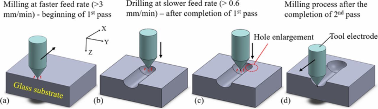
Figure 4. Schematic of multi-pass micromilling approach.
Numerical Modeling of Multiple Through-Holes Formations
The ECDM process involves a lot of complex phenomena, and hence, modeling such complex physics is challenging. Therefore, a thermal-based numerical model was build up and used to predict the depths of the microchannels. These simulated depths were compared with the experiments results obtained after the multiple micromilling passes. The number of passes indicates that number of times the tool electrode was moved along the microchannel length, i.e., the forward and backward motion. To simplify the thermal modeling of the ECDM process, the following assumptions were taken into consideration:
- (a)Material properties are homogeneous, isotropic, and temperature independent.
- (b)All the electrochemical discharges are identical and follow a normal heat flux distribution.
- (c)Since the glass substrate is surrounded by the electrolyte, only a fraction of the total heat generated termed as partition energy (Fp) is transferred into the glass.
- (d)All the glass substrate region having the temperature higher than the melting temperature (Tm), i.e., 1673 K, is completely removed.
A time-dependent 3D heat conduction differential Eq. 1 was solved to determine the temperature distribution within the glass substrate domain.
![Equation ([1])](https://content.cld.iop.org/journals/2162-8777/8/6/P322/revision1/d0001.gif)
Where k, ρ, cp are the thermal conductivity, density, and specific heat of the glass substrate taken as 1.6 W/m-K, 2170 kg/m3, 670 J/kg-K, respectively.12,20 At the start of the simulation, the temperature of the entire substrate was kept at the room temperature. Heat flux qs and convective heat loss boundary conditions were applied on one of the surfaces, while the remaining surfaces were thermally insulated.
![Equation ([2])](https://content.cld.iop.org/journals/2162-8777/8/6/P322/revision1/d0002.gif)
Where Rs is the spark radius (= 150 μm), f is the tool feed rate (= 50 μm/s), t is the simulation time, H is the convective heat transfer coefficient (10000 W/m2-K), V is machining voltage, and I is the mean current with the KOH electrolyte. It has been reported by Kulkarni et al.,11 that 77 – 96% of the input thermal energy provided at the machining zone, is carried away by the electrolyte and utilized for increasing the electrolyte temperature. Only the remaining 2–6% energy goes into the workpiece. This fraction of energy is termed as 'Partition energy'. Based on these findings a partition energy of 5% in the present study.
The spark zone was fine-meshed with a mesh size <10 μm, as shown in Figure 1a. The simulation was carried out using a uniformly moving Gaussian heat flux along the x-direction, and the temperature distribution within the substrate was obtained (Figure 1b). The maximum temperature reaches beyond 6000 K at a machining voltage of 60 V.
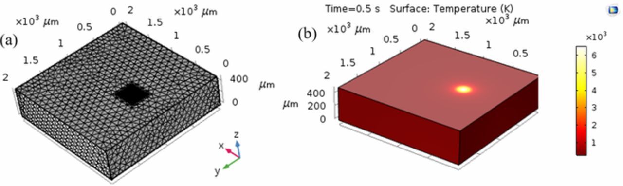
Figure 1. Images showing: (a) Refined mesh in the spark zone; (b) Temperature contour with 10% KOH at 60 V machining voltage, 70% Duty cycle, and 10 kHz frequency, 1st pass.
In the present numerical model, the chemical etching contribution in material removal is ignored. The material removal was considered due to the localized melting and vaporization only, i.e., the material was removed only from those regions where the temperature is higher than the melting point. Figure 2 shows the variation in the surface temperature along with the depth of the microchannel and radial direction (y-axis) from the spark center in the first pass. The simulated results obtained at a machining voltage of 60 V, 10% KOH electrolyte, 70% duty cycle, and 10 kHz pulse frequency showed that the average microchannel depth was approximately 100 μm.
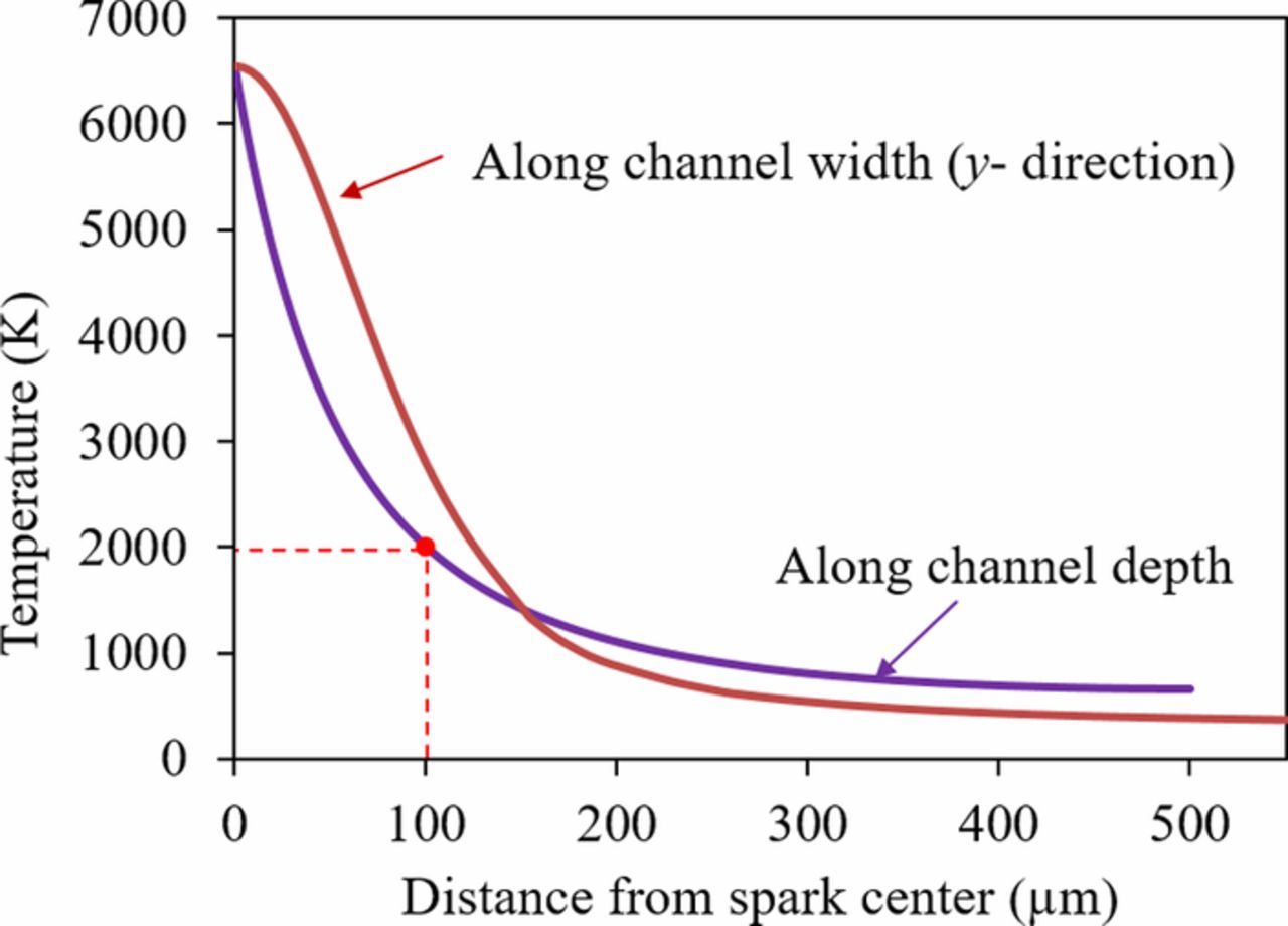
Figure 2. Graph showing the temperature variation along depth and radial direction with 10% KOH at 60 V machining voltage, 70% Duty cycle, and 10 kHz frequency obtained after the 1st pass.
Experimental
Experimental set-up
All the microchannel etching experiments were conducted in an in-house developed ECDM experimental set-up. The setup primarily consists of a computer numerical control (CNC) controlled X, Y, Z stage, a high voltage pulse power supply, an acrylic electrolyte tank, and an electrolyte circulation system. The initial tool immersion depth of 1.5 mm was maintained for all the experiments.
A commercially available high carbon steel rod was used as a tool electrode while a circular shaped stainless steel ring was used as a counter electrode. The tool electrodes had variability in their tip sizes. To measure this variability, the tip diameter of the twenty-seven tool electrodes was measured and plotted in Figure 3. Some tool electrodes had sharp and pointed tips (Figure 3b); while others were blunt (Figure 3c). Only the sharp tool electrodes were used in the experiments. However, even the sharp tools had tip diameters ranging from 60 μm to 94 μm with a sample standard deviation of 10 μm. This non-uniform size of tool electrodes affected the ECDM process and caused some variation in the microchannel profiles, i.e., depth, width, and surface quality. To reduce the effect of variability in the tool tips on the microchannels profiles, further experiments were performed by randomly selecting a tool from the set of tool electrodes. Each experiment mentioned in Table I was carried out for three times. The depth of a particular microchannel was measured by considering ten distinct cross-sections in the middle portion (to ignore the end effects) of the microchannel. The mean value for three such microchannels depth at a particular process parameter setting was considered as the channel depth at that parameter setting.
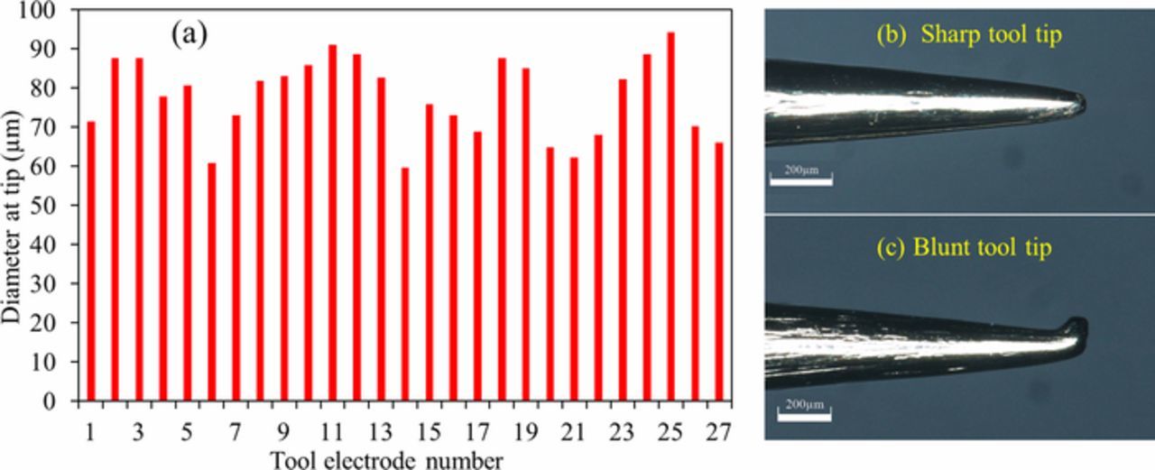
Figure 3. (a) Variation in the tool tip diameter; (b) Optical images showing sharp tool tip; (c) Blunt tool tip.
Table I. Details of ECDM process parameters used in deep microchannel fabrication.
| Process parameters | Values |
|---|---|
| Voltage | 45 V, 50 V, 55 V and 60 V |
| Electrolyte | 10%(wt) KOH |
| Tool feed rate: | 50 μm/s |
| Frequency | 10 kHz (for pulse supply) |
| Duty cycle | 70% |
| Number of passes | 3 (for DC power supply) and 6 (for pulse supply) |
Design of multi-pass ECDM milling experiments
There are two approaches to fabricate deep microchannels using the ECDM based micromilling. The first one is to perform drilling operations in Z-axis up to reach the required depth and then carry out a milling operation in the X-Y plane. In this case, the tool feed rate in the X-Y plane is lower (< 3 μm/s) due to the increased surface area, which leads to the reduced current density and thus, reduced material removal rate and higher machining time. In case, a higher tool feed rate is given, there is a risk of collision between the tool electrode and the glass substrate, resulting in possible damage to the substrate. To increase the machining rate without taking any risks, a multi-pass micromilling approach is used in this work. This approach has a high tool feed rate of >50 μm/s, lowers machining duration, and reduced tool wear.
There are several parameters that affect the microchannel formation by ECD milling process; however, in this work effect of type of power supply, machining voltage, electrolyte concentration and tool feed rate on the multi-pass channel depth during ECD milling at a constant high tool feed rate of 50 μm/s, is presented. The drilling depth for each subsequent passes was determined from average channel depth obtained at ten distinct cross-sections obtained from the previous pass. Glass substrate having a dimension of 25 mm × 20 mm × 0.4 mm was used as a work-piece. Microchannels were fabricated on the substrates in aqueous solution KOH electrolyte having a 10% concentration by weight. A constant frequency of 10 kHz and a duty cycle of 70% were maintained for the pulse power supply. Experiments were carried out using both DC and pulse power supply with process parameters values, as shown in Table I.
Figure 4 shows the important process steps involved in the fabrication of microchannel by a multi-pass micromilling technique. For the first pass, an initial gap of 20 μm was maintained between the tool electrode and the glass substrate. Once the electrochemical discharge was established at the set machining voltage, a constant tool feed rate of 50 μm/s was given to the tool electrode along the X-axis to create a microchannel as shown in Figure 4a. For the second pass, the tool electrode was given a vertical downward feed along the Z direction (Figure 4c) for a depth determined from the average depth of the microchannel cross-section obtained from the first pass. Due to this drilling process, the dimension at the end of the microchannels increases resulting in a larger overcut. A similar approach was repeated for the remaining passes to deep microchannels in the glass substrate.
Initially, the relationship between the machining voltage and the current characteristics was analyzed for all the KOH electrolyte having different concentrations. The threshold discharge voltage for 10%, 20%, and 30% KOH electrolytes was measured to be 38 V, 32 V, 28 V, respectively. When the experiments were carried out at a DC voltage of 60 V and 10% KOH electrolyte, a significant tool wear was observed due to the continuous thermal discharge. In a continuous DC power supply, there is no pulse-off period and therefore, no cooling action was taking place. As the material wear rate increases with the temperature, significant tool wear was observed.
Consequently, the gap between tool electrode and the glass substrate increased and the discharge energy was insufficient to cause any material removal. At a machining voltage of 40 V, the discharge energy was relatively low as the effective voltage was only 2 V (40V-38V = 2V), therefore the glass etching rate was very low. Hence, further experiments were performed at a machining voltage of 45 V, 50 V, and 55 V. With 10% KOH electrolyte and pulse power supply, the material removal was very small and inconsistent at a machining voltage 45 V. At a machining voltage of 65 V cracks were formed on machined microchannels due to aggressive discharge and high thermal energy. So, all the further experiments were performed within the range of 50 V, 55 V, and 60 V.
Up to three passes were performed to fabricate the microchannels using a DC power supply. As the pass number was increased >3, tool wear was quite significant with the DC power supply at machining voltage >50 V. This is due to the combined effect of continuous thermal energy supplied with DC power supply and decrease in the electrolyte supply and heat dissipation as the channel depth increases. However, with the pulse power supply, comparatively lesser tool wear was observed due to the cooling action of the electrolyte during the pulse-off time. Therefore, a large number of passes could be performed with the pulse power supply to fabricate high aspect microchannels.
Deep microchannels were fabricated using multi-pass techniques for each parameter settings with three repetitions each. After the completion of experiments, the cross-sections of the glass substrates were polished using commercially available emery papers of grit sizes ranging from 320 to 1200. The substrates were cleaned thoroughly and analyzed using an optical microscope to measure the depth and surface morphology of the microchannels.
Experimental Results and Discussion
Shallow microchannel formation by DC power supply
Figure 5 shows the microscopic images of the microchannels depths obtained in different passes at machining voltages ranging from 45 V to 55 V. It can be observed that the channel depth increases with an increase in the pass number and the machining voltages. With an increase in the machining voltage, the discharge energy increases, resulting in higher machining depths.
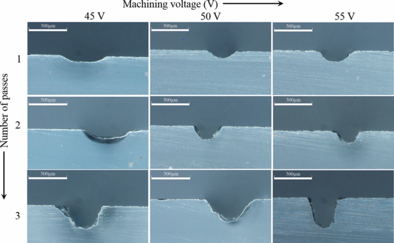
Figure 5. Depths of microchannels obtained with DC power supply at different machining voltages during multi-pass ECD milling.
Figure 6 shows the comparison of the numerical and the experimental microchannel depth with the pass number at different machining voltages. The simulated channel depth shows a matching trend with the experimental values for all the passes. The simulated channel depths values were higher than the experimental values, and the difference in the respective values increases with the increase in the number of passes. It could be due to the assumption made in the present model with respect to energy partition and flushing efficiency, which is taken a constant value for each pass. The difference in values also suggests that during experimentation, as the pass number or channel depth increases, electrolyte faces difficulty in reaching the machining zone. Consequently, the flushing efficiency and the partition energy reduce with an increase in the pass number.
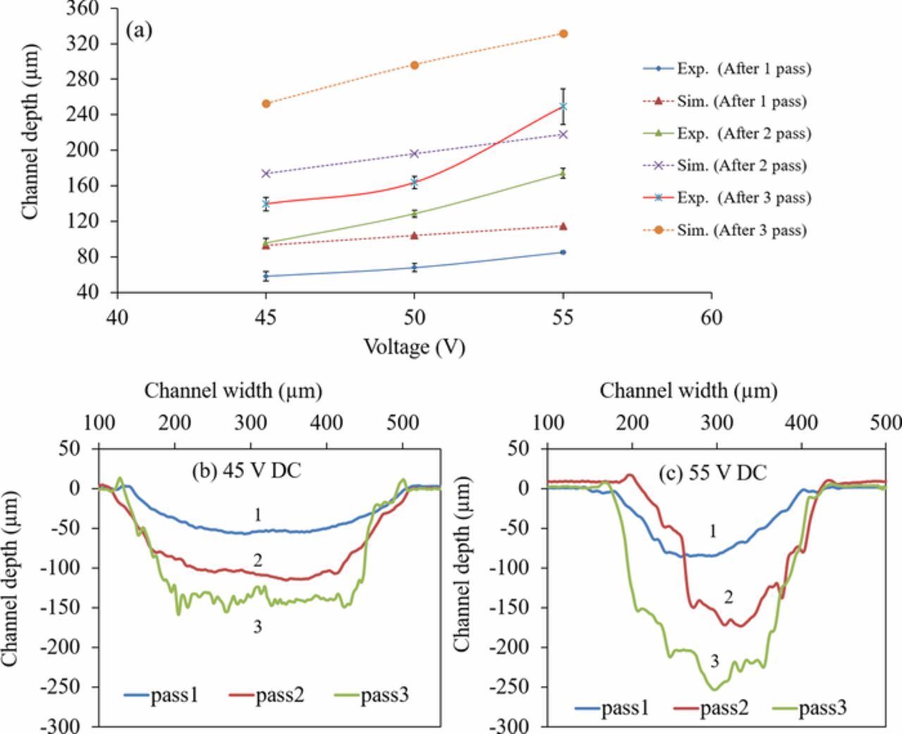
Figure 6. Multi-pass microchannel depth evaluation: (a) Numerical predicted channel depths vs. experimental channel depths. Experimental profile of the microchannel obtained after different pass with 10% KOH and 50μm/s tool feed rate (b) 45 V and; (c) 55 V machining voltage.
Figures 6b and 6c depict the experimental profile of the multi-pass microchannels obtained from the zeta optical microscope at 45 V, and 55 V respectively. The profiles were obtained by taking the mean value of ten different cross-sections profiles of a particular microchannel. It can be seen from these images that the profiles of microchannels were close to the isotropic nature, and the depths are not uniform.
Shallow microchannel formation by the pulse power supply
As the tool wear was relatively large in the case of DC power supply, experiments were performed with the pulse power supply to study the effect of machining voltage on channel depth. Figure 7 shows the depth of the microchannels obtained with different machining voltage and the pass number. The depth of the microchannels increases with an increase in the machining voltage. A similar trend, i.e., rise in the channel depth is also observed when the pass number was increased.
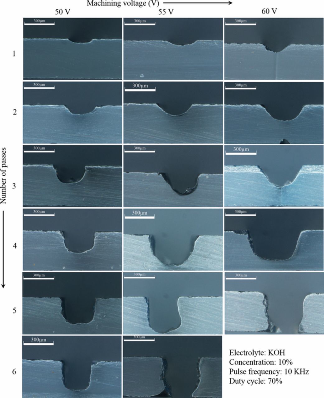
Figure 7. Cross-sectional images of the microchannels machined in glass substrate at varying machining voltages and passes.
Figure 8 shows the variation in the depths of microchannel predicted by the numerical simulation and that obtained with the multi-pass experiments. The predicted microchannel depths were greater than the experimental values. Moreover, the difference in values increases with an increase in the number of passes. During the experiments, the circulation of electrolyte becomes difficult in reaching the discharge zone, especially as the depths increase. Consequently, the flushing efficiency and the partition energy reduce with an increase in the machining depth.

Figure 8. (a) Comparison of experimental and numerical microchannel depths at 70% duty cycle, 10 kHz frequency and 10%KOH electrolyte. Experimental profile of the microchannel obtained after different passes at (b) 50 V; (c) 60 V. Tool feed rate was kept at 50μm/s.
Figures 8b and 8c show the experimental profile of the microchannels etched at machining voltages of 50 V, and 60 V respectively. The depth profiles are obtained by taking the mean value of ten different cross-sections profiles of a particular microchannel. It can be seen from these images that depths of microchannels increase with an increase in the machining voltage and the number of passes.
Figure 9 shows the isometric view of the through microchannels obtained in the sixth and fifth pass at a machining voltage of 55 V and 60 V, respectively. At higher machining voltage, comparatively deeper channels were created in each pass due to higher discharge energy and material removal rate, and therefore, a lesser number of the pass was needed to create a through-channel.
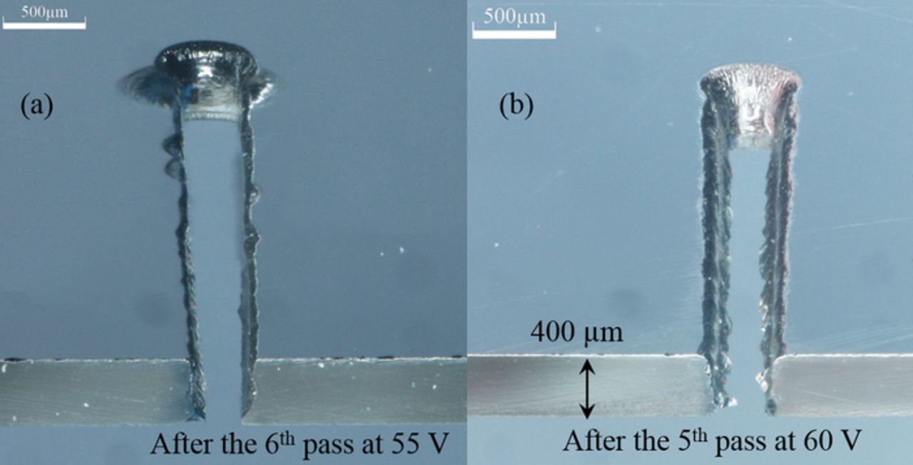
Figure 9. Isometric view of the through microchannels obtained with 10% KOH electrolyte: (a) After the 6th pass at 55 V; (b) After the 5th pass at 60 V.
Figure 10 shows the microchannel fabricated after the fifth pass using 10% KOH electrolyte at 60 V machining voltage. From Figure 10b, it can be observed that the end of the channel had a relatively larger overcut compared to the average channel width. It is because the tool electrode was given a vertical feed after each pass during the drilling step of the multi-pass approach. Thus, the channel ends were exposed to a more significant number of electrochemical discharges compared to other parts of the microchannels. As a result, the ends of the microchannel had a larger overcut.
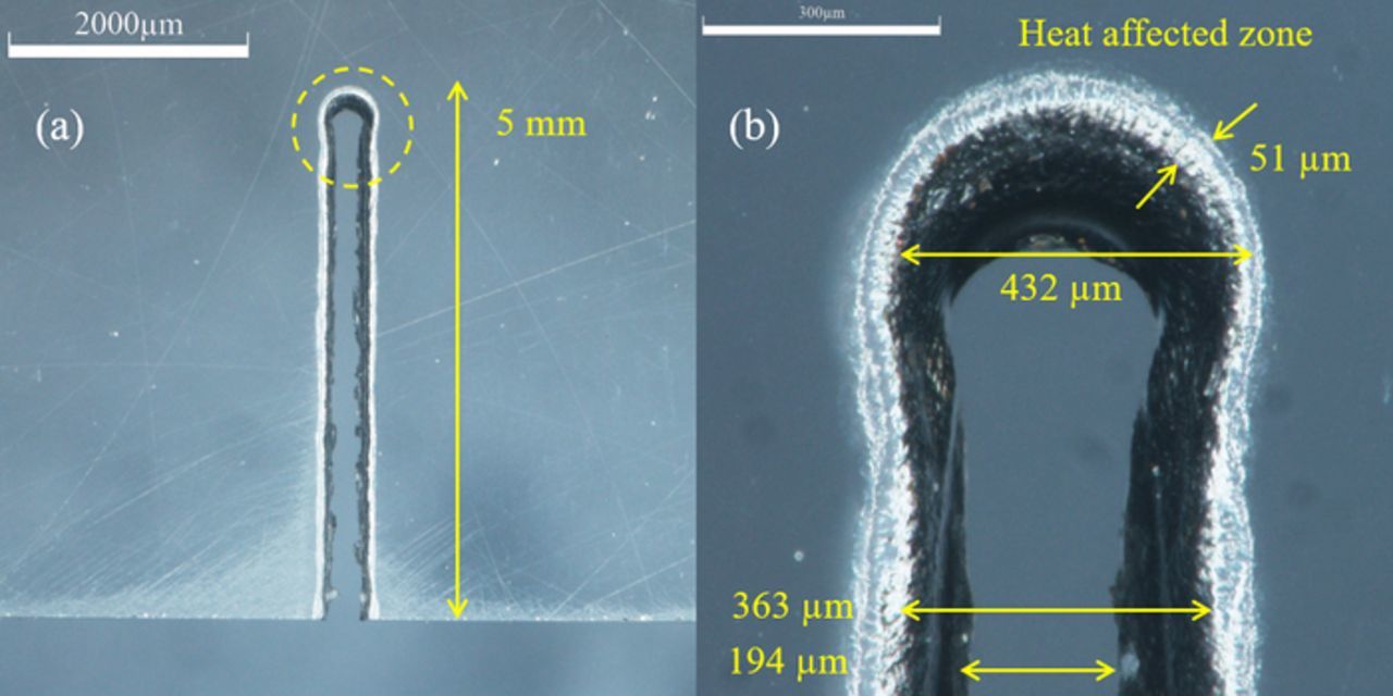
Figure 10. Optical image of microchannel obtained after the 5th pass at 60 V: (a) Through microchannel having 5mm channel length; (b) Overcut at the channel end and the heat affected zone. Constant parameters: 70% duty cycle, 10 kHz frequency and 10% KOH electrolyte.
Further, the fabricated microchannel had a tapered profile due to the larger channel width at the top surface (363 μm) compared to the width at the bottom surface (194 μm). The reduction in the channel width along the depth is due to the longer duration of electrochemical discharge at the top surface and insufficient electrolyte circulation and the lower material removal rate in the deeper channels. The fabricated microchannels also had heat affected zone area near the top surface with fine microcracks which increased with an increase in the electrolyte concentration. Due to the capillary action, the KOH electrolyte passes through the microcracks generated in the glass substrate and subsequently etch the softened glass by the chemical etching action.
A comparison between the predicted and the experimental microchannel profile is shown in Figure 11. Comparing the channel profile after the first pass, it can be observed that the predicted channel profile shows differences with the experimental one. It is due to the normal heat flux profile assumed during the simulation while, in reality, the path of the electrons is directed toward the counter electrode and heat flux distribution might not follow the ideal normal distribution.12 Also, the simulation model ignores any effect of tool wear, which can lead to an increase in the gap between the tool electrode and the substrate during actual experimentation and reduce the energy partition. Further, as the number of passes increases, the gap between the predicted and experimental channel increases suggesting insufficient flushing of the reaction products in deeper microchannels and increased re-deposition of debris. Therefore, the predicted depths of the microchannel are larger than the experimental ones.
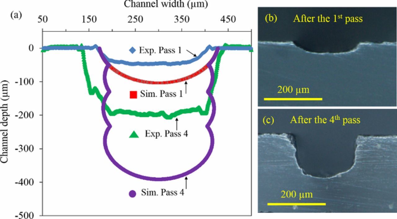
Figure 11. Comparison of numerical and experimental profiles of the microchannel obtained at 50 V machining voltage. Other parameters are: 70% duty cycle, 10 kHz frequency and 10% KOH electrolyte.
Fabrication of deeper (>500 μm) microchannels in a thick glass substrate
The detailed understanding of critical process parameters required to etch glass material obtained from the etching of shallow microchannels in a 400 μm thick glass substrate was carried forward to fabricate very deep microchannels in an 1100 μm thick glass substrates. Since the etch rate of the glass material reduces as the microchannel depth increases, a constant tool feed rate cannot be implied at the higher passes (>6) and should be reduced as the channel depth increases. This phenomenon is similar to the aspect ratio dependent etching behavior known in the plasma etching processes.21 Therefore, the microchannel etching experiments were performed by gradually reducing the tool feed rates (for higher passes). All other parameters were kept constant, i.e., 50 V as machining voltage, 10 kHz pulse frequency, and 70% duty cycle.
In the beginning, the experiments were conducted with 10% KOH electrolyte with different passes. After the 16th pass, total depth of 450 μm was achieved; however, the increase in channel depth slowed down as the passes were further increased due to the insufficient electrolyte circulation and flushing of reaction products in deeper channels having depths >300 μm.22 From the literature, it is understood that at a higher electrolyte concentration, the material removal rate increases and machining time reduces.23,24 Hence, to fabricate deep microchannels having depth >1100 μm in a shorter duration of time, further experiments were performed with an electrolyte having higher concentrations, i.e., 20% and 30%.
At higher electrolyte concentrations and passes, microcracks were observed in the heat affected zone (see Figure 12), which is the whitish region formed on the top surface on either side of the machined microchannels. These cracks were formed due to excessive thermal energy generated at higher electrolyte concentrations. However, the electrolyte may penetrate through these microcracks and help in the chemical etching of the glass substrate and enhance the material removal process.
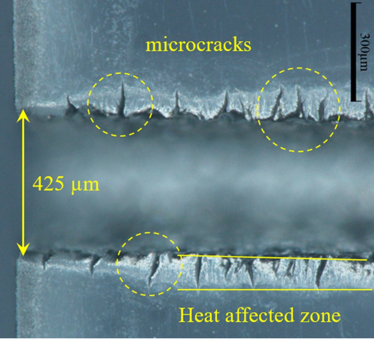
Figure 12. Optical images showing microcracks formed in the heat affected region in the microchannels obtained in the 20th pass and with the 20% KOH electrolyte.
The cross-section images of the microchannels obtained with 10%, 20%, 30% KOH electrolyte obtained in different passes are shown in Figure 13. It can be observed from the figure that the channel depth increases with a rise in the electrolyte concentration. With an increase in the electrolyte concentration, both the rate of chemical etching and the rate of electrochemical reaction increase, leading to a rise in the material removal rate and channel depth. The variation of experimental channel depth with different passes and electrolyte concentrations is shown in Figure 14. Through channels (>1100 μm) were fabricated with 30% KOH electrolyte concentration in the 16th pass compared to 680 μm channel depth obtained with 20% KOH electrolyte. Thus, the use of electrolyte having higher concentration should be used in case deeper microchannels need to be formed in shorter time durations.
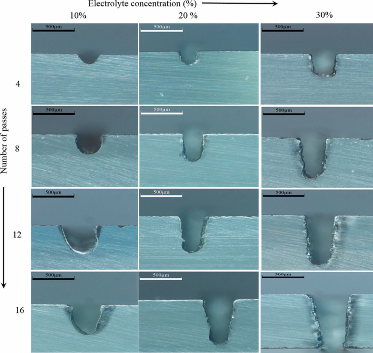
Figure 13. Cross-sectional images of microchannels obtained after varying number of passes and electrolyte concentration.
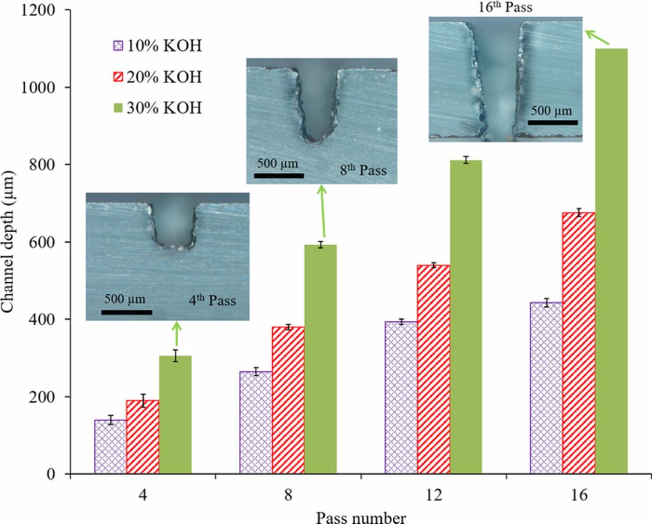
Figure 14. Variation in the microchannel depth with varying passes and electrolyte concentrations.
Figure 15 shows the 3D optical profile and the cross-section of the microchannel obtained after the 12th pass with a 30% KOH electrolyte concentration. With an increase in the depth of the channels, the taper angle of the profiles increases due to an increase in the difference between the top and bottom channel width. The channel width at the top surface is larger due to the longer exposer to the electrochemical discharges. The fabricated microchannel had a depth and width of 815 μm and 365 μm respectively, having an aspect ratio >2.
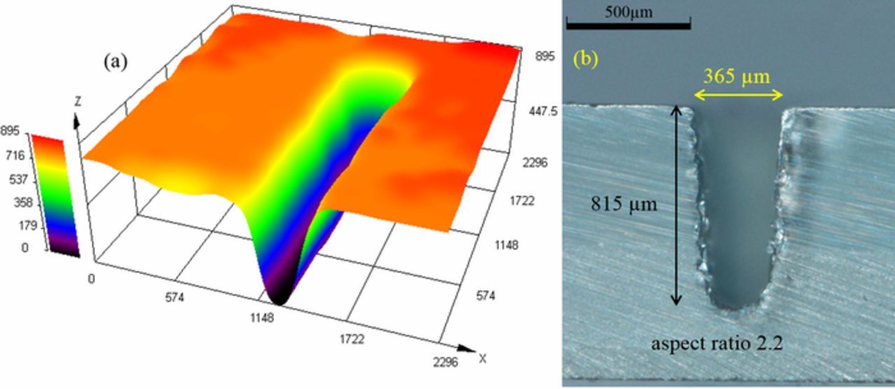
Figure 15. Optical images showing the microchannels obtained after the 12th pass with 30% KOH electrolyte: a) 3D profile; b) cross-section of microchannel.
Conclusions
High aspect ratio microchannels were formed in the glass substrate by using a simple multi-pass electrochemical discharge based micromilling method. Although both DC power, as well as the pulse power can be used; the experimental results obtained with the pulse power are better than those obtained with the DC power supply.
- Channel depth showed an increasing trend with an increase in the machining voltages both in DC power supply as well as pulse power supply. In the case of DC power supply, the tool wear rate was quite high; therefore, forming deep channels by easily available high carbon steel electrodes was challenging. Although lower machining voltages (<45V) would reduce the tool wear rate, the etch rate would also be lower, resulting in higher machining time. Pulse power supply with higher voltages (>50V) should be used to fabricate deep microchannels.
- A matching trend between the simulated and experimental results was observed. However, the numerical simulation does not consider the effect of the tool wear mechanism. Hence the simulated results have higher machining depths.
- Channel depth was measured to be increasing when electrolyte having a higher concentration was used.
- Thermal energy released during the electrical discharge creates microcracks in the glass substrate. The crack density increases from the starting section of the channel to the end section of the channel. Due to the capillary action, the electrolyte leaks through these cracks and start etching glass; therefore, by increasing the electrolyte concentration from 10% to 30%, the number of passes required to create through-channel was reduced from 36 to 16.
- Finally, the microchannels having depths varying from 400 μm to 1100 μm were fabricated by an increasing number of passes using a simple yet effective multi-pass technique. These deep microstructures have potential applications in the microfluidic and RF MEMS packaging.
Acknowledgment
The authors would like to acknowledge the financial support from the Ministry of Human Resources and Development (MHRD) and the Department of Scientific and Industrial Research (DSIR) through (DSIR/PACE/TDD-IMPRINT/7510). This work has been carried out as a part of the Impacting Research Innovation and Technology (Imprint) Project, initiated by MHRD, Government of India, under the research grant 10007457.
ORCID
Dileep Kumar Mishra 0000-0002-1846-6752
Pradeep Dixit 0000-0001-6706-1877