
Abstract
The behavior of metals penetrating the silicon substrate through a screen SiO2 or Si3N4 film by the collision of arsenic ion and surface metals are quantitatively demonstrated. We have found using silicon step etching followed by ICP-MS and SIMS that 0.1∼8% of surface metals (Fe, Cr, Ni, Cu, and W) penetrate silicon even when implanted through screen SiO2 film, depending on metal species and the film thickness. The surface metals on a CVD Si3N4 film can also penetrate into the silicon during ion implantation and/or subsequent annealing. W is most difficult to penetrate the thermally-grown SiO2 film, while W and Cr can easily penetrate a CVD Si3N4 films. We have also found using microwave photoconductive decay measurements that recombination centers are generated in silicon by low level metal penetration even when implanted through screen SiO2.
Export citation and abstract BibTeX RIS

This is an open access article distributed under the terms of the Creative Commons Attribution Non-Commercial No Derivatives 4.0 License (CC BY-NC-ND, http://creativecommons.org/licenses/by-nc-nd/4.0/), which permits non-commercial reuse, distribution, and reproduction in any medium, provided the original work is not changed in any way and is properly cited. For permission for commercial reuse, please email: oa@electrochem.org.
Metallic contamination on silicon surfaces has a detrimental impact on the performance and yield of ULSI devices. Surface metal impurities degrade the gate oxide integrity while metal impurities dissolved in silicon cause recombination centers and these result in junction leakage, degrade retention characteristics in DRAMs, and cause dark currents in image sensors. Surface metal impurities often penetrate the silicon by thermal diffusion in ULSI processing. The diffusion behavior of these metal impurities in silicon is well-known.1–3 Most metallic contamination occurs during wafer processing, particularly reactive ion etching and ion implantation4–6 and here it has been reported that metals transported with dopant ion from an ion source or acceleration tube in ion implantation equipment can be deposited on silicon surfaces.5,6 On the other hand, the behavior of surface metal impurities penetrating by the collision with a dopant ion has not been known. The ion implantation may assist surface metal impurities penetrating the screen films and silicon. The collided metal atoms' penetrating silicon can be prevented by screen films such as SiO2 or Si3N4 films,7 in which the diffusion coefficients of metal impurities such as Ni and Cu are smaller than in Si.8
In this paper, the behavior of metals penetrating the silicon substrate through a thermally grown SiO2 or CVD Si3N4 film by the collision of dopant ion and surface metals and subsequent annealing are quantitatively demonstrated. The generation of recombination centers due to the metal penetrating silicon is also discussed.
Experimental
Czochralski (CZ) Si (100), (p-type, 8–12 Ωcm), 200 mm diam. wafers were used in this study. A group of wafers was oxidized to form silicon oxides on the surface. The thickness of the silicon oxide was 5 nm, 20 nm, 80 nm, 120 nm, and 160 nm. A Si3N4 film was deposited on the surface of another group of wafers at 700°C by low pressure CVD. The thickness of the Si3N4 film was 20 nm.
Next, the silicon wafers were cleaned with NH4OH/H2O2/H2O mixture and HCl/H2O2/H2O mixture. The surfaces of the SiO2 and Si3N4 films of the wafers were hydrophilic. The silicon wafers were then quantitatively contaminated with metals (Fe, Cr, Ni, Cu, and W) by spin coating the diluted standard solutions for atomic absorption spectrometry analysis of trace metal impurities. The standard solution was composed of nitric acid solving metal (Fe, Cr, Ni, Cu, or W) and their solutions were mixed and diluted to 10 ppm by ultrapure water.9,10 The target of average metal concentration on the wafers was 2 × 10¹³ atoms/cm2 much enough to detect metals penetrating in silicon with chemical analysis and secondary ion mass spectrometry (SIMS). Fig. 1 shows an example of surface metal concentrations measured at 9 positions (x (mm), y (mm) = (0, 0), (60, 0), (60, 60), (0, 60), (−60, 60), (−60, 0), (−60, −60), (0, −60), (60, −60)) of the wafers by using total X-ray reflection fluorescence spectroscopy (TXRF) (Technos Co., Ltd, TREX 620). The in-plane deviation of the surface Fe, Cr, Ni, Cu, and W concentration were as low as 2.5%, 3.0%, 2.1%, 2.0%, and 7.5% to average concentration, respectively. The wafers were implanted with As ions at a dose of 1 × 10¹⁴ atoms/cm2 and an ion energy of 1 MeV. The annealing temperature and time were 900°C and 20 min. The amount of surface metals was measured at 9 points using TXRF before/after annealing after ion implantation. The amount of sub-surface metals in the wafers was measured using Si chemical step etching followed by inductively coupled plasma mass spectrometry (ICP-MS) (Agilent 7500 cs) and SIMS (CAMECA IMS-4FE7) after ion implantation and/or annealing. An aqueous HF/HNO3 mixture (38%HF: 68%HNO3 = 3: 100) was used for the silicon etching and metal collection.11 The etching depth per etching was 1 μm. The metals on the top surface and in the silicon oxide and silicon nitride were also collected to be quantified by the HCl/HNO3 mixture (20%HCl : 68%HNO3 = 10: 1) and dilute HF (38% HF : H2O = 1:10), respectively. In SIMS analysis, O+ ion was used for a primary ion to enhance a sensitivity of metals, while arsenic sensitivity is lower for O+ ion than for Cs+ ion. Ni was separately measured using 58Ni at high mass resolution mode in this SIMS analysis because 58Ni signal cannot be separated from 29Si while 60Ni signal cannot be separated from 28SiO2 at normal mode, resulting the background level of Ni signal is high. After the annealing, the distribution of recombination centers in the oxidized wafer induced by metal impurities was determined using recombination lifetime measurements. Silicon wafers were contaminated with ultralow level of metals as little as 2 × 10¹¹ atoms/cm2 for the measurements to detect recombination centers induced by so little metal impurities that cannot be detected by chemical analysis such as ICP-MS. Each standard solution of Fe or Ni was diluted to 0.1 ppm for individually spin coating metals as little as average 2 × 10¹¹ atoms/cm2 on the wafers. The amount of surface metals was measured at 81 points using TXRF (Technos Co., Ltd, TREX 6000 TVD)12 to obtain the in-plane distribution of the metals before/after ion implantation. The in-plane distribution of surface metals on the wafers before the ion implantation and annealing was from 1.0 × 10¹⁰ to 1.3 × 10¹² atoms/cm2 relatively larger than that of metals targeted toward 2 × 10¹³ atoms/cm2, as shown in Fig. 9a. In the recombination lifetime measurements, microwave photoconductive decay (μ-PCD) (Semilab Co. Ltd, WT-2000) was used.13 The wavelength of the incident light was 904 nm and the penetration depth was 30 μm.
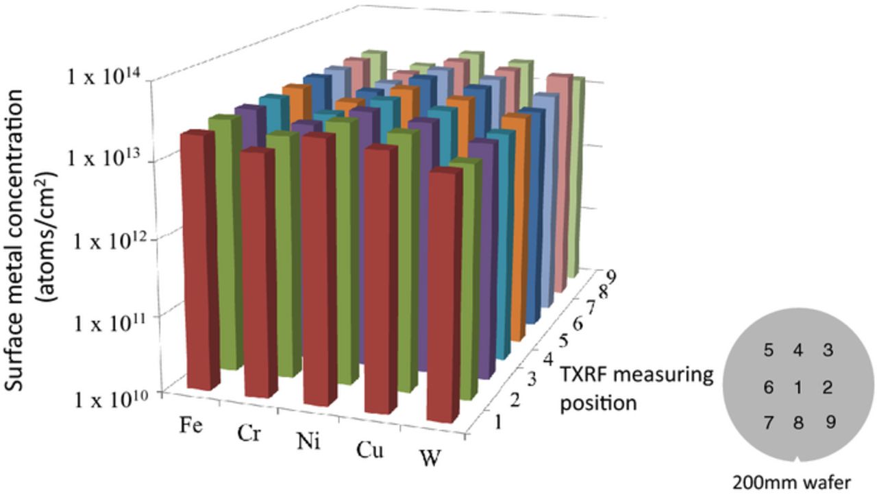
Figure 1. An example of the concentration of spin-coated metals on the hydrophilic surface of silicon wafers.
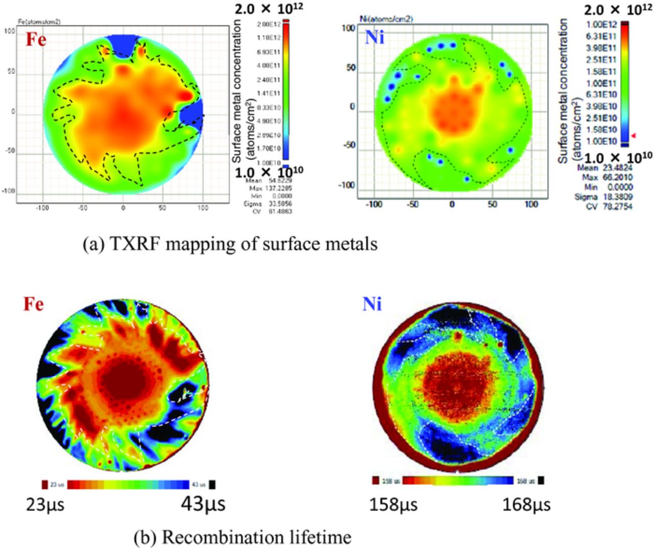
Figure 9. Fe and Ni concentration on surface before arsenic ion implantation and recombination lifetime of silicon with 20 nm SiO2 after ion implantation followed by annealing.
The diffusion barriers of Fe, Cr and Cu in high-temperature cristobalite SiO2 and β-Si3N4 were calculated by ab initio calculations.14 The thermally grown SiO2 and CVD Si3N4 films used in the experiments are not stoichiometric crystal structures,15 while supposing crystal structure must be necessary for the calculations. Thus, high-temperature cristobalite SiO2 and β-Si3N4 whose densities are known to close to those of the thermally grown SiO2 and CVD Si3N4, respectively, were used for the model. The densities of thermally grown SiO2 and CVD Si3N4 are 2.2 and 3.1, respectively.16 Those of high-temperature cristobalite SiO2 and β-Si3N4 used in the calculation are 2.3 and 3.3, respectively, close to those of the films in the experiments. The calculation method is the first principles calculation based on the density functional theory and pseudopotential. The program package used in this study is CAmbridge Serial Total Energy Package (CASTEP).17 In this method, the ground state of the system is found by solving the Kohn-Sham equation that is a rule equation of the electronic system for given atomic configuration. The wave function is expanded as plane-waves, and ultrasoft pseudopotential is used to reduce a plane-wave number. The cut off energy for the plane-wave expansion is 340 eV. The generalized gradient approximation (GGA) is adpted in the evaluation of the exchange-correlation term, and the function from suggested by Perdew et al.18 is used. The density mixing method is done for optimization of the electric system, and the Broyden Fletcher Goldfarb Shanno (BFGS) optimizing structure method is done for optimization of atoms placement. k point sampling was performed at 2 × 3 × 3 special points of a Monkhorst-Pack grid.19 In the calculation of high-temperature cristobalite SiO2, the supercell of 2 × 1 × 1 times as large as the conventional cell, in which Si 16-atoms and O 32-atoms are included, is used. The interstitial sites of the tetrahedral (T-site) and hexagonal (H-site), and substitutional site are considered as the sites for metal atoms (Fe, Cr, Cu). In the calculation of β-Si3N4, the supercell of 2 × 1 × 1 times as large as the conventional cell, in which Si 24-atoms and O 18-atoms are included, is used. The interstitial sites of the tetrahedral (T-site) and dodecagonal (C-site), and substitutional site are considered as the sites for metal atoms (Fe, Cr, Cu). In the substrate, one Si atom is replaced be one metal atom. In the kick-out mechanism, one metal atom pushed out one Si atom to T site or C-site. The most stable site of the impurity atom and the total energy of calculation cell are found by the geometry optimization. Thus, the activation energy of impurity atom in high-temperature cristobalite is obtained.
Results and Discussion
Quantification of metals penetrating silicon through screen silicon oxide
Figure 2a shows the average concentration of metallic contamination on the surface of silicon wafers before/after ion implantation. The initial concentration was 7 × 10¹³ atoms/cm2. After ion implantation, the amount of all metals on the surface was reduced 15–25%. Some of surface metals are considered to penetrate silicon and others will be sputtered and disappeared. Average surface metallic concentration of the silicon wafers before/after ion implantation followed by annealing at 950°C for 10 min is shown in Fig. 2b. The initial concentration was 2 × 10¹³ atoms/cm2. After post-implantation annealing, the amount of the metals on the surface was reduced more than that after ion implantation, particularly the amount of the surface Cu was reduced up to 99.5%. Cu will be diffused in silicon much deeper than any other metals due to the larger diffusion constant.
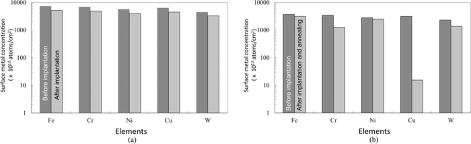
Figure 2. Average TXRF metal concentrations (a) before/after arsenic ion implantation and (b) before/after ion implantation followed by Annealing (5 nmSiO2).
Figure 3 shows sub-surface Ni concentration after ion implantation. Ni concentration of two different initial concentrations (2 × 10¹³ atoms/cm2 and 5 × 10¹² atoms/cm2) of silicon wafers is shown in the figure. The left two bars show surface Ni concentration before/after ion implantation and the right three bars shows the sub-surface Ni concentration in 1 μm each depth. Approximately 5% of the surface Ni penetrates silicon and is present at a depth of ∼1 μm. The penetrating rate of surface Ni was constant and independent of initial surface concentration. Figure 4 shows SIMS profiles of sub-surface Ni in silicon implanted through 5 nm-thick SiO2 with arsenic followed by subsequent annealing. Ni penetrates silicon through the silicon oxide to be grouped around the implanted dopant in silicon substrate. This is in agreement with the depth of Ni residing in silicon as shown in Fig. 3. Figure 5 shows SIMS profiles of sub-surface Fe, Cr, and Cu in silicon implanted with arsenic without annealing or annealed without implantation. In this experiment, the dose amount of arsenic was 1 × 10¹³ atoms/cm2. All metals penetrate silicon to a depth of ∼1 μm which is shallower than the depth of the dopant for arsenic implanted silicon without SiO2, as shown in Fig. 5a.
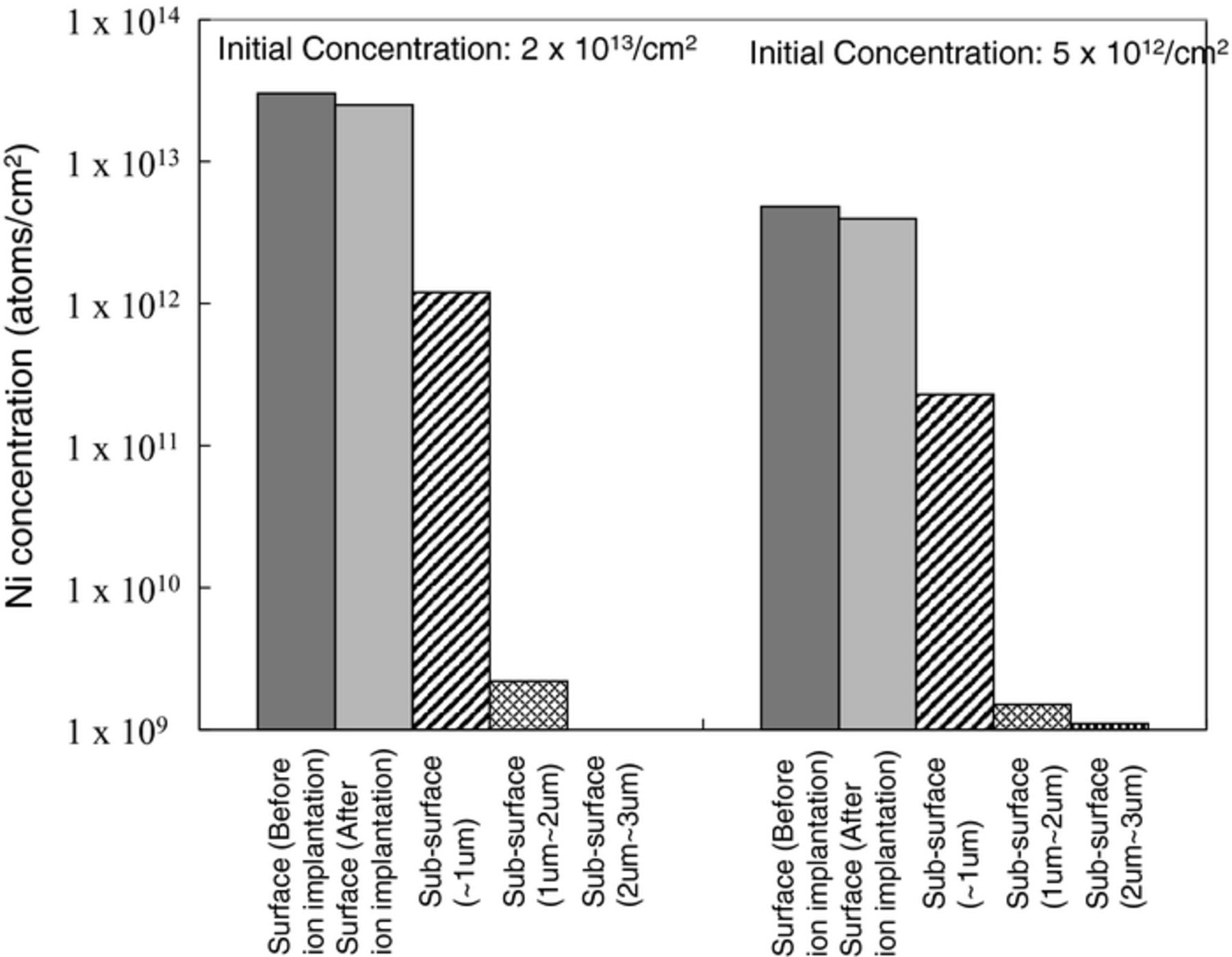
Figure 3. Sub-surface Ni concentrations after arsenic ion implantation.
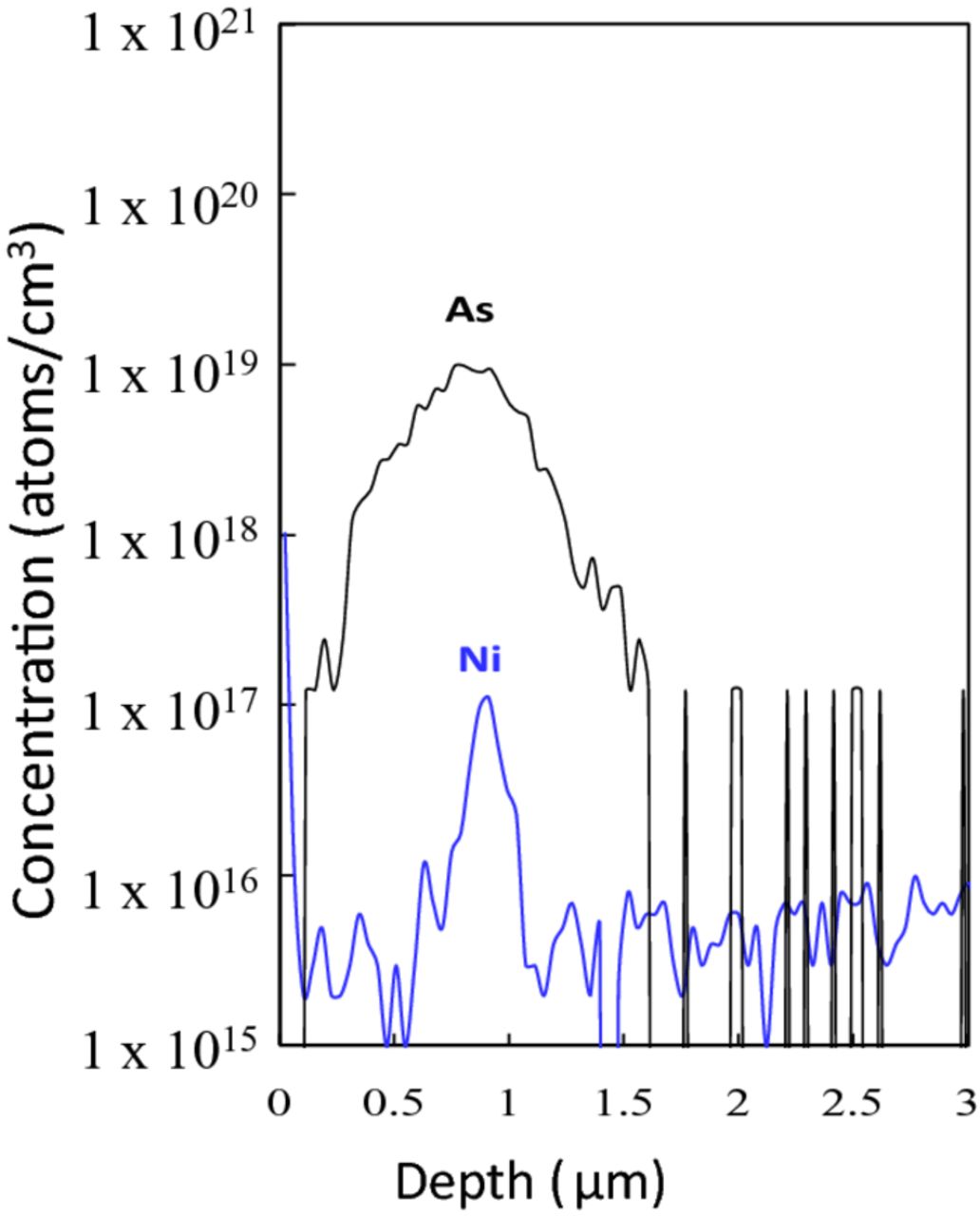
Figure 4. SIMS profiles of sub-surface Ni in silicon implanted with arsenic through screen SiO2 followed by annealing at 950°C (As dose: 1 × 10¹⁴ atoms/cm2).
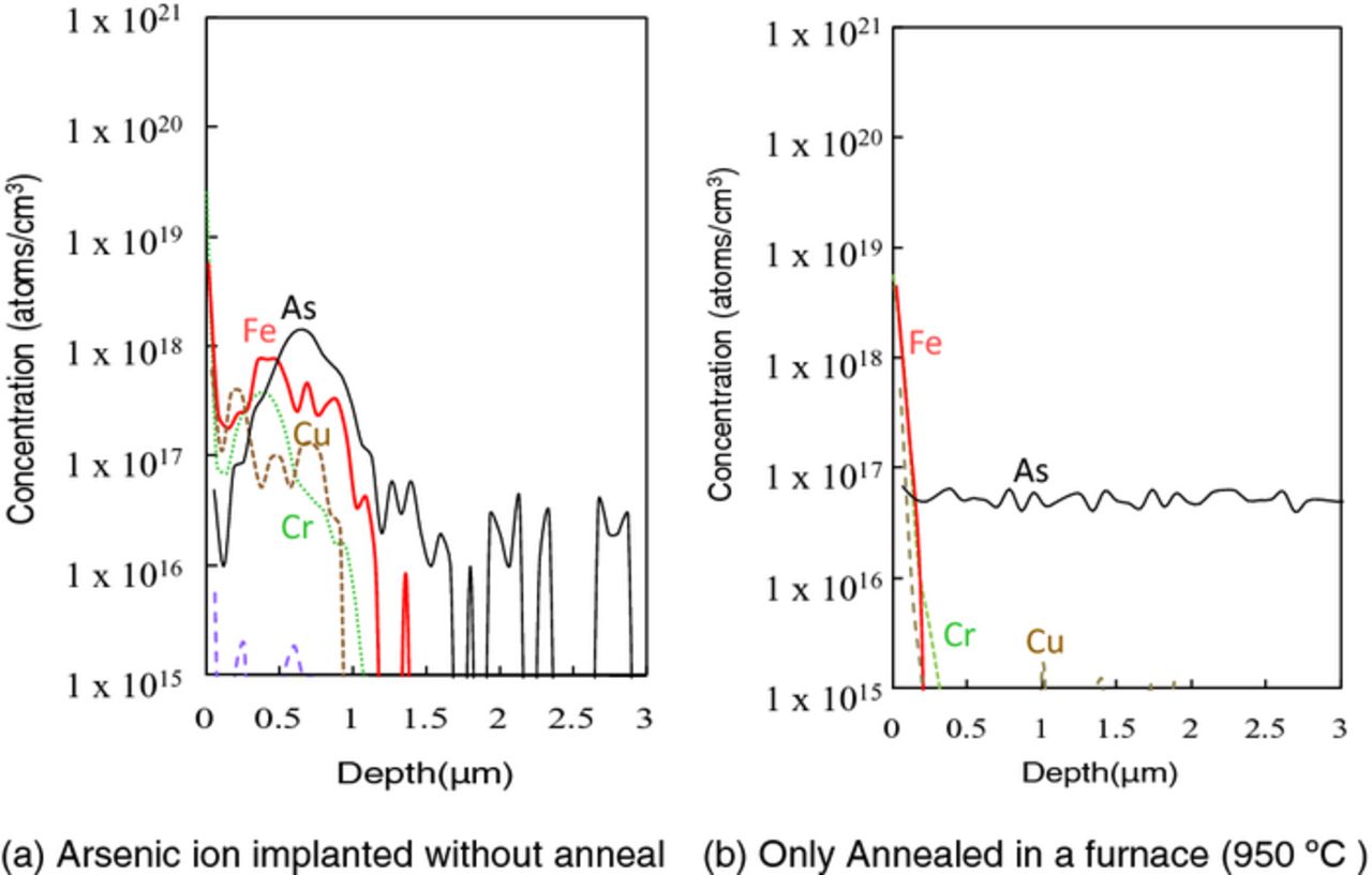
Figure 5. SIMS profiles of sub-surface metals in silicon implanted or annealed without SiO2 (As dose: 1 × 10¹³ atoms/cm2).
On the other hand, very little metals are detected in the depth of ∼3 μm in the annealed alone sample as shown in Fig. 5b. Some of surface metals are considered to be diffused in whole silicon and sub-surface concentration is attenuated. Figure 6 shows SIMS profiles of sub-surface metals in silicon implanted with arsenic through 5 nm SiO2. No metal was detected in the implanted silicon with SiO2, as shown in Fig. 6a. No metal penetrates silicon dioxide but are trapped in the silicon dioxide. As shown in Fig. 6b, after post-implantation annealing, Fe and Cu penetrate SiO2 to be grouped around the implanted dopant in silicon substrate. This behavior is the same as Ni as shown in Fig. 4. It is assumed that these metals got trapped in the crystal defects (appropriately called end-of-range defects20) generated by the recrystallization after amorphousization. Metals are diffused in the silicon dioxide, some part of metals traverse, and diffused in silicon and are finally trapped at the crystal defects in the implanted region of silicon.
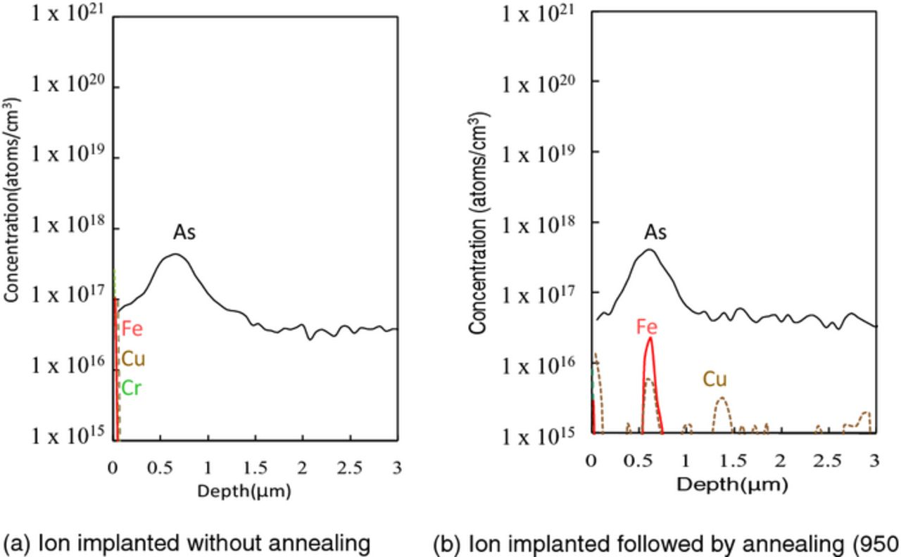
Figure 6. SIMS profiles of sub-surface metals in silicon implanted with arsenic through screen SiO2 (As dose: 1 × 10¹³ atoms/cm2).
It should be noted that surface metals penetrate silicon and are trapped in silicon dioxide during ion implantation, while subsequent annealing diffuse metals in the silicon dioxide, move into silicon. Thus, surface metal contamination can cause a carrier trap in silicon even when a screen oxide is present during ion implantation. Figure 7 shows the concentration of metals on the surface, metals in the 20 nm oxide, and sub-surface metals after ion implantation followed by annealing at 900°C for 20 min. Different metals penetrate to different depth of the sub-surface of silicon. The concentration of Cu on the silicon surface is extremely lower than other metals, while Cu concentration in the depth of ∼3 μm of silicon is not less than others. Most Cu is considered to be diffused deeper than the depth of ∼3 μm of silicon due to its high diffusion coefficient.1,21,22 This is the reason why the amount of surface Cu detected with TXRF after arsenic implantation and annealing was significantly lower than other metals as shown in Fig. 2a.
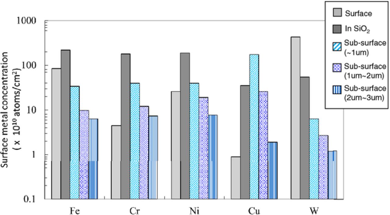
Figure 7. Sub-surface metal concentrations after arsenic ion implantation followed by annealing.
The concentration of W on the silicon surface is extremely higher than other metals, while W concentration in the depth of ∼3 μm of silicon is less than others. Most W is present on the silicon surface and in the oxide even after ion implantation and annealing. The atomic diameter of W is larger than the other metals. This will be the reason why W is most difficult to penetrate SiO2. Fe, Cr, and Ni are mostly trapped in silicon dioxide and some of them are diffused and traverse to the sub-surface of silicon. Metals such as Fe, Ni, and Cu can be trapped at the interface between SiO2 and Si.23,24 The metals trapped at the interface can be collected when SiO2 is dissolved by diluted HF solutions. The amount of metals estimated to present in SiO2 may include metals at interface, while the behavior of Fe and Cu in SiO2 and Si are different and Cu amount estimated to present in SiO2 is much smaller than Fe, as shown in Fig. 7. Therefore, an influence of metals trapped at the interface on the analysis is not significant. It is considered that Fe, Cr, and Ni have larger affinities for SiO2 than Cu and W. The rates of metals penetrating silicon sub-surface by the collision of metals with arsenic ion followed by annealing at 950°C for 10 min to surface metals (Fe, Cu, W) before ion implantation are shown as a function of SiO2 thickness in Fig. 8a. 0.1∼8% of surface metals penetrate silicon even when implanted through screen SiO2 film, depending on metal species and the SiO2 thickness. Here, Cu penetrates silicon through SiO2 more than Fe and W do at any thickness of SiO2. The rate of W penetrating silicon sub-surface through SiO2 decreases as an increase in SiO2 thickness while the penetrating rate of Fe and Cu do not always decrease with SiO2 thickness. As W will be a slow diffuser in SiO2 as well as in Si, W atoms take longer to reach the SiO2/Si interface. Thus, the amount of W penetrating silicon can be reduced. While Fe is a comparatively slow diffuser in SiO2, Fe atoms are supplied to Si from SiO2 storing large amount of Fe during subsequent annealing. Also Cu is a fast diffuser in SiO225 as well as in Si and passes through SiO2 to penetrate Si. Figure 8b shows the rate of metals (Fe, Cu, W) penetrating silicon sub-surface by arsenic ion implantation and different annealing temperatures and times. There is no significant difference in the penetrating rates of these metals in the range of 950–1000°C for 10–100 min. The penetrating rates of these three metals are in the range of 0.1∼8%.
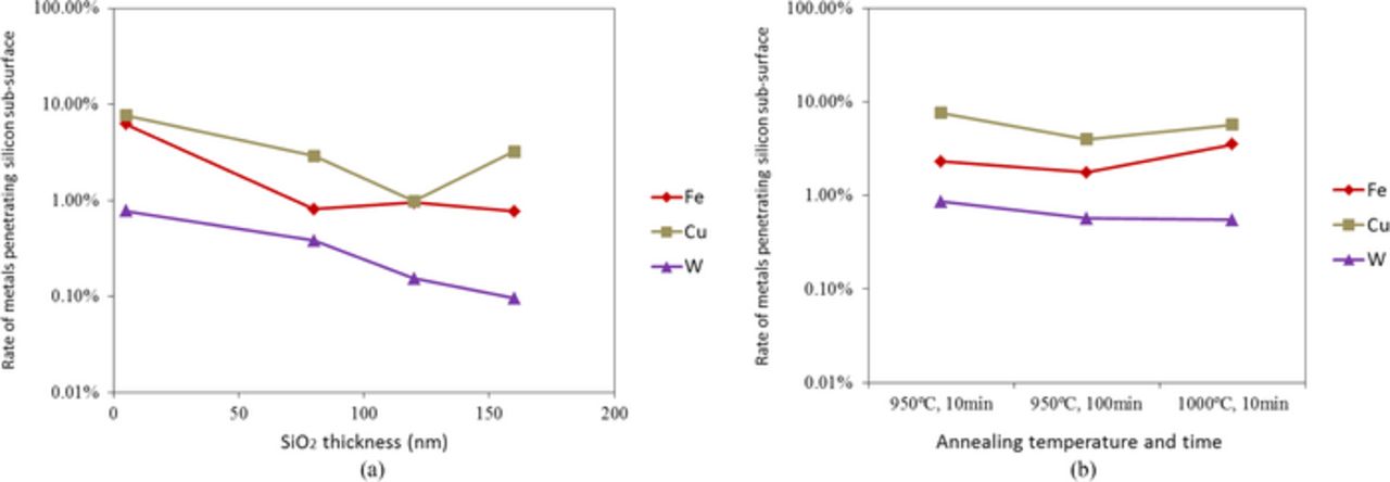
Figure 8. Rate of metals penetrating silicon sub-surface by arsenic ion implantation followed by annealing (a) with different SiO2 thickness at 950°C for 10 min and (b) with 80 nm SiO2 at different temperatures and times.
Carrier recombination in silicon due to low-level surface metals penetrating silicon
The distribution of the amounts of surface Fe and Ni concentration measured by a mapping TXRF before ion implantation and recombination lifetime after ion implantation followed by annealing are shown in Fig. 9. In this experiment, the concentration of surface Fe and Ni concentration was varied from 1.0 × 10¹⁰ to 1.3 × 10¹² atoms/cm2 in the wafers. The recombination lifetime after arsenic ion implantation of the wafers contaminated with Fe was varied from 23 μs to 43 μs, as shown Fig. 9b. As the amount of Fe contaminated before the implanataion is larger, the resultant recombination lifetime is shorter. The recombination lifetime of the wafers contaminated with even small amount of Fe as much as 1.0 × 10¹⁰ atoms/cm2 is significantly short. On the other hand, the recombination lifetime after arsenic ion implantation of the wafers contaminated with Ni is varied from 158 μs to 168 μs and is longer than that of Fe. Ni is more difficult to generate deep levels than Fe because interstitial Ni is not electronic active, but substitutional Ni is active and the amount of the substitutional Ni is not extremely small.26 This is the reason why the recombination lifetime of the wafer contaminated with Ni is longer than that of Fe. Nevertheless, the in-wafer distributions of surface Ni concentration before ion implantation shown in Fig. 9a is still in good agreement with that of recombination lifetime after ion implantation followed by annealing, same as Fe. The region of high concentration metals in the wafer before ion implantation yields carriers with a short lifetime after ion implantation even in 20-nm-thick SiO2 wafers. It should be noted that low level surface Fe and Ni contamination as little as 2 × 10¹¹ atoms/cm2 cangenerate carrier traps even when dopants were implanted through SiO2.
Quantification of metals penetrating silicon through screen silicon nitride films
The metal concentration on the surface, in the Si3N4 film, and in the sub-surface of the silicon after arsenic ion implantation and subequent annealing is shown Fig. 10. The initial concentration was 2 × 10¹³ atoms/cm2. Most of the Fe and Ni are present in the Si3N4 film rather than the silicon substrate, while most of the Cr, Cu, and W are no longer present in the Si3N4 film, but penetrate into the silicon substrate. In comparison with the metal concentration after only the annealing (without implantation) shown in Fig. 11, the Cr and W penetrate even more into the silicon substrate due to the dopant ion implantation. It is remarkable that W is penetrating more through Si3N4 films than through SiO2 films. The amount of Ni, Cu, and W in the Si sub-surface to 1 μm of the implanted wafers are larger than that of only the annealed wafers. It is assumed that these metals got trapped in the crystal defects (appropriately called end-of-range defects20) generated by the recrystallization after amorphousization. Fe, Cr and Ni penetrating silicon through the CVD Si3N4 films are compared with that through thermally-grown SiO2 films. Most Fe are on the surface and in the Si3N4 film same as SiO2 for screen film, as shown in Fig. 12. On the other hand, Cr and Cu diffuse through the Si3N4 film into the silicon substrate even more than through the SiO2, although the density of the CVD Si3N4 film is larger than that of the thermally grown SiO2.16
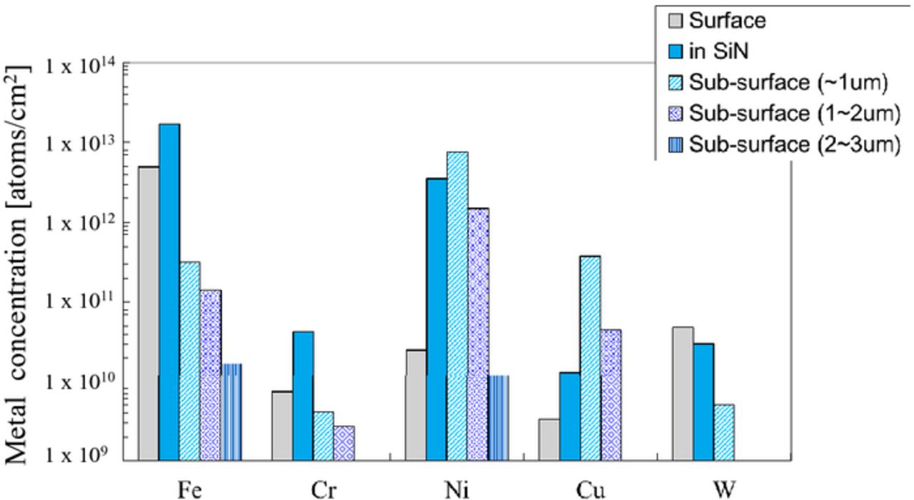
Figure 10. Depth distribution of metal concentration of the wafers implanted with arsenic through Si3N4 film followed by annealing.
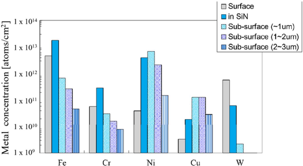
Figure 11. Depth distribution of metal concentration of the wafers Si3N4 film with after annealing.
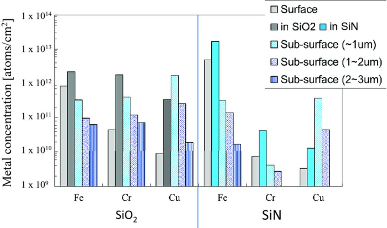
Figure 12. Depth distribution of metal concentration of the wafers implanted with arsenic through SiO2 or Si3N4 film followed by annealing.
The diffusion barriers of Fe, Cr and Ni in cristobalite SiO2 or β-Si3N4 were calculated by ab initio calculations.14,17,27 The diffusion barrier of Fe in β-Si3N4 is high and that of Cu in β-Si3N4 is low almost same as those in cristobalite SiO2, while the diffusion barrier of Cr in β-Si3N4 is smaller than that in cristobalite SiO2, as shown in Fig. 13. The diffusion barrier of Cr in the CVD Si3N4 film is also possibly smaller than that in the thermally-grown SiO2 film. Once the Cr penetrates the Si3N4 film, it diffuses into the Si3N4 film during annealing and reaches the interface of the SiN film and silicon substrate. Thus, Cr penetrates the silicon substrate under the Si3N4 film.
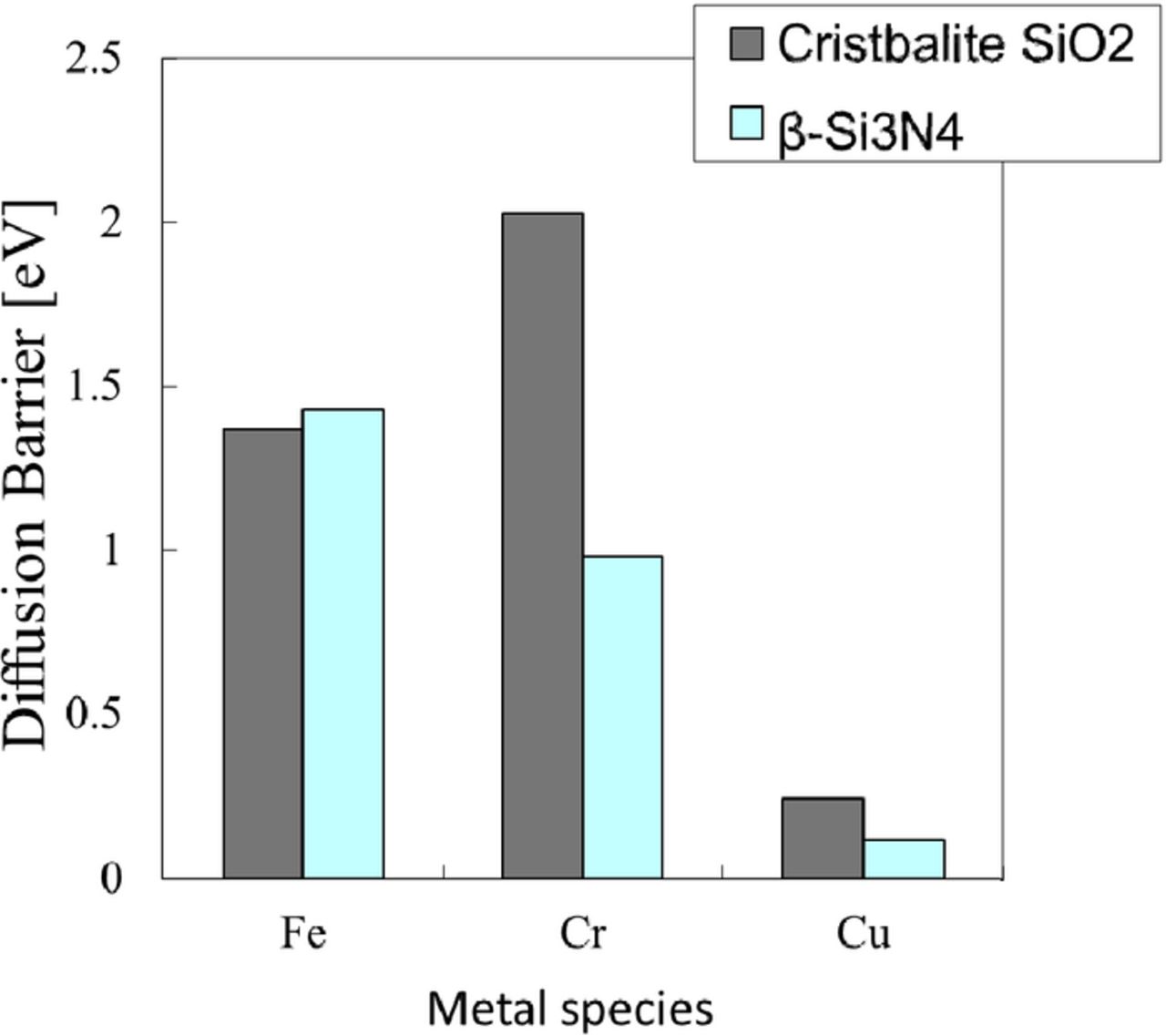
Figure 13. Calculated diffusion barrier of Fe and Cr in cristobalite SiO2 or β-Si3N4.
Conclusions
We have found that 0.1∼8% of surface metals penetrate silicon through screen silicon oxide or silicon nitride films by the collision of the surface metals and dopant atoms during arsenic ion implantation and subsequent annealing. When implanted, these metals are trapped in the screen films, while these metals diffuse in the screen film to penetrate silicon during the subsequent annealing. The depth of metals penetrating the silicon substrate during arsenic ion implantation and subsequent annealing is found to depend on metal species and the oxide thickness. W is most difficult to penetrate the SiO2 film, while W and Cr can easily penetrate Si3N4 films.
The recombination lifetime decreased by low level surface metals, as little as 2 × 10¹¹ atoms/cm2, penetrating even when implanted through SiO2. Thus, low level surface metal contamination can cause the generation of recombination centers even when a screen oxide is present during arsenic ion implantation.
The penetration of metals with a low diffusion coefficient in SiO2 such as W can be controlled by varying the SiO2 thickness. On the other hand, fast diffusers such as Fe and Cu penetrating silicon cannot be always reduced by an increase in the SiO2 thickness. Therefore, these metals must strictly be controlled in overall wafer processing.
The surface metals on a CVD Si3N4 film can penetrate into the silicon during ion implantation and/or subsequent annealing. We have found that Cr and W penetrate into silicon substrate more during dopant ion implantation. These metals penetrate the silicon substrate through the Si3N4 film more easily than through the thermally-grown SiO2. According to the ab-initio calculations of the diffusion barriers of metals in high temperature cristobalite SiO2 and β-Si3N4 whose atomic structures and densities are close to thermally grown SiO2 and CVD Si3N4, the diffusion barrier of Cr in the Si3N4 is lower than that in the SiO2. The CVD Si3N4 film and thermally grown SiO2 films can also have similar differences in the diffusion barriers, it can cause Cr easily penetrating silicon through Si3N4 film. Once the Cr penetrates the Si3N4 film, it diffuses into the Si3N4 film during annealing and reaches the interface between the Si3N4 film and silicon substrate. Thus, Cr penetrates the silicon substrate under the Si3N4 film. Therefore, these metals on Si3N4 films must be strictly controlled before ion implantation.
Acknowledgments
The authors acknowledge Dr. Takeno of Shin-Etsu Handotai Co. Ltd for the recombination lifetime measurement and fruitful discussion and to acknowledge Takahara of Technos Co. Ltd for the measurement of mapping TXRF.