
Abstract
In this work, we made network TiO2 nanowires of high surface area, using the seeded growth process. An overall solar photoconversion efficiency of 8.51% has been achieved from the film including TiO2 network nanowires, which is much higher than 6.94% of TiO2 nanoparticulate film with same thickness (6.2 μm).
Export citation and abstract BibTeX RIS
Excitonic solar cells
Including hybrid organic–inorganic, organic and dye-sensitized solar cells (DSSCs) are promising devices for inexpensive, large-scale solar energy conversion.1–6 The DSSC is currently the most stable and efficient excitonic photocell. The anodes of dye-sensitized solar cells are typically made using films of TiO2 nanoparticles that are deposited as a paste and sintered to produce electrical continuity.7–10 A key point to this device is the thick nanoparticulate film that provides a large surface area for the adsorption of light-harvesting molecules.11–13 To date, the highest solar conversion efficiency for dye-sensitized solar cells has been achieved with film that composed of nanocrystalline TiO2 nanoparticles.14–17 However, further increasing the solar conversion efficiency of DSSCs remains a challenge.
The transport of photogenerated electrons competes with recombination in DSSCs is a main bottleneck for developing higher solar conversion efficiency. A high-performance film requires that transport is significantly faster than recombination besides a large surface area for the adsorption of light-harvesting molecules.18 From the light intensity dependence of the electron diffusion coefficient in randomly packed TiO2 nanoparticulate films, it has been inferred that transport is limited by relying on trap-limited diffusion for electron transport, a slow mechanism that can limit device efficiencies.19 In TiO2 DSSCs, the use of a film constructed of one-dimensional crystalline nanowire arrays, has been found to enhance charge collection efficiency by promoting faster charge transport.19–22 However, these one-dimensional nanowire arrays reported previously are all independent entities with no ties to each other, which limits their solar conversion efficiencies to a relatively low level compared with that of a nanoparticles. Here we present the network nanowire film and illustrate how this topology could enhance the performance of DSSC.
Materials and Methods
Materials and methods
All chemicals (Tianjin Chemical Reagents Co.) used in our experiments were of analytical reagent grade without further purification. The film thickness was measured by using a Kosaka Lab. SE-2300 surface profilometer. The surface morphology of the films was observed on a Top con ABT-150FS scanning electron microscope (SEM). XRD measurements have been conducted using Bruker D8 Advance equipment following the Bragg Brentano measurement method. High-intensity green LEDs (530 nm), which led to a dc light at the electrodes, were used as intensity of up to 2.6 mWcm−2 light sources for IMPS and IMVS. The light intensities were modulated (±8%) by modulating the voltage applied to the LED with sinus waves in the frequency range from 0.2 Hz to 10 kHz for IMPS and from 0.02 to 200 Hz for IMVS. The dc and ac light intensities were measured with a calibrated photodiode. Neutral density filters were used to vary the light intensities down to about 0.1 mWcm−2. No corrections were made for absorption and reflection losses in the conductive glass. The transport time constants can be calculated from the expression τc = 1/2πfc, where fc is the characteristic frequency minimum of the IMPS imaginary component. Similarly, the recombination time constants can be determined from τr = 1/2πfr, where fr is the characteristic frequency minimum of the IMVS imaginary component.
Synthesis of network nanowires
The FTO substrate (Asahi Glass, 10 Ω/square, 0.8 × 0.8 cm2) was first cleaned thoroughly by propanetriol /acetone and then coated with a thin film of TiO2 nanowires, 10–15 nm in diameter, by dip-coating in ethanol solution. The substrate was placed within a sealed Teflon reactor (30 mL) containing 18 mL ethanol, 2 mL deionized water, 5 mM of Ti(OC2H5)4, 5 mM of triethanolamine, 3 mM of uridine and 3 mM of glucose at 160°C for 5 days. The substrate was repeatedly introduced to fresh solution baths in order to obtain dense network wires (total reaction times of up to 25 days). The substrate was then rinsed with deionized water and annealed in air at 450°C for 30 minutes to remove any residual organics from the TiO2 surface and to optimize cell performance.
Synthesis of electrolyte
0.5 mL of 1-Butyl-3-methylimidazolium tetrafluoroborate was mixed with 3.0 g of succinonitrile to give a clear liquid. Then a liquid electrolyte consisting of 0.5 M Bu4NI and 0.1 M I2 in the liquid 1-Butyl-3-methylimidazo liumtetrafluoroborate system was prepared. Finally, a stable gel electrolyte was obtained by mixing fumed silica nanoparticles (2 wt%) with the above liquid electrolyte through stirring and subsequently sonicating.
Fabrication of DSSCs
The network nanowire film and nanoparticulate film were immersed into a solution of 0.3 mM dye N719 or N749, 10 mL CH3CN and 10 mL t-butanol at room temperature for 12 h. The gel electrolyte was spin-coated onto the dye-absorbed TiO2 electrode, and kept in the vacuum oven for 2 h. The counter electrode was transparent conducting optical glass on which a 200 nm thick layer of Pt was deposited by sputtering. Subsequently, the cells were sealed with thermal adhesive films for the measurement.
Photoelectrochemical measurements
Photocurrent density-voltage curves of the DSSCs were measured under standard AM 1.5 solar illumination with an intensity of 100 ± 3 mWcm−2 using a computerized Keithley Model 2400 SourceMeter unit. A 1000 W xenon lamp (Thermo Oriel, USA) served as the light source. The active electrode area was typically 0.10 cm2. Monochromatic light in the range of 400 to 800 nm was obtained by using a series of filters, and the incident photo to current conversion efficiency (IPCE) measurement was performed on a Keithley Model 2400 SourceMeter.
Results and Discussion
One-dimensional nanostructures in previous papers are able to provide a direct pathway for the rapid collection of photogenerated electrons and reduce the degree of charge recombination, but the solar conversion efficiencies are limited mainly by the small internal surface area. We made network TiO2 nanowires of high surface area using the seeded growth process. The adsorption of krypton was used to measure the surface areas of the network nanowire film and the Brunauer-Emmett-Teller (BET) equation was used to calculate the network nanowire surface area from the adsorption branch. The result showed that network nanowire film had a high BET surface area of 48 m2/g, which is comparable to the BET surface area (anatase, from Aladdin (china), 53 m2/g) of the nanoparticles used in our experiment. Fig. 1 shows the scanning electron microscopy (SEM) images of the obtained TiO2 film. Fig. 1a indicates that the film was comprised of well stacked submicrometer-sized TiO2 network nanowires. The nanowires grow along the parallel direction. Thinner nanowires grow up on the thin nanowires. For a clearer view, Fig. 1b presents a magnified SEM image of the network TiO2 nanowires with diameters ranging from several to several tens of nanometers. The XRD pattern of network TiO2 nanowires is shown in Fig. 1c, indicating formation of the anatase phase.

Figure 1. Morphology of the network nanowires. (a) SEM image of the top view of the network nanowires. (b) A magnified SEM image of the network nanowires. (c) XRD pattern of the network nanowire film.
Because transport and recombination of photoinjected electrons are major determinants of the overall solar cell efficiency, thus, the study of these effects in network nanowire film is valuable for further advances in nanowire DSSC technology. Fig. 2 compares the transport and recombination time constants for the network nanowire and nanoparticulate films as a function of the light intensity I0. The thicknesses of the network nanowire and nanoparticulate films were 5.2 and 5.3 μm in the cells, respectively. For nanoparticulate film, the transport time constant τc (Figure 2a) displays nearly a power-law dependence on the light intensity. The cell containing the network TiO2 nanowire film displayed a τc of 8.1 × 10⁻⁴ s at the highest light intensity (8.85 × 1016 cm−2 s−1) and 7.3 × 10⁻³ s at the lowest light intensity (1.35 × 1015 cm−2 s−1). In contrast, the nanoparticulate film exhibited τc of 1.12 × 10⁻³ s at 8.85 × 1016 cm−2 s−1 and 1.16 × 10⁻² s at 1.35 × 1015 cm−2 s−1. The electron transport of the nanoparticulate photoelectrode was therefore slower than that of the network nanowire photoelectrode, presumably owing to it being limited the residence time of electrons in traps with both the particle network and the interparticle contact area. The network nanowires are good electrical conductors along the direction of the wire axes, indicating barrier-free contacts between the network nanowires and substrate. The better transport provided by an network nanowire film would be particularly favorable for cell designs that use gel electrolytes, such as polymer gels or solid-state dye-sensitized solar cells, in which recombination rates are high compared with the liquid electrolyte cell.
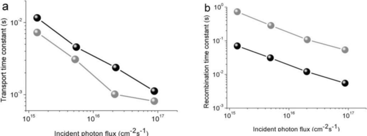
Figure 2. Comparison of transport and recombination time constants for network nanowire and nanoparticulate based DSSCs as a function of the incident photon flux for 610 nm laser illumination. Network nanowire TiO2 film = gray, nanoparticulate film = black.
The operation of solar cells is based on the competition of two basic processes. On the one hand, photoexcitation and charge separation forms a photocurrent, which is a flow of carriers toward the outercontacts. On the other hand, recombination is an opposite flow that internally annihilates the moving carriers. Figure 2b shows that the recombination time constant τr for the network nanowires was several orders of magnitude larger than that of the nanoparticulate film over the light-intensity range investigated. The cell containing the network nanowire TiO2 film exhibited a recombination time constant τr of 5.33 × 10⁻² s at the highest light intensity (8.85 × 1016 cm−2 s−1) and 0.72 s at the lowest light intensity (1.35 × 1015 cm−2 s−1). In contrast, the nanoparticulate film exhibited τr of 5.47 × 10⁻³ s at 8.85 × 1016 cm−2 s−1 and 0.069 s at 1.35 × 1015 cm−2 s−1. Intrinsic network nanowire surface states play an important role in this process, not only as electron traps but also as intermediate states for electron transfer to the electrolyte. The slower recombination could display that fewer potential surface recombination sites exist in network nanowires than in nanoparticulate film. Therefore, network nanowire film can be fabricated thicker than nanoparticulate film for a given recombination loss, which would allow for a higher light-harvesting efficiency, especially at the long-wavelength end of the visible light.
Figure 3 shows the short-circuit photocurrent density Jsc dependences of the network wire and nanoparticulate films on film thicknesses at 610 nm illumination. The incident photon flux I0 was held constant under AM 1.5 G illumination. The photocurrent densities are seen to increase with the thicknesses of both network nanowire and nanoparticulate films. However, the increase rate of Jsc with thickness for the network nanowire film was larger than that of the nanoparticulate film. The cell containing the network nanowire TiO2 film exhibited a Jsc of 15.37 mA.cm−2 at the thickest film (10.3 μm) and 3.33 mA.cm−2 at the thinnest film (1.1 μm). While for nanoparticulate film, the Jsc is 13.51 mA.cm−2 at the thickest film (10.2 μm) and 3.81 mA.cm−2 at the the thinnest film (1 μm). In as much as network nanowire and nanoparticulate films had comparable dye coverage and were exposed to the same redox electrolyte, the increase rates of Jsc vs film thickness was primarily determined by the charge-collection efficiencies ηcc. The ηcc for network nanowire and nanoparticulate films are determined from the expression: ηcc = 1−(τc/τr).18 The calculated ηcc at the highest light intensity (8.85 × 1016 cm−2 s−1) in Figure 2 for the network nanowire film was 23% larger than that of the nanoparticulate film, while that at the lowest light intensity (1.35 × 1015 cm−2 s−1) for the network nanowire film was 19% larger than that of the nanoparticulate film.

Figure 3. Comparison of the short-circuit photocurrent densities of dye-sensitized network nanowire and nanoparticulate cells as a function of film thickness. The cells were illuminated by a 610 nm laser under simulated AM1.5 light. Network nanowire TiO2 film = gray, nanoparticulate film = black.
Figure 4 displays the wavelength distribution of incident monochromatic photon to current conversion efficiency (IPCE). The IPCE spectra shows the external quantum efficiency of the cells peaks at 84.2% near the absorption maximum (554 nm) of the N719 molecules on the network nanowire TiO2 electrode. A very important aspect to this high IPCE value of the network nanowire film is that the network nanowires provide a large surface area for the adsorption of N719 molecules as large as that of a nanoparticulate film, leading to high light-harvesting efficiency. The maximum of IPCE in the visible region contributed by the N719 molecules absorption is located at approximately 548 nm with a value of 70.8% for the nanoparticulate film. It is clear that once the dissimilarity in the trasport and recombination processes arising from the different morphologies of the films are taken into account, the markedly enhancement in the IPCE value resulted predominantly from the increased charge collection efficiency ηcc value of the network nanowire TiO2 film.

Figure 4. IPCE of solar cells based on TiO2 films(6.2 μm thickness) sensitized with N719. Network nanowire TiO2 film = gray, nanoparticulate film = black.
Figure 5 and Table I compare the photocurrent density-voltage (J-V) properties of the network nanowire and nanoparticulate DSSCs. At comparable film thicknesses (6.2 μm thickness, Fig. 5), the network nanowire device is characterized by Jsc = 14.02 mA cm−2, open circuit voltage Vocp = 0.784 V, fill factor FF = 0.775 and solar conversion efficiency ξ = 8.51%. For comparison, the characteristics of the nanoparticulate film sensitized by N719 were also measured under similar conditions. The nanoparticulate solar cell exhibited FF = 0.758, Jsc = 12.69 mA/cm2, and Vocp = 0.751 V, yielding a solar conversion efficiency of 6.94%. The conversion efficiency of DSSCs containing a network nanowire film was about 22% higher than that containing a nanoparticulate film. This high solar conversion efficiency was accomplished by the specific morphology, in this case, the network nanowire film, which supplied a large surface area, comparable to that of a nanoparticulate film for the adsorption of N719 molecules to yield a high IPCE value. Because the network nanowire and nanoparticulate photoelectrodes had comparable N719 dye coverage and were exposed to the same redox electrolyte, it is reasonable to presume the similar initial number of photogenerated carriers for the network nanowire and nanoparticle photoelectrode. Thus, the enhancement of the conversion efficiency must predominantly result from important differences in the charge collection efficiency of the network nanowire film. Table I shows that with the increase of the thickness, the performance increases. However, the performance with thickness larger than 8 μm increases slightly. It is clear, the solar conversion efficiencies of the N749-based DSSCs are markedly higher than those of N719-based DSSCs for comparable film thicknesses.
Table I. J-V Characteristics of Dye-Sensitized Nanoparticulate and Network Nanowire Solar Cells under Simulated AM 1.5 Light.
| film and dye type | L (μm) | Jsc (mA/cm2) | Vocp (V) | FF | ξ (%) |
|---|---|---|---|---|---|
| nanoparticulate film sensitized with N719 | 7.5 | 12.94 | 0.754 | 0.757 | 7.38 |
| 8.5 | 13.36 | 0.756 | 0.752 | 7.59 | |
| 10.1 | 13.51 | 0.762 | 0.751 | 7.72 | |
| 11.8 | 13.57 | 0.753 | 0.754 | 7.70 | |
| network nanowire film sensitized with N719 | 7.2 | 14.76 | 0.782 | 0.773 | 8.92 |
| 8.2 | 15.28 | 0.787 | 0.775 | 9.31 | |
| 10.3 | 15.37 | 0.783 | 0.772 | 9.29 | |
| 12.3 | 15.52 | 0.785 | 0.779 | 9.49 | |
| network nanowire film sensitized with N749 | 6.3 | 14.71 | 0.794 | 0.768 | 8.97 |
| 7.4 | 15.68 | 0.794 | 0.774 | 9.63 | |
| 8.6 | 15.94 | 0.791 | 0.773 | 9.75 | |
| 10.2 | 16.12 | 0.789 | 0.773 | 9.83 | |
| 12.1 | 16.22 | 0.792 | 0.775 | 9.95 |

Figure 5. Photocurrent-voltage characteristics of solar cells based on TiO2 films(6.2 μm thickness) sensitized with N719. Network nanowire TiO2 film = gray, nanoparticulate film = black.
Conclusion
The network nanowire dye-sensitized solar cell is an exciting variety of the most successful of the excitonic photovoltaic devices. For a given film thickness, the network nanowire had shorter electron transport time and several times slower recombination than those of a nanoparticle photoelectrode, indicating that the charge-collection efficiency of the network nanowire photoelectrodes was extraordinarily enhanced. We are now extending our synthetic strategy to design denser nanowires with much larger area available for dye adsorption.
Acknowledgment
This work was supported by the Science and Technology Research Projects of the Education Office of AnHui Province (No. KJ2012Z348).