

Abstract
The traditional von Neumann structure computers cannot meet the demands of high-speed big data processing; therefore, neuromorphic computing has received a lot of interest in recent years. Brain-inspired neuromorphic computing has the advantages of low power consumption, high speed and high accuracy. In human brains, the data transmission and processing are realized through synapses. Artificial synaptic devices can be adopted to mimic the biological synaptic functionalities. Nanowire (NW) is an important building block for nanoelectronics and optoelectronics, and many efforts have been made to promote the application of NW-based synaptic devices for neuromorphic computing. Here, we will introduce the current progress of NW-based synaptic memristors and synaptic transistors. The applications of NW-based synaptic devices for neuromorphic computing will be discussed. The challenges faced by NW-based synaptic devices will be proposed. We hope this perspective will be beneficial for the application of NW-based synaptic devices in neuromorphic systems.
Export citation and abstract BibTeX RIS

Original content from this work may be used under the terms of the Creative Commons Attribution 4.0 license. Any further distribution of this work must maintain attribution to the author(s) and the title of the work, journal citation and DOI.
Future perspectives
NW artificial synaptic devices show great potential applications for brain-inspired neuromorphic computing. The device performance is dependent on the properties of NW materials and the structures of devices. It is of great significance to improve the device performance by growing novel NW materials, designing novel device structures and making special treatment on the materials and devices.
1. Introduction
With the rapid development of big data analysis, artificial intelligence and internet of things, the traditional von Neumann structure computers cannot meet the demands of high-speed big data processing [1–4]. In this case, neuromorphic computing has been rapidly developed [5]. Neuromorphic computing is inspired by human brains. There are an enormous number of neurons and synapses in human brains [6, 7]. The spike signals are transmitted from one neuron to another through synapses. Depending on the neural network (NN), the human brain can realize processing information with high speed, low power consumption and high accuracy [8–10]. Mimicking the synaptic functionalities of the human brain is essential for neuromorphic computing. To date, artificial synaptic devices have received widespread attention. Various synaptic devices, including synaptic memristors [11] and synaptic transistors [12], have been successfully fabricated to imitate biological synaptic functionalities.
The signal transmission efficiency in biological synapse is associated with the synaptic weight, which is defined as the connection strength between pre-synaptic and post-synaptic neurons. The change of synaptic weight is called synaptic plasticity, including short-term plasticity, long-term plasticity, spike-rating-dependent plasticity (SRDP) and spike-timing-dependent plasticity (STDP), etc [13–15]. For short-term plasticity, it contains short-term potentiation/depression (STP/STD), paired pulse facilitation/depression (PPF/PPD) and spike-number-dependent plasticity (SNDP) [16]. Long-term plasticity includes long-term potentiation/depression (LTP/LTD). SRDP describes the relationship between synaptic plasticity and spike frequency [17]. STDP explains the dependence of synaptic plasticity on time sequence and interval between presynaptic spikes and postsynaptic spikes [16]. By adjusting the spike parameters, short-term plasticity can convert into long-term plasticity [18–21]. To promote the practical application of neuromorphic computing, it is important to explore new materials and design novel synaptic devices.
To improve the integration of devices, nanostructured synaptic devices have been widely investigated, including quantum dots [22], nanowires (NWs) [23, 24] and two-dimensional (2D) materials [25, 26]. Due to the quasi-one-dimensional (1D) structure, NWs have the advantages of high aspect ratio, high carrier mobility and large surface-to-volume ratio, which have made them become important building blocks for nanoelectronics and optoelectronics [27–29]. Compared with 2D materials, NWs are more suitable for high integration and low power consumption synaptic devices. Nowadays, NWs have been integrated into diodes [30], field effect transistors (FETs) [31], memories [32], photodetectors [33], solar cells [34], and synaptic devices [19, 23, 35]. Based on the basic synaptic functionalities of NW-based synaptic devices, NWs can be constructed for neuromorphic computing.
Here, we will introduce the current research process for NW-based synaptic devices, including NW-based synaptic memristor and NW-based synaptic transistor. Then the applications of NW-based synaptic devices for neuromorphic computing are discussed. Finally, the challenges faced by NW-based synaptic devices are proposed. The overview of this perspective is summarized in figure 1.

Figure 1. Overview of this perspective.
Download figure:
Standard image High-resolution image2. Nanowire-based synaptic memristor
Depending on the device structure, NW-based synaptic devices are mainly divided into two categories, i.e. NW-based synaptic memristor and NW-based synaptic transistor. Memristors can be fabricated into vertical or lateral structures [36–38]. Memristors integrate computing and memory units in the same location, which have the advantages of high integration and low power consumption [39]. The current–voltage (I–V) hysteresis of memristor is used for the information storage and processing. By adjusting the operation parameters, resistive switching properties between high resistance state and low resistance state (LRS) are realized. Volatile and nonvolatile memristors have been widely studied, where the volatile memristors usually have a short retention time on LRS and the nonvolatile memristors usually have a longer one [40]. Ni/NiO core–shell NWs were fabricated into crossbar memristor [36]. Owing to the diffusion of oxygen ions under electric field, conductive filament was formed or broken at the crossbar center, thus nonvolatile resistive switching behavior was observed. A device network based on Ag NWs coated with TiO2 was prepared by Li et al [41]. To fabricate the device network, NW solution was dropped onto the substrate with pre-patterned electrodes. The device structure diagram is shown in figure 2(a). The electrical properties of the device network were characterized and the I–V curves are shown in figure 2(b). An obvious current hysteresis was observed as the voltage swept from 0 to 130 V and back again. Besides, the conductivity increased during continuous voltage sweeping. This behavior was similar as the synaptic functionality of STP. When voltage was swept from −130 to 130 V over and over again, resistive switching behaviors could be observed in the NW device network, where the LRSs were realized by the low resistance pathway between at least two NWs. The memristive behavior of Ag2S NW networks memristor had also been investigated by Hosseini et al [42]. The synaptic functionalities, including learning and forgetting processes have been mimicked by the memristor. The results promote the application of NW networks for reservoir and neuromorphic computing.

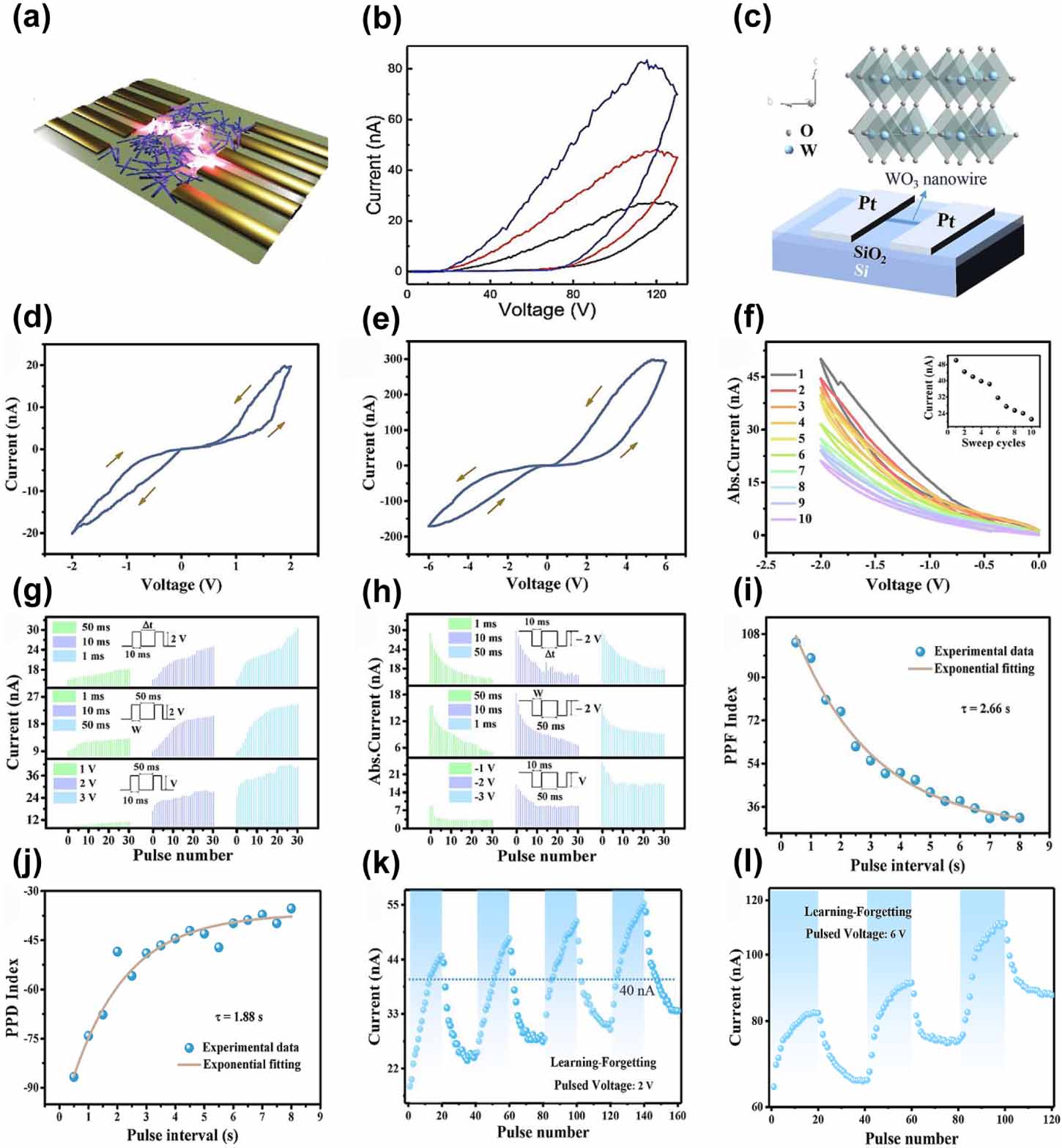
Figure 2. (a) The device structure diagram of Ag NWs coated with TiO2 network. (b) I–V curves. (c) The schematic diagram of the WO3 NW memristor, the inset is the material structure. (d) Resistive switching properties when the operation voltage is 2 V. (e) Resistive switching properties when the operation voltage is 6 V. (f) Continuous sweeping negative I–V curves of the memristor at −2 V. (g) Dependence of EPSC and intervals, pulse durations, voltage strengths. (h) Dependence of IPSC and intervals, pulse durations, voltage strengths. (i) PPF. (j) PPD. (k) Learning-forgetting experience when the electrical pulse is 2 V. (l) Learning-forgetting experience when the electrical pulse is 6 V. (a)–(b) [41] John Wiley & Sons. [© 2020 Wiley-VCH GmbH]. (c)–(l) Reprinted from [43], with the permission of AIP Publishing.
Download figure:
Standard image High-resolution imageIn addition to the conductive filament working mechanism of memristor, Schottky barrier can also result in resistive switching behavior. ZnO NW memristor with back-to-back Schottky structure was designed [37]. The resistive switching behavior was realized by the Schottky barrier tunneling current. A WO3 NW based two-terminal memristor was prepared by Qin et al [43]. The schematic diagram of the device and the material structure are shown in figure 2(c). By adjusting the voltage, the device exhibited bipolar nonvolatile and volatile resistive switching properties. As shown in figure 2(d), when the operation voltage was 2 V, the memristor showed nonvolatile resistive switching properties. When the operation voltage was 6 V, as shown in figure 2(e), the nonvolatile resistive switching properties would transfer to volatile resistive switching properties. Furthermore, the current strengthening behaviors were observed at both of two operation voltages when sweeping at positive voltages. However, when sweeping at negative voltages, the weakening behavior was realized at −2 V, and the strengthening behavior was realized at −6 V. Figure 2(f) shows the continuous sweeping negative I–V curves of the memristor at −2 V, illustrating the current weakened trend of the memristor. This could be explained by the oxygen vacancies based resistive switching mechanism and the metal-semiconductor contact barrier. There are many oxygen vacancies in WO3 NWs. Under positive voltage, when the operation voltage was small, the resistive switching properties were dominated by conductive filament, and a reverse voltage was required to break the conductive filaments. When the operation voltage was large, the resistive switching properties were dominated by contact barriers. The contact barrier would be reduced in both positive and negative voltages, and the resistive switching properties were volatile. The resistive switching properties could be used to mimic synaptic functionalities. As shown in figures 2(g)–(l), the excitatory postsynaptic current (EPSC), inhibitory postsynaptic current (IPSC), PPF and PPD had been mimicked by the memristor. The EPSC and IPSC were dependent on the pulse interval time, pulse durations and voltage strengths. Besides, the learning-forgetting experience had been simulated, and it suggests that the WO3 NW-based memristors have the potential to construct intelligent neuromorphic devices.
To adjust the memristive behavior of NW memristor, Shan et al studied the synaptic plasticity of TiO2 NW memristor before and after plasma treatments [44]. The device structures are shown in figure 3(a), and Ar-H2 plasma treatment was applied to the device. As shown in figures 3(b) and (c), for the pristine TiO2 NWs, the current would increase gradually when sweeping at positive voltages. After several sweeps, the current reached saturation. When sweeping at negative voltages, the change in current was negligible. This kind of memristive behavior could be considered as a silent synapse. After treated by Ar-H2 plasma, the current would change at both positive and negative voltages, meaning that the memristor was a functional synapse. Besides, the change in current after plasmas treatment was more obvious than the untreated device. This could be explained by the increased oxygen defects after plasma treatment. Plasma treatments under different gas atmospheres were proposed to adjust the synaptic activity. As shown in figures 3(d)–(f), different gas plasma treatments led to different synaptic plasticity, which were related to the different oxygen vacancies caused by plasma treatments. Wan et al had also studied the synaptic learning rules of single ZnO NW memristor after Ar plasma treatment [45]. Figure 3(g) shows the schematic diagram of a synapse and the SEM image of the device. According to the I–V curves of the device in figure 3(h), after plasma treatment, the device showed a lower operation voltage (5 V) than that in untreated device (10 V). It means the device power consumption could be reduced by plasma treatment. Then, the STDP, SRDP and synaptic-voltage-dependent plasticity (SVDP) properties of the device had been mimicked, and the results are given in figures 3(i)–(k). As seen in the STDP and SVDP result, plasma treatment would increase the change of synaptic weight, thus the learning capability would be strengthened. For SRDP, the change of synaptic weight before and after plasma treatment was negligible. The dependence of conductance and pulse number is shown in figure 3(l). For both of untreated and plasma treated devices, the conductance was first increased with the growth of pulse number quickly and then reached saturation. For the plasma treated device, it needed more pulse numbers to reach saturation, which also means the learning capability had been facilitated by plasma treatment.

Figure 3. (a) Device structures of TiO2 NW-based memristor before and after plasma treatments. (b) The I–V curves of pristine TiO2 NWs. (c) The I–V curves of TiO2 NWs after Ar-H2 plasma treatment. (d) EPSC of the device after different gas plasma treatments. (e) SNDP. (f) STDP. (g) Schematic diagram of a synapse and the SEM image of the single ZnO NW memristor. (h) I–V curves of the device. (i) STDP. (j) SRDP. (k) SVDP. (l) Dependence of conductance and pulse number. (a)–(f) [44] John Wiley & Sons. [© 2020 Wiley-VCH GmbH]. (g)–(l) Reproduced from [45]. © IOP Publishing Ltd. All rights reserved.
Download figure:
Standard image High-resolution imageTo promote the application of NW-based memristor for neuromorphic computing, memristors with enhanced synaptic weight, high stability and lower power consumption need to be further explored. Besides plasma treatment, cation injection and laser radiation are also good choice to modulate the defects of materials. Besides, design of device structure and material structure can also improve device performance. For example, the stability of memristor can be significantly improved by alloying conducting channels [46], and excellent resistive switching behavior and synaptic plasticity could be realized by ZnO nanoparticles/CuO NW heterostructure memristor [47]. Thus, more feasible schemes should be further explored.
3. Nanowire-based synaptic transistor
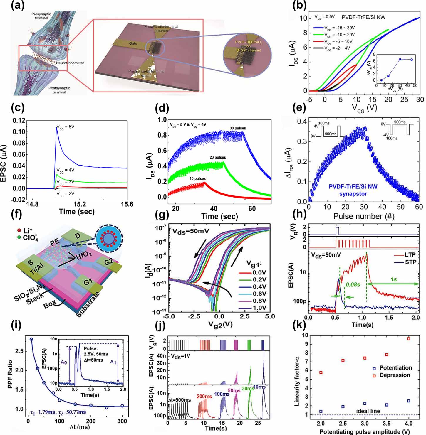
Although NW-based memristors have the advantages of low power consumption and high integration, sneak currents are usually caused by operating memristors on a large scale. Besides, memristor also faces the challenges in mimicking the biological synapses because the signal transmission and learning processes of memristors will happen at the same path. For FETs, there are three terminals in the device and they can realize signal transmission and learning simultaneously. Besides, the channel conductivity can be adjusted by the gate [48]. Si NW ferroelectric complementary metal-oxide-semiconductor (CMOS) FET had been demonstrated for application as nonvolatile memory [49]. The device displayed ultralow power consumption. Lee et al had also demonstrated a Si NW ferroelectric FET (FeFET) [50]. The schematic illustration of the Si NW synaptic FeFET is shown in figure 4(a). The electrodes were first patterned by e-beam lithography, then the plasma chemical vapor deposition was used to deposit SiO2 on the device. Finally, spin-coating method was used to prepare PVDF-TrFE layer. For the transfer characteristic of the Si NW FET, the device showed unobvious hysteresis window, and the hysteresis window was larger in the Si NW FeFET. The transfer characteristics of Si NW FeFET with different sweep ranges are shown in figure 4(b). It could be seen that when the sweep range became larger, the hysteresis window became larger as well, which indicated the device had the potential to be applied to artificial synaptic devices. The dependence of EPSC and pulse voltage had been studied and the result is shown in figure 4(c). A transition from STP to LTP was observed when the pulse voltage became larger. Besides, the SNDP of the device is shown in figure 4(d). With the increase in pulse number, the decay time of the current became longer. The potentiation and depression behaviors of Si NW FeFET under a few voltage pulses were demonstrated in figure 4(e). They showed high linearity and excellent symmetry, which could be further optimized by changing the pulse voltage. The excellent synaptic plasticity of Si NW FeFET makes it suitable for neuromorphic computing systems.

Figure 4. (a) The scheme of the Si NW-based synaptic FeFET. (b) The transfer characteristics of the Si NW FeFET with different sweep ranges. (c) The dependence of EPSC and pulse voltages. (d) SNDP. (e) LTP/LTD. (f) Schematic diagram of the ionic-gated Si NW synaptic FET. (g) Transfer characteristics of the device under the modulation of two gates. (h) STP and LTP. (i) PPF. (j) SRDP. (k) Dependence of linearity factor and pulse voltage. (a)–(e) Reprinted from [50], with the permission of AIP Publishing. (f)–(k) Reproduced from [51] with permission from the Royal Society of Chemistry.
Download figure:
Standard image High-resolution imageAn ionic-gated Si NW synaptic FET was fabricated by CMOS compatible technology [51]. Figure 4(f) shows the schematic diagram of the device, where ten parallel NWs and two modulation gates had been integrated into one device. There were obvious hysteresis windows in the transfer characteristics of the device under the modulation of two gates, where gate2 was set to the first variable, and gate1 was set to the second variable, which are shown in figure 4(g). These hysteresis windows could be explained by the ion migration and lagged dispersion between the NWs and gate electrodes. Besides, there was gate coupling effect between the two gates. With the increase of gate1 voltage, the threshold voltage would shift negatively, which may be related to the accumulation of extra ions. The synaptic plasticity of the device was further investigated. The STP, LTP, PPF and SRDP could be well mimicked by the device, and the results are shown in figures 4(h)–(k). The power consumption of per synaptic event was as low as 375 fJ, showing great potential for low-power artificial synapses. The good PPF and SRDP properties make the device suitable for information decoding and transmission. Furthermore, the LTP/LTD was also studied and the linearity factor was extracted. The linearity factor could be optimized by adjusting the pulse voltage, showing that the two gates have excellent control ability on ionic accumulation.
Many efforts have been made by researchers in NW-based synaptic transistors. However, the multi-functionality of devices is limited by the pure electrical input and output [52]. Besides, the operation speed and the power consumption are not ideal in pure electrical synaptic devices [53, 54]. To overcome these disadvantages, optoelectronic synaptic devices have been introduced and developed [55, 56]. Various synaptic functionalities had been mimicked by NW-based optoelectronic synaptic devices [19, 23, 35, 57, 58]. A SnO2 NW optoelectronic synaptic transistor had been demonstrated, where the gate dielectric was composed of electrolyte gel [59]. The device structure is shown in figure 5(a). The optoelectronic characteristic of the device was studied. From the transfer characteristic curves as shown in figure 5(b), the current would become larger and the threshold voltage would shift negatively under UV illumination. To study the synaptic plasticity of the device, the PPF was successfully mimicked and the PPF index was extracted, as shown in figures 5(c) and (d). The PPF index was dependent on the gate bias, which determines the carrier trapped on the device surface and interface. This was called the photogating effect. Photogating effect is usually caused by the rich surface states of the NWs. Lots of photo-generated charges are trapped at the surface and interface between the NWs and the dielectric. The trapped charges will produce an extra electric field and modulate the conductance of the NWs. The life time of photo-generated carriers in the device working on photogating effect is relatively long, and the PPF will be produced. When a gate bias is applied on the device, the carrier concentration of the NWs is changed, resulting in the change in the modulate ability of the trapped charges. Thus the PPF index is dependent on the gate bias. Besides, the power consumption of per synaptic event was hundreds of picojoules in this device, which was still higher than that in human brains [6, 8, 9]. Li et al proposed an InAs NW synaptic phototransistor [60]. The device structure is shown in figure 5(e). Due to the intrinsic oxide layer on the surface of the NW, photogating effect also played a major role in mimicking synaptic behaviors. It was worth noting that the device had negative photoconductive response. Under illumination, the photo-generated electrons are trapped by the intrinsic oxide layer, and the photo-generated holes are recombined with the intrinsic electrons, resulting in the decrease of photocurrent. By adjusting the light intensity, the STD could change to LTD, as shown in figures 5(f)–(g). The PPD behavior could be also mimicked and the PPD index is shown in figure 5(h). The dependence of PPD index and pulse interval time demonstrated the InAs NW synaptic phototransistor was suitable for mimicking human brains. Zha et al further studied the negative photoresponse of InAs NW phototransistor [61]. The synaptic plasticity could be adjusted by gate voltage and light intensity. STD and LTD could be successfully mimicked. Besides, the negative photoresponse was related to the gate voltage, light intensity, and traps concentration. By adjusting these parameters, the negative photoresponse would change to positive photoresponse, which is beneficial for all-optical operation optoelectronic synaptic devices. However, a stronger light intensity needs to be used to operate the devices, which may be related to the photo-sensitivity of the materials. Several strategies can be implemented to decrease the operating light intensity, such as introducing two-dimensional electron gas [23, 62] and manufacturing heterojunction [19], which can effectively improve the photo-sensitivity of the materials. This negative and positive photoresponse behavior had also discovered in other materials. Si NW phototransistors were proposed to mimic artificial synapse [20]. Negative photoresponse was observed in n-type Si NW phototransistor, and positive photoresponse was observed in p-type Si NW phototransistor. This phenomenon could be explained by the electron transfer process between porphyrin molecules and Si NWs. Figures 6(j)–(l) show the PPD and PPF behavior. Besides, the IPSC are also dependent on the gate voltage, which was helpful for establishing visual NN. Besides photogating effects, Schottky barrier [63] and p-n junction [64] are also good strategies for the realization of optoelectronic synaptic devices, which could be developed in future research.

Figure 5. (a) Device structure of a SnO2 NW optoelectronic synaptic transistor. (b) Transfer characteristic curves with different solar blind ultraviolet light intensities. (c) PPF. (d) PPF index. (e) Device structure of InAs NW phototransistor. (f) STD. (g) LTD. (h) PPD index. (i) Device structure of Si NW phototransistor. (j) PPD. (k) PPF. (l) Dependence of IPSC and gate voltage. (a)–(d) Reprinted from [59], Copyright (2019), with permission from Elsevier. (e)–(h) Reproduced from [60]. © IOP Publishing Ltd. All rights reserved. (i)–(l) [20] John Wiley & Sons. [© 2021 Wiley-VCH GmbH].
Download figure:
Standard image High-resolution image
Figure 6. (a) WO3 NW synaptic memristor for pattern recognition. (b) Back-propagation algorithm process. (c) Simulation of the MNIST pattern recognition based on Si NW synaptic FeFET. (d) LTP/LTD in ZnO NW optoelectronic synaptic transistor. (e) Change of current weight in potentiation and depression processes in ZnO NW optoelectronic synaptic transistor. (f) Recognition accuracy. (a) Reprinted from [43], with the permission of AIP Publishing. (b)–(c) Reprinted from [50], with the permission of AIP Publishing. (d)–(f) Reproduced from [58]. © IOP Publishing Ltd. All rights reserved.
Download figure:
Standard image High-resolution imageNW-based synaptic transistors have been widely studied, including electronic FETs and optoelectronic FETs. The synaptic functionalities are realized by operating the NW-based synaptic devices. Researchers have proposed that neuromorphic synaptic devices need to meet the following performance indicators: high linearity of conductance, the ratio of maximum conductivity and minimum conductivity should be larger than 10, the data levels should be larger than 32, and small variation of cycle-to-cycle/device-to-device performance [65, 66]. To further improve the NW device performance and promote the application of the NW-based synaptic devices for neuromorphic computing, future researches should focus on exploring new NW materials and designing new NWstructures. For example, floating gate transistors show outstanding advantages in data retention [67], superlattice structures are beneficial for carrier regulation and power consumption [23, 68, 69].
4. Neuromorphic computing based on nanowire synaptic devices
Neuromorphic computing is realized by artificial synaptic devices through mimicking the structure and function of the human brain. NNs are usually constructed based on artificial synaptic devices, and then further applied in neuromorphic computing. Pattern recognition is a typical neuromorphic computing [70, 71], which requires that the NNs constructed by synaptic devices can identify the typical features of digital images, and the recognition accuracy is high [72, 73]. Both NW-based synaptic memristors and NW synaptic transistors have been used for pattern recognition. A WO3 NW synaptic memristor was proposed for pattern recognition [43]. As shown in figures 6(a), a three-layer ANN was constructed to recognize handwritten digits. The handwritten digits were divided into a plurality of pixels, and the pixels were entered into the input layer. The input signals were processing in hidden layer, then the recognition results were given by output layer. According to the LTP/LTD properties, the simulated recognition accuracy was 94% when recognizing an 8 × 8 pixels image and would reduce to 85% when recognizing a 28 × 28 pixels image after training for 40 epochs. Wang et al proposed digital-analog integrated memristor based on CuO NW heterostructure [47], and the device was used for simulating to recognize handwritten digits. The recognition accuracy reached to 93% under supervised learning. A back-propagation algorithm based three-layered ANN was constructed from Si NW synaptic FeFET [50], as shown in figure 6(b). After training for 40 epochs, the recognition accuracy reached to 85.1% when recognizing a 28 × 28 pixels MNIST image.
Optoelectronic synapses have the potential to simulate artificial vision, and are suitable for constructing ANNs for pattern recognition. Shen et al proposed a ZnO NW optoelectronic synaptic transistor to recognize handwritten digits, where the potentiation process was realized by light stimulating, and the depression process was realized by electrical stimulating [58]. The potentiation and depression processes are shown in figures 6(d) and (e). Based on the excellent LTP/LTD properties of the device, the recognition accuracy reached up to 92% after only 20 training epochs when recognizing a 16 × 16 pixels image.
In addition to ANN, spiking neural networks (SNN) were also a good choice for pattern recognition. The difference between ANN and SNN is the type of input signals [74]. For ANNs, the input signals are continuous signals, and the input signals in SNNs are usually encoded into binary spike trains. An ionic-gated Si NW synaptic FET SNN was performed for pattern recognition based on unsupervised learning [51]. Compared with supervised learning, unsupervised learning has the advantages of low cost, low power consumption, and has the ability to learn the unlabeled data. But the recognition accuracy of unsupervised learning was usually lower than that in supervised learning. Figures 7(a) and (b) illustrate the recognition results when using the SNN for pattern recognition. A recognition accuracy of 84.6% was obtained after 60 000 training instances. To further improve the accuracy, the linearity of the synaptic should be optimized.

Figure 7. (a) Dependence between recognition rate and training iterations in ionic-gated Si NW synaptic FET SNN. (b) Dependence between recognition rate and output neurons. (c) Core–shell dual-gate NW synaptic transistor for HNN. (d) Recognition accuracy of the HNN when the image was 28 × 28 pixels. (e) Schematic diagram of the single layer perceptron HNN. (f) Training results. (g) Schematic diagram of Ag NW networks memristive device for reservoir computing. (a)–(b) Reproduced from [51] with permission from the Royal Society of Chemistry. (c)–(d) Reproduced from [75]. CC BY 4.0. (e–f) Reprinted from [24], Copyright (2022), with permission from Elsevier. (g) Reproduced from [77], with permission from Springer Nature.
Download figure:
Standard image High-resolution image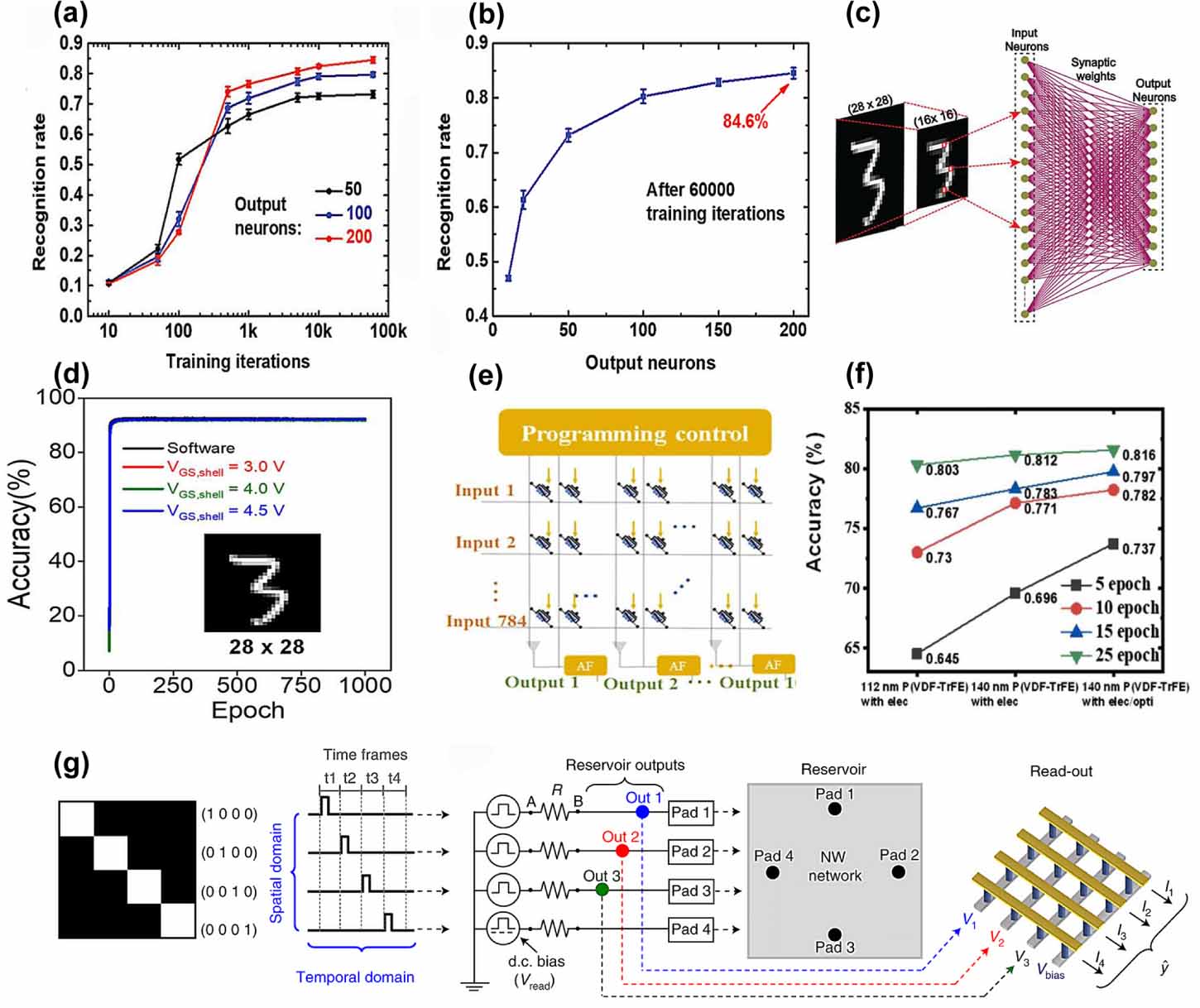
Actually, either ANNs or SNNs can be called as hardware neural networks (HNNs) as long as they are integrated into hardware. A simulated core–shell dual-gate NW synaptic transistor had been constructed into a single-layer HNN [75]. To simulate the supervised learning capability of the device, the HNN was used to classify the image data from MNIST database. It was found that the recognition accuracy was dependent on the gate voltage and image pixels. The results are shown in figures 7(c) and (d). When the gate voltage was 4.5 V, after training for 1000 epochs, the recognition accuracy reached up to 92.28% when the image was 28 × 28 pixels, and reduced to 90.17% when the image was 16 × 16 pixels. A simulated HNN was constructed by P(VDF-TrFE) wrapped InGaAs NW synaptic transistors for pattern recognition [24]. The recognition accuracy could reach up to 80% only after a few trainings, exhibiting lower power consumption.
NWs synaptic devices can also be used for reservoir computing, which enable to processing temporal and spatial signals [76]. Self-organized Ag NW networks memristive device have been proposed for reservoir computing [77]. The schematic diagram of the device for reservoir computing is shown in figure 7(g). The device showed nonlinear synaptic plasticity and short-term memory behavior, and spatio-temporal patterns could be recognized.
In addition to pattern recognition, neuromorphic computing can also be used for image processing, speech recognition and motion monitoring [78]. However, NW synaptic devices have been rarely studied for applications in these areas. Perovskite NW memories have been used for image processing [79]. Due to the multi-level switching behavior of the device, the image was successfully embossed, outlined and sharpened. Ag NW nanocomposite hydrogel sensor has been fabricated and the device could be used for human motion detection [80]. Future research should further expand the applications of NW synaptic devices in neuromorphic computing.
5. Challenges and outlook
In summary, we have summarized the recent development of NW-based synaptic devices and their applications for neuromorphic computing. NW-based synaptic devices have successfully mimicked synaptic functionalities, including STP/STD, LTP/LTD, STDP, and so on. By applying NW-based synaptic devices into NNs and reservoir, pattern recognition and spatio-temporal signal recognition are realized. However, there are still some challenges faced by NW synaptic devices, including the stabilities of NWs and devices, the power consumption, the neuromorphic interconnection, and the on-chip integration. Additionally, NW synaptic devices should be brought out from the laboratory. The stability can be improved by device passivation and structure design [46]. High-k dielectric layer can obviously decrease the operation voltage of NW synaptic FETs, and the power consumption is reduced. Self-organizing NWs provide the possibility to realize the neuromorphic interconnection [77]. NWs can be integrated on Si chip by nanomanipulation [81].
To promote the application of NW synaptic devices in neuromorphic systems, future studies should focus on fabricating stable and uniform NW synaptic devices, controllable adjusting the synaptic plasticity of the devices and expanding the applications of NW synaptic devices in diverse neuromorphic areas. Stable and uniform NW synaptic devices may be realized by controlling the growth conditions of NWs [82] and the conductive path of the devices [46]. The synaptic plasticity can be adjusted by modulating the material and designing novel device structures [44, 47]. NW-based synaptic devices for image processing, speech recognition and motion monitoring should be further explored. We believe that NW synaptic devices can be applied in future multifunctional neuromorphic systems after continuous efforts.
Acknowledgments
We acknowledge grants from the National Natural Science Foundation of China (Grant No. 61974093), Guangdong Basic and Applied Basic Research Foundation (Grant No. 2023A1515012479), the Science and Technology Innovation Commission of Shenzhen (Grant Nos. RCYX20200714114524157 and JCYJ20220818100206013), and NTUT-SZU Joint Research Program.