
Abstract
Data stored in the cloud or on mobile devices reside in physical memory systems with finite sizes. Today, huge amounts of analog data, e.g. images and videos, are first digitalized and then compression algorithms (e.g. the JPEG standard) are employed to minimize the amount of physical storage required. Emerging non-volatile-memory technologies (e.g. phase change memory (PCM), resistive RAM (RRAM)) provide the possibility to store the analog information in a compressed format directly into analog memory systems. Here, we demonstrate with hardware experiments an image storage and compression scheme (joint source-channel coding) with analog-valued PCM and RRAM arrays. This scheme stores information in a distributed fashion and shows resilience to the PCM and RRAM device technology non-idealities, including defective cells, device variability, resistance drift, and relaxation.
Export citation and abstract BibTeX RIS

Original content from this work may be used under the terms of the Creative Commons Attribution 4.0 license. Any further distribution of this work must maintain attribution to the author(s) and the title of the work, journal citation and DOI.
1. Introduction
In the era of artificial intelligence (AI) with 5G connectivity, much more data will be generated than previously due to the deluge of information derived from AI-enabled electronic devices and applications, such as self-driving cars, drones, and wearable devices. Massive amounts of streaming data will be generated from cameras and sensors on these edge-of-the-internet devices, where memory chips must be small enough and yet provide the required capacity to store the data. Emerging non-volatile memory (NVM) technologies such as phase-change memory (PCM), resistive RAM (RRAM), and ferroelectric field-effect transistor (FeFET) provide opportunities to bridge the gap between the storage and the memory hierarchy by delivering high-density non-volatile data storage with faster-speed, lower energy consumption and longer endurance compared to Flash [1]. The physical mechanisms these devices exploit to store the information can be continuously tuned to store information in an analog fashion [2]. This offers the potential to maximize memory capacity by programming a continuous value into each physical memory cell in such a way that noise has a minimal effect on signal distortion, so as to achieve the equivalent of more than one bit of information per cell. Alongside this, we note that most data collected from the environment are intrinsically analog in nature, such as image pixel intensities, sound waveforms, and other time-varying sensor signals (such as temperature). Taken together, these factors motivate us to find ways to store analog signals at high storage density using analog-valued NVM. In this paper, we take storing natural images with PCM and RRAM arrays as a case study. PCM [3] and RRAM [4] are two NVMs that have been recently commercialized. Therefore, we use PCM and RRAM—with their distinctly different physics mechanisms and device characteristics—to illustrate the generality of the approach presented in this paper. RRAM device is a Metal-Oxide-Metal material stack, where the oxide layer serves as a resistance switching layer in which oxygen vacancies and oxygen ions can move under applied electrical field to form and rupture conducting filaments of oxygen vacancies. PCM device uses phase change material that can transition between a poly-crystalline phase with low-resistivity and an amorphous phase with high resistivity through Joule heating induced by driving a current through the phase change material. Both RRAM and PCM devices store information by switching between resistance states; as such, they suffer from device failure and device variation due to their stochastic switching processes. However, because of the different switching materials, PCM has the unique non-ideality of resistance drift, while RRAM has the issue of resistance relaxation, the details of which will be discussed in the following sections.
The motivation of this work is to provide an efficient and robust way of storing analog data into NVM arrays so to open up new opportunities of solving the storage crisis of massive amounts of analog data. To achieve this goal, the first objective is to maximize the NVM data storage capacity. While the usual multi-bit-cell (MLC) storage is based on quantizing the resistance into multiple discrete levels, [5] has previously shown that storing analog codes directly into analog-valued NVM would improve the rate of information transmission over digital codes and at the same time lower coding complexity. In this work, we use analog-valued NVM to maximize the storage capacity of each memory device, and adaptive joint source-channel coding (JSCC) scheme to efficiently store the analog data in a compressed form into analog-valued NVM.
1.1. Baseline: separate source and channel coding scheme and MLC storage
The state-of-the art of storing images into memory arrays is to first digitalize the signal into digital pixel values (e.g. 8 bit-depth). Then image codecs such as JPEG, JPEG 2000 and WebP [6] are applied to compress the raw pixel values into bit strings. Before writing into a memory array, the bit strings are encoded with error correction code (ECC)s in order to be reliably stored and retrieved in the presence of error memory cells. Two of the industry-standard ECCs are low density parity check (LDPC) [7] and Bose–Chaudhuri–Hocquenghem [8] schemes. This conventional pipeline follows Shannon's separate source and channel coding scheme, where the source (image) statistics and channel (NVM) statistics are addressed separately and optimal storage capacity is proved to be achieved only in the limit of infinite block-lengths [9]. Separate source and channel coding provides the flexibility to develop each of them independently without impact on the other. MLC storage (e.g. multilevel cell in NAND Flash in [10]) is also exploited to increase the digital storage density of memory devices. Here we use separate source and channel coding scheme and MLC storage as the state-of-the art baseline to compare with our work.
1.2. This work: JSCC scheme and analog-valued storage
While separate source and channel coding scheme is proved to be optimal with asymptotically long block-lengths, in the regime of finite block-length, the JSCC scheme considers the statistics of the images and NVM array simultaneously, with the goal of minimizing image distortion for finite block lengths. There has been a growing interest on applying deep JSCC techniques for image transmission over wireless channels, e.g. additive white Gaussian noise channel [11, 12], binary symmetric channel [13], and multipath fading channels [14]. Many of these methods demonstrate the favorable performance of JSCC over existing separate coding schemes. However, since the analog memory device characteristics derived from hardware measurements are completely different from conventional wireless channel models, these methods are not directly applicable to the setting of storing images with analog devices. In the following sections, we will describe the construction of adaptive JSCC scheme to efficiently store images into analog-valued NVM, with large-scale hardware RRAM and PCM arrays, and demonstrate its competitive performance versus state-of-the art digital storage baselines. In addition to achieving a high compression ratio, another benefit of JSCC is its resilience to the errors caused by memory device non-idealities (such as malfunctioning memory cells) as information is stored in a holistic manner, where an analog pixel value is distributed over many cells in the array.
2. High-density image storage with JSCC
We first investigated JSCC with a 1 M-cell one-transistor-one-resistor (1T1R) PCM array integrated with 40 nm silicon CMOS (see PCM array details in SI methods). Fabrication details can be found in [15]. The array schematic is shown in figure 1(A). The resistance of PCM is determined by the ratio of its low conductive amorphous phase region and high conductive crystalline phase region [16]. To demonstrate the analog-storage capability of the PCM array, we performed single-pulse programming measurements. The cell is initially reset to a high resistance, amorphous state. We then program the cell with partial SET pulses which cause the resistance of the PCM cell to decrease due to partial crystallization. The relationship between the programmed resistance and programming current pulse amplitude is manifest in the R-I curve in figure 1(B). Notably, the relationship is nonlinear and somewhat noisy. The most information-bearing portion of this relationship is in the region where the slope is high and the noise is low. The optimal write-read scheme will use all portions of this curve, distributing write levels I according to the discriminability of their corresponding read out resistance values R, which sets the theoretically achievable capacity of the device. Using the capacity evaluation framework in [17], the theoretical storage capacity of this PCM array is calculated to be 1.95 bits/device, which is the maximum possible number of bits/device that can be reliably stored and recalled with any ECC.

Figure 1. Storing images onto 1 M-cell 1T1R PCM array with JSCC scheme. (A) Schematic of 1 M-cell 1T1R analog-valued PCM array. The 1T1R unit cell is composed of one control transistor with its drain connected to the bottom electrode of one PCM cell. Bit-lines (BLs) connect to PCM top electrodes, word-lines (WLs) to control transistor's gate and source-lines (SLs) to control transistor's source. (B) R-I curve generated from single-pulse programming on 1T1R PCM array. Programming current pulse amplitude I is linearly mapped to be within range [0,1] for simplicity. The 1-standard deviation error bar is drawn from measurements over 1407 cells in the PCM array. (C) Diagram of the autoencoder architecture (See Extended Data figure 3 for neural network architecture details, Extended Data figure 4(A) for hardware block diagram of F and G) (D) Example storing 64 (height) ×64 (width) ×3 (color channel) RGB images onto the PCM array. For each image, 1792 encoded values from the encoding neural network are written into a 28 × 64 sub-array and the read log-scale resistance values are passed to the decoding neural network to reconstruct the image. Same units for color bars as in (B).
Download figure:
Standard image High-resolution imageThe JSCC scheme is illustrated in figure 1(C). To store and compress an image, an encoder F is used to transform the input image X into a set of optimal write currents I that are used to program the cells of the PCM array to target resistances. To retrieve the stored image, a decoder G transforms the read resistances R into a reconstructed image  . Intuitively, the job of the encoder is to remove redundancy in the image data but at the same time allow some degree of redundancy so that errors in the PCM array may be corrected by the decoder. In addition, the encoder should spread the target write currents I optimally according to the R-I characteristics as mentioned above so as to utilize the full capacity of the channel. We achieve this by constructing both the encoder and decoder as convolutional neural networks with divisive normalization non-linearities [18]. The system as a whole is equivalent to an autoencoder network, with the fixed number of noisy PCM cells in the array serving as the information bottleneck (see neural network details in supplementary text 1). The network weights are adapted via gradient descent so as to achieve the objective of minimizing distortion (as defined below) of the decoded image. Similar to [19], to make the PCM channel differentiable, we utilize a simple model of its behavior derived from the experimentally characterized R-I curve in figure 1(B):
  ,where the distribution of log-resistance values,
  , for a given current, i, is modeled as a Gaussian distribution with mean
  and standard deviation
  estimated from the measured R-I curve data (with the values between measured levels estimated via Gaussian interpolation). It is important to note that this noisy channel model construction method can be adapted to any measured R-I curve [19] (e.g. with different programming pulse shapes) and any analog programmable memory device with different sources of input stimulus and output measured parameter (e.g. with RRAM [20–23] and with FeFET [24, 25]). The objective to be minimized, C, is the sum of the distortion loss
  and a penalty on the write currents I that forces them to lie within the acceptable range of write currents
 ![$\left[ {{I_{{\text{min}}}},{} {I_{{\text{max}}}}} \right]$](https://content.cld.iop.org/journals/2634-4386/2/4/044018/revision4/nceaca92cieqn7.gif) . Specifically,
. Specifically, 
![$\left. \mathop {\max }\limits_{} \left( {0,{I_{{\text{min}}}} - i} \right){ } \right] \rangle$](https://content.cld.iop.org/journals/2634-4386/2/4/044018/revision4/nceaca92cieqn9.gif) . The distortion measure
. The distortion measure  is taken to be either the mean-squared-error (MSE),
  , or a perceptual based loss,
  , that utilizes the structural similarity index measure (SSIM, defined in [26]).
  is a scalar hyper-parameter that weights the importance of the bounding penalty relative to distortion, and
  indicates averaging over the dataset.
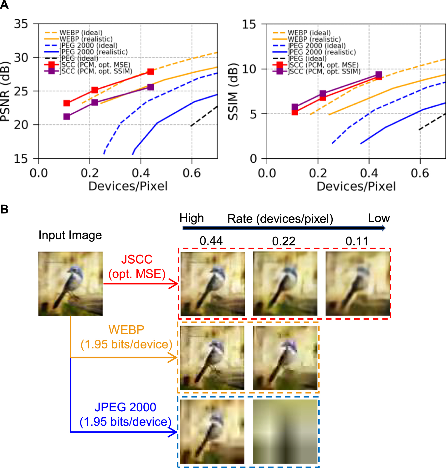
To demonstrate the JSCC scheme, we compressed and stored the 64 × 64-pixel (24-bit depth, 8 bits per pixel per color channel) RGB images onto the PCM array with three different rates (0.11 devices/pixel, 0.22 devices/pixel, 0.44 devices/pixel). The rate is defined as the ratio of the number of cells used to store the image (448, 896, 1792, respectively) to the original image pixel numbers (64 × 64 pixels). Figure 1(D) shows examples of image storage and reconstruction at 0.44 devices/pixel rate. We compared the performance of the JSCC scheme against separate source and channel coding with digital storage. As a baseline for the source coding we used JPEG, JPEG 2000 and WebP [6]. For the PCM digital storage channel, we take the characterized PCM channel capacity 1.95 bits/device as the ideal transmission rate, and 1.35 bits/device as the realistic transmission rate considering MLC storage of PCM protected by industry-standard ECCs (see supplementary text 3 for calculation details). Summarized rate-distortion curves are shown in figure 2(A). Peak signal-to-noise ratio (PSNR, in units of dB,  ) and SSIM (in units of dB,
  value) are used to quantify image distortion. We compressed and stored 100 64 × 64-pixel RGB test natural images with different rates, with each curve representing the average rate-distortion tradeoffs for each method. The results show that JSCC trained with MSE loss is comparable to WebP +1.95 bits/device digital PCM, and outperforms JPEG and JPEG2000 on both metrics, with substantial improvements at lower rates. When measuring distortion with SSIM, JSCC trained to optimize SSIM showed a larger gain. Figure 2(B) shows an example image compressed to similar rate by different methods. As rate is reduced, WebP + 1.95 bits/device digital PCM and JPEG2000 + 1.95 bits/device digital PCM degrade the reconstruction of the original image with generation of virtual artifacts, and would not be able to go down to 0.11 devices/pixel for this 64 × 64-pixel RGB image, while the JSCC scheme gracefully degrades by simply blurring over the details of images and thus achieves a better reconstruction at low rate. We point out that JSCC learned to make good use of the available channel capacity in extended data figure 5.

Figure 2. Competitive performance of JSCC. (A) Rate-distortion curves measured with PSNR and SSIM, averaged over 100 64 × 64-pixel natural RGB images: PCM analog storage with JSCC optimized for MSE (red) and optimized for SSIM (purple); PCM digital storage with JPEG (black), JPEG 2000 (blue), and WEBP (orange). Ideal PCM transmission rate (dashed line) is 1.95 bits/device, realistic PCM transmission rate (solid line) is 1.35 bits/device. JSCC consistently requires less devices/pixel than conventional image codecs to achieve the same PSNR/SSIM index. (B) Example image compressed and stored by different methods, at three different rates; JSCC scheme achieves a better perceptual reconstruction at low rate.
Download figure:
Standard image High-resolution image3. Error-resilience of JSCC to device non-idealities
Historically, the analog approach has been seen as a more efficient path for resource utilization than the digital approach, but at the cost of increased sensitivity to noise and device non-idealities [27]. JSCC solves this tradeoff by transforming the source distribution into a distribution which is 'probabilistically' matched to the channel distribution [28] and thus is robust to small perturbation to the channel characteristics. Here we show that the JSCC scheme is error-resilient to three major PCM device non-idealities: device failure, unseen large variation (ULV), and resistance drift. Device failure can be caused by fabrication yield or limited endurance, when some PCM devices no longer switch and instead become stuck at either the highest (SA1) or lowest (SA0) possible resistance state. ULV happens when some memory cells within a large-scale array behave with a larger device variation than the Gaussian noise term  assumed in training. To test the scheme's resiliency to SA1, various failure rates
  were simulated by randomly selecting a set of cells of the memory array and RESET'ing them to the maximum possible resistance value
  (figure 3(A)),
  . To simulate ULV, we used a Gaussian mixture model combining the characterized channel model and a simulated channel with noise term twice as large,
 ![${\text{R}}\left( i \right) = { }\mu \left( i \right) + \left[ {\left( {1 - \theta } \right)\sigma \left( i \right) + \theta .2\sigma \left( i \right)} \right] \cdot \epsilon ,{ }$](https://content.cld.iop.org/journals/2634-4386/2/4/044018/revision4/nceaca92cieqn21.gif) where
where  and q is the probability of getting data from ULV (figure 3(B)). The reconstruction PSNR and SSIM are averaged over 100 test images for a range of
  and
and  values at different rates. Figures 3(C) and (D) show that the JSCC scheme was able to tolerate up to 0.2% SA1 failure rate and up to 10% ULV cells before suffering noticeable degradation. The resilience to SA0 is slightly better than SA1 (extended data figure 6). Example images stored in a non-ideal array with JSCC are shown in extended data figure 7. By contrast, any single-bit flip not corrected by ECCs in digital storage media would corrupt the reconstructed images using a traditional image codec (see WebP example in extended data figure 8). The relaxation of the amorphous phase of PCM materials will cause the resistance of PCM devices to drift to a higher value after programming [29]. As a result, if we directly put the set of measured resistances Rt
through the decoding network, the reconstructed image will show increasing distortion over time as in figure 3(F) (pink). In fact, drift is a critical reliability issue of PCM devices for both digital and analog applications [30]. Other information storage devices also have similar degradation behaviors although the physical mechanism and time dependence may be different for each type of device. There have been significant efforts expended on mitigating the impact of resistance drift at various abstraction levels [31–35]. Here we use a new algorithm-level method to correct the drift impact on JSCC, with the focus on analog PCM devices where both the stored value and degree of drift are continuous. When decoding the image at time t, we pass the measured Rt
through the drift correction model based on Bayesian statistics (see supplementary text 4 for model details) to infer the initial resistance
values at different rates. Figures 3(C) and (D) show that the JSCC scheme was able to tolerate up to 0.2% SA1 failure rate and up to 10% ULV cells before suffering noticeable degradation. The resilience to SA0 is slightly better than SA1 (extended data figure 6). Example images stored in a non-ideal array with JSCC are shown in extended data figure 7. By contrast, any single-bit flip not corrected by ECCs in digital storage media would corrupt the reconstructed images using a traditional image codec (see WebP example in extended data figure 8). The relaxation of the amorphous phase of PCM materials will cause the resistance of PCM devices to drift to a higher value after programming [29]. As a result, if we directly put the set of measured resistances Rt
through the decoding network, the reconstructed image will show increasing distortion over time as in figure 3(F) (pink). In fact, drift is a critical reliability issue of PCM devices for both digital and analog applications [30]. Other information storage devices also have similar degradation behaviors although the physical mechanism and time dependence may be different for each type of device. There have been significant efforts expended on mitigating the impact of resistance drift at various abstraction levels [31–35]. Here we use a new algorithm-level method to correct the drift impact on JSCC, with the focus on analog PCM devices where both the stored value and degree of drift are continuous. When decoding the image at time t, we pass the measured Rt
through the drift correction model based on Bayesian statistics (see supplementary text 4 for model details) to infer the initial resistance  , and then feed
  into the decoding network to obtain the reconstructed image (figure 3(E)). The reconstruction performance from the inferred case is significantly improved over the direct measured case as seen in figure 3(F) on the timescale measured. At the hardware level, as analog-to-digital conversion (ADC) energy scales up with the ADC resolution [36], we analyzed the impact of reduced precision read and write on our system performance. We show in extended data figure 11 that although quantization is not included during training, a 5-bit precision read and write has a minimal effect on the image storage and retrieval performance for this PCM channel.

Figure 3. Error-resilience of JSCC to PCM device non-idealities. Simulated channel characteristics accounting for (A) stuck at the highest possible resistance state (SA1) failure, (B) unseen large variation (ULV). Reconstruction PSNR and SSIM at various (C) SA1 failure rates p and (D) ULV probability q, with rates of 0.44 (orange), 0.22 (blue) and 0.11 devices/pixel (green). Dotted lines refer to  =
=  = 0. JSCC scheme was able to tolerate up to 0.2% SA1 failure rate and up to 10% ULV cells before suffering noticeable degradation. (E) Measured channel characteristics drift along with time (upper left) and inferred channel characteristics remain stable over time (upper right). (F) Reconstruction PSNR and SSIM decoded at different times from inferred resistance from drift correction model (blue) improved significantly over decoded from resistance measured (pink).
Download figure:
Standard image High-resolution image4. Adaptability of JSCC to different NVM characteristics
Finally, we point out that JSCC can be adapted to different NVM characteristics and benefit from improvement at the device level without extra design effort. To illustrate this, we demonstrate JSCC with a write-verified 1 M-cell 1T1R RRAM array (See RRAM array and characterization details in SI methods).Write-verification is typically employed for today's NVM (e.g. NAND Flash [10]) in mass production to efficiently reduce device variation by iteratively programming-and-verifying the cell value into a desired range. The write-verified RRAM channel model is constructed as:  where
where  is the midpoint value of desired conductance range, and the measured conductance
  for a given
  is modeled as a Gaussian distribution, with mean
  and standard deviation
  given by the mean and standard deviation values extracted from the experimental distributions measured ∼1 min after programming (figure 4(A)) to capture the short-term (∼s) RRAM relaxation [37] effect. Smaller device variation leads to larger channel signal-to-noise ratio (SNR) and thus smaller information loss through signal compression and retrieval by JSCC. The rate-distortion curves in figures 4(B) and (C) show that JSCC with write-verified RRAM results in an immediate gain over the one-shot programmed PCM case, and its performance is consistently comparable with WebP + ideal write-verified RRAM transmission rate at low rates (example images in figure 4(D), additional RRAM results in supplementary text 6, extended data figures 12 and 13).

Figure 4. Adaptivity of JSCC to write-verified 1 M-cell 1T1R RRAM array (A) Write-verified RRAM channel characteristics. GT is target conductance representing the midpoint values of desired ranges (range bounds in green dotted line). GM is corresponding conductance distributions read 1 min after programming plotted as 1-standard deviation error bar. Rate-distortion curves measured with PSNR (B) and with SSIM (C), averaged over 100 64 × 64 pixel test natural images: Write-verified RRAM analog storage with JSCC optimized for MSE (results acquired at ∼ 1 min (dark blue) and ∼ 15 h (light blue) after programming show indistinguishable difference, and therefore the two curves overlap each other) improves over one-shot programmed PCM analog storage with JSCC optimized for MSE (red, inserted figure) because of smaller device variation; Write-verified RRAM digital storage with JPEG (black), JPEG 2000 (blue), and WEBP (orange). Ideal write-verified RRAM transmission rate (dashed line) is 3.82 bits/device, realistic write-verified RRAM transmission rate (solid line) is 2.85 bits/device. JSCC consistently requires less devices/pixel than conventional image codecs to achieve the same PSNR/SSIM index. (D) Example images compressed by different methods: JSCC+ analog write-verified RRAM, JSCC+ analog one-shot programmed PCM, and WEBP+ 3.82 bits/device digital write-verified RRAM.
Download figure:
Standard image High-resolution image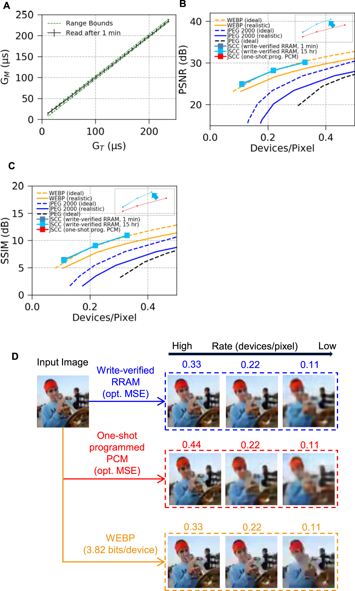
5. Previous work
Our prior work related to the current work are [5, 19, 20], which considered the problem of storing analog signal with analog memory devices, but without large-scale hardware demonstration. To be specific, [5] characterized the channel capacity of a single analog PCM device and showed a way of storing a Gaussian source with a single-symbol analog coding; [19] disclosed the JSCC concept by simulating grey-scale image storage on idealized modeled PCM devices; [20] stored by experiment one gray-level image onto 1 K-cell analog RRAM array with JSCC scheme. The current work presents hardware demonstrations of 100 RGB images storage with JSCC scheme on both large scale (1 M-cell) PCM array and large scale (1 M-cell) RRAM array at different compression ratios, statistically analyses of JSCC experimental performance compared with conventional digital storage of images, and comprehensively investigates the impact of both PCM and RRAM device non-idealities on JSCC performance.
6. Discussion and summary
To conclude, our main contribution is to provide an efficient way to store analog data—which currently is and will likely continue to be a major portion of the world's data streams in coming years—into analog memory devices. The method not only shows competitive performance against traditional image codecs paired with digital data storage at low rate, but also is resilient to analog device non-idealities. Additional challenges will arise when storing images on large-scale NVM arrays with only one-shot programming. Specifically, the further devices from power source will experience weaker programming pulses due to the IR drop and RC delay along with long WL/BL/SLs. This will result in deterministic spatial variations of device characteristics as examples shown in [38]. To compensate for the impact of cell locations, location-aware write schemes such as [39] can adjust the programming pulses based on the cell locations. The results presented in this work should be seen as a starting point, as there is ample room for improvement. For example, one could extend the auto-encoder to learn variable length codes adaptive to image content. Another direction would be fully implementing the JSCC coding network with analog Compute-in-Memory architecture (Extended Data figure 4(B)) based on RRAM/PCM [34, 40] with a careful analysis on analog core SNR in order to achieve more energy-efficient image storage and retrieval. We expect that a combination of these approaches could lead to revolutionary ways of achieving highly compact analog data storage with emerging NVM technologies.
Acknowledgments
This work was supported in part by ASCENT, one of six centers in JUMP, a Semiconductor Research Corporation (SRC) program sponsored by DARPA, the DARPA 3DSoC program, and additionally supported in part by member companies of the Stanford SystemX Alliance and the Non-Volatile Memory Technology Research Initiative (NMTRI). This work was initiated under the SONIC project in STARnet (SRC/DARPA), and received continuing support from an Intel Research gift (B A O). A Levy is supported by NSF graduate research fellowship program.
Data availability statement
All data that support the findings of this study are included within the article (and any supplementary files).
Supplementary data (1.7 MB PDF)