
Abstract
Non-through and through nanopores were introduced to study the Raman band shift of suspended graphene by the substrate edge and the helium ion beam irradiation during the fabrication of nanopore in graphene. Before the ion beam irradiation, there is a blue-shift in the G band and G' band of suspended graphene on the micro-scale non-through and through holes edge because of the n-type mixing for suspended graphene from the translocation. After different doses of the helium ion irradiation, G' band Raman of suspended graphene on through are blue-shift, and the G band positions are red-shift. Helium ion irradiation introduces n-type doping during the graphene nanopore fabrication. The observed Raman shifts help us to gain more intrinsic properties of the graphene nanopore. Thus, Raman spectroscopy can be used as a quantitative diagnostic tool to character graphene-based nanopore.
Export citation and abstract BibTeX RIS

Original content from this work may be used under the terms of the Creative Commons Attribution 4.0 licence. Any further distribution of this work must maintain attribution to the author(s) and the title of the work, journal citation and DOI.
1. Introduction
The study of graphene films has attracted much attention during the past several years due to their excellent mechanical, thermal, electrical, and optical properties [1, 2]. In recent years, graphene nanopore has been identified as a promising structure for gene sequencing at a single-base resolution, and it has been proved in DNA sequencing [3–5]. Graphene nanopore has also been demonstrated potential applications in ion filtration, such as seawater desalination [6, 7]. Besides, the nanomesh structure was created on a supported graphene film, which makes graphene designed for the graphene-based semiconducting film device [8]. Thus, exploring efficient graphene nanopore fabrication and characterization technology is of vital importance for graphene-based devices.
Nowadays, the research demonstrated that a focused electron beam and focused ion beam can be used to fabricate nanopore from several nanometers to tens of nanometers [9–11], and it is still the most effective method for the preparation of graphene nanopore [11, 12]. However, ion beam irradiation has a great influence on the intrinsic properties of films during the fabrication of graphene nanopore [13–16]. Raman spectroscopy provides a powerful tool to study the properties of graphene irradiated with an ion beam [17–19]. The Raman spectra of graphene are mainly characterized by three prominent feature peaks associated with the D band (1350 cm−1), G band (1580 cm−1), and G' band (2690 cm−1). The D band is typically utilized to characterize the lattice damage in graphene. The G band is attributed to the bond stretching of the pairs of sp2 carbon atoms. The G' band corresponds to the high-energy second-order process. The shape of the G' band and the ratio of intensity between the G band and G' band are used to identify the number of graphene layers. The intensity ratio of the defect-induced D band to the first-order G band, ID/IG, provides a spectroscopy-based method to quantify the defect density of graphene [20, 21]. Recent study shows that the built-in stresses provide the energy for defect propagation in stretch graphene film. Thus, the intensity ratio of ID/IG increases with the Raman test point approaching the substrate edge [22]. However, there are few studies on the helium ions bombed, and the substrate edge induced defects and dopants change on suspended graphene.
It is important to study the properties of graphene on a suspended substrate, and non-through and through nanopores were introduced to this study. This work presents the evolution of Raman spectra of D, G, and G' modes for suspended graphene before and after helium ion irradiation. By analyzing the behavior of these Raman band frequency and intensity with the change of substrate edge and helium ion irradiation. It is shown that a signature of a blue-shift in the G band and G' band for substrate edge graphene film before the ion bomb. After the helium ion irradiation, the G' band Raman of suspended graphene on through are blue-shift, and the G band position is red-shift. Helium ion irradiation introduces hole and n-type doping during the graphene nanopore fabrication [23]. These results provide fundamental information about the lattice structure change during the helium ions irradiation, which is useful for graphene nanopore fabrication.
2. Methods
2.1. Holey silicon nitride substrate preparation
The 20 μm × 20 μm freestanding silicon nitride (SiNx) membrane supported on 400 μm thick silicon (100) substrate with the thickness of 20 nm was created by conventional optical photolithography followed by anisotropic wet etching of silicon in KOH solution. Then, the holey SiNx with a diameter of 1 μm wells array was fabricated through the gallium ion (Ga+) focused ion beam (FIB) technology with an acceleration voltage of 30 kV. The Ga+ ion beam current was about 6 pA and the beam does was 0.3 nc μm−2.
2.2. Suspended graphene sample preparation
Graphene sample was obtained grown by large area (14 inches) grown method through chemical vapor deposition (CVD) technology on a Cu foil. Then cut it into small pieces (0.5 cm × 0.5 cm) and transferred it to the prepared holey SiNX substrate by the PMMA assistant wet transfer. The poly(methyl-methacrylate) PMMA layer about 200 nm was spin-coated onto the sample. The Cu foil was etched away with ammonium persulfate ((NH4)2S2O8). The sample was then transferred into fresh DI water. Then, the sample was taken out of the DI water slowly with the holey SiNx substrate and heated on a hot plate at 150 ℃ for ∼20 min to make better adhesion to the substrate. The graphene/PMMA layers were transferred to the SiNx membrane. Finally, the PMMA layer was dissolved in the acetone and then heated on the hot plate at 150 ℃ for ∼5 min to evaporate residual solvents.
2.3. Graphene nanopore fabrication
Graphene nanopore fabrication by a focused helium ion beam under the pressure of 1 × 10⁻⁷ Torr and ion beam current of 0.10 pA at 10 μm aperture size based on helium ion microscopy (HIM, Zeiss Orion Nano Fab). Two low beam doses (8 × 10⁴ ions, 1 × 10⁵ ions) and two high doses (6.5 × 10⁵ ions, 7.5 × 10⁵ ions) were used to fabricate graphene nanopore.
2.4. Raman spectroscopy
Raman spectra of graphene were acquired under ambient conditions with a Renishaw confocal micro Raman microscope equipped with a 532 nm laser. A 100× objective lens and a diffraction grating with 1200 lines mm−1 were used. The spatial resolution of the laser was ∼0.76 μm. A 1 s acquisition time and four spectrum averages were used at each point. Unless otherwise specified, the integration time was 1 s, the number of acquisitions was 1 time, and the laser power on the sample was about 2 mW for each Raman measurement. The most prominent features of the Raman spectrum of graphene are the characteristic G band at ∼1580 cm−1 and the G' band at ∼2700 cm−1. A third band, the D band at ∼1350 nm−1, becomes Raman active in defective graphene.
3. Results and discussion
3.1. Raman spectroscopy of continuous suspended graphene film
The setup of the suspended graphene film sample was shown in figure 1(A). At first, 4 through holes with a diameter of 1 μm and a non-through hole were drilled on the SiNX window using a focused ion beam (FIB). Based on PMMA assistant wet transfer method, the monolayer graphene film was transferred onto the patterned SiNx substrate. The FIB and optical image of the prepared SiNX holes as shown in figures 1(B), (C). Then, the PMMA was removed cleanly from the graphene film for the next experiment, and the continuous suspended graphene film was obtained. Figure 1(D) is the optical image of the SiNX holes with graphene film. After the PMMA layer was removed, the graphene edges could be clearly identified on the SiNx surface [24]. The insert in figure 1(D) shows that the PMMA was removed cleanly from the graphene film. Next, the suspended graphene nanopores were prepared on the SiNx holes by optimizing the aperture and beam current of the helium ion microscope based on focused helium ion etching technology.
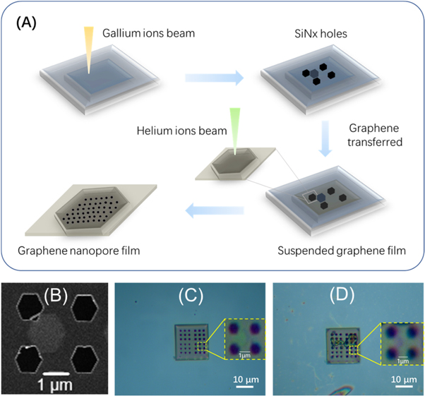
Figure 1. (A) The scheme of the setup of suspended graphene film; the FIB image (B) and the optical image of SiNx holes (C); the optical image of the graphene film (D).
Download figure:
Standard image High-resolution imageTo get the transferred graphene film information, Raman measurements were performed for the unirradiated graphene film. Figure 2(A) demonstrated the experimental setup for the suspended and supported film. There are two strong Raman bands for this unirradiated suspended and supported graphene film as shown in figure 2(B). The G band (∼1580 cm−1) is generated from in-plane sp2 C–C stretching mode. The G' band, (∼2700 cm−1), which is a second-order Raman process originating from the in-plane breathing-like mode of the carbon rings. Another important band of graphene is the D band (∼1350 cm−1), which is arising from the breathing modes of six-atom rings and requires a defect for its activation [20, 21]. All the Raman spectra show a sharp single Lorentzian profile for G bands, the G' to G peak intensity ratio (IG'/IG) over than 1, and the D bands are very low. These results indicated that the presence of the transferred graphene film is a single layer and there is no obvious defect [25]. However, the Raman spectral for suspended and supported graphene film is different. These changes are probably come from the effect of the substrate. Furthermore, the non-through hole was introduced for the further investigation of the substrate effect on suspended graphene. As shown in figure 2(B), the Raman intensity of suspended graphene film are higher than the supported film. Take the G' band, for example, the intensity of graphene on the through-hole (c) shows 3 times compared to the graphene on the non-through hole (b), and 9 times for the supported graphene (a). It also demonstrates that the defect-related D band intensity of monolayer graphene on the non-thorough hole is obviously enhanced compared to those on SiNx and thorough holes. This result may attribute to the large area of the non-through hole. The monolayer graphene film couldn't be suspended very well on such a large hole, and introduce some defects. Besides, figure S1 (available online at stacks.iop.org/NANOX/2/010001/mmedia) shows the intensity of the G band and G' band mapping of the continuous suspended graphene film. The previous studies on the stress effect of the monolayer graphene film show that the G' band intensity can increase with the tensile strain [26].

Figure 2. (A) Schematics of the experimental setup for suspended and supported film; (B) Raman spectra of the continuous graphene monolayer film supported on the SiNx (a), suspended on the non-through hole(b) and through-hole(c) respectively; Raman mapping (scanning step: 0.5 μm) of the G band position (C), and G' band position (D). The yellow dash ranges are through holes, the green dash range is the non-through hole.
Download figure:
Standard image High-resolution imageFigures 2(C), (D) shows the Raman mapping results of the G band and the G' band Raman shifts of the continuous graphene film on the SiNx holes array. The yellow dash ranges are through holes, the green dash range is the non-through hole. The zone-center LO phonon around 1580 cm−1 (G band) and the two-phonon peak around 2700 cm−1 (G' band). The phonon frequencies of graphene might be influenced by mechanical strain and charge [27–29]. Raman spectra and the peak fitting of different locations are shown in figures S2(A), (B). These results show that the G band is 1591 cm−1 and G' band is 2683 cm−1 on the SiNx substrate. According to the previous report, the impurities in the substrate and the surrounding environment would lead to Raman band shift. Water and oxygen molecules absorbed on the graphene surface can introduce a p-type dopant, resulting in a blue-shift [29]. For the through-hole, compared with the Raman shift of graphene on a substrate, both G and G' bands of monolayer graphene on hole edge red-shift with the shift of 3 and 9 cm−1, respectively. In the center of the suspended area, the G' band is shift back, and G band shows a blue-shift (3 cm−1) compared with the graphene on the substrate. As for the non-through hole, it is almost the same phenomenon as the through-hole. Compared with graphene on the substrate, both G and G' bands of monolayer graphene on non-through hole edge show red-shift (5 cm−1, 5 cm−1). In the center of the suspended area, both G and G' bands are blue shift with 4 and 7 cm−1, respectively. These results show that the shift of G' band is much larger than that of G band. The redshift of the Raman Band can be attributed to the stretching of the carbon-carbon bond [30]. It is reported that no matter n-type or p-type, the G band position of single-layer graphene shifts to a higher wave position with the weakening of the Kohn anomaly effect. The G band shifts to the low wave when the n-type is mixed [31]. Thus, these phenomena also indicated that the substrate of the substrate edge may introduce n-type mixing for suspended graphene approaching the substrate edge.
3.2. Helium ion does effect on suspended graphene nanopore
The suspended graphene nanopores were prepared on the SiNx through wells by optimizing the aperture and beam current of helium ion microscope based on focused helium ion etching technology. First, the 10 μm through holes were selected, and the helium ion beam current is about 1.5 pA at the pressure of 1 × 10⁻⁶ Torr. Then, according to our early work [12], two low beam doses ( 8 × 10⁴, 1 × 10⁵ ions) and two higher doses (6.5 × 10⁵, 7.5 × 10⁵ ions) were set to study the helium ions influences on suspended graphene film during the fabrication of graphene nanopore. The non-through hole didn't irradiate for the control experiment.
Figure 3(A) shows the Raman spectral of the helium ion treated of suspended graphene film on SiNx through wells. Raman defect-induced D and D' bands in defective monolayer graphene appear at 1350 and 1620 cm−1, respectively. The D band requires a defect for its activation and originating from the breathing modes of six-atom rings and requires defect for its activation.

Figure 3. (A) Raman spectra of suspended monolayer graphene exposed to helium beam with distinct ion doses. (B) The intensity ID/IG and IG'/IG change with distinct Helium ion doses, respectively. (C) Optical image of the Raman spectra mapping area. Raman spectra mapping of graphene nanopore film under helium ion beam for the G' band intensity (D), G' band intensity (E). The yellow dash ranges are through holes, the green dash range is the non-through hole.
Download figure:
Standard image High-resolution imageThe defect density of graphene can be quantified by measuring the intensity ratio (ID/IG) of the D and G band. Figure 3(B), shows the relationship between Raman intensity ratio of ID/IG , IG'/IG, and irradiation dose. With the increase of helium ion does, the IG'/IG of suspended graphene decrease gradually. However, the intensity ratio of ID/IG increases with the dose at first, and then down to 1.5 when the irritation dose at 7.5 × 10⁵ ions. It demonstrated that the trend of defect ID/IG ratio of graphene monolayer doesn't simply change with the increase of the dose of the helium ion beam. This phenomenon evidences the evolution of disordered graphene from graphite to nanocrystalline graphite [32–34]. Although the FIB imaging (figure S3) of graphene nanopore array changes obviously with the increase of the helium ion dose. Since ID/IG intensity ratio does not depend on the geometry of the defects, the intensity ratio between the D and D' can be used to characterize defect types [35]. ID/ID' ratios measured in a range of 1.9–2.5, which are smaller than those for point defects [36], and show an increase with an increase of the irritation dose (figure 4(A)). Raman mapping has been done to directly probe the change with the helium doses irritation. Figure 3(C) shows the Optical image of the Raman spectra mapping area. The yellow dash ranges are through holes, the green dash range is the non-through hole. Figures 3(D), (E) shows the Raman mapping results of the G band and G' band Raman shifts of graphene film on the SiNx holes array after the helium doses irradiation. Raman spectra and the peak fitting of different locations are shown in figures S2(C), (D).

Figure 4. The ID/ID' ratio (A), plot of G (B) and G' (C) peak position change with distinct Helium ion.
Download figure:
Standard image High-resolution image
The G band and G' band peak position of graphene on the substrate are 1596 and 2686 cm−1. After the ion irritation, the Raman showed a blue-shift with a shift of 5 and 3 cm−1, which are compared to the untreated graphene film on the substrate. This phenomenon has also been confirmed by the other location graphene film (on through hole edge, non-through hole edge, suspended on the non-through hole), where are undirectly bombed by helium ions. Compared with the same location untreated graphene, the Raman shifts of all the undirectly bombed graphene are bule-shift. It has been reported that the G band peak position increases as a function of both electron and hole doping. The blue-shifted G' peak position observed in graphene is attributed to unintentional doping in graphene by the charge impurities present on the SiNx substrate [34]. As for the helium ions directly irritated graphene film, take the irritation dose at 7.5 × 10⁵ ions (i) for example. Compared with the Raman shift of graphene on this substrated, all of the D, G and G' bands peak position of the suspended graphene are red-shift with the shift of 5, 6, 10 cm−1, respectively. As shown in figure 4(B), the G band always around 1590 cm−1 under different helium does irrational. The G' mode shifts almost linearly with the increase of irritation dose in a range of 2673–2677 cm−1 (figure 4(C)). The G frequency shift is similar to the doping effects, which is may due to the He+ irradiation of graphene on SiNx substrate introduce n-type doping. That is to say, with the He+ irradiation dose increase the hole and n-type doping are increased. Besides, the G' band shift range of the helium ions bombed suspended graphene is much smaller than the untreated suspended graphene. These results may due to the removal of water and oxygen molecules adsorbed on graphene during the fabrication of nanopore in suspended graphene.
4. Conclusion
This work studies the Raman spectral of suspended graphene impacted by the wells edge and the helium ion beam irradiation during the fabrication of nanopore in graphene. Before the ion beam irradiation, the Raman intensity of suspended monolayer graphene film on through hole higher than the non-through and supported graphene film thanks to the stress effect. Compared to Raman peak position of graphene on substrate, there is a red-shift in the G band and G' band of suspended graphene on the micro-scale non-through and through holes edge due to the substrate introduced n-type doping. After different doses of the helium ion irradiation, Compared to Raman peak position of untreated suspended graphene on through hole, both G band and G' band Raman of suspended graphene on through holes are red-shift. These results may due to the removal of water and oxygen molecules adsorbed on graphene during the fabrication of nanopore in suspended graphene. With the increasing of helium ion dose, the G' mode shifts increased linearly, the peak position of G mode almost don't change. These results may due to the He+ irradiation of graphene on SiNx substrate introduce n-type doping.
It demonstrates that with the He+ irradiation dose increase the n-type doping is increased. The observed Raman shifts help us to gain more intrinsic properties of the graphene nanopore. These results are useful for assessing the utility of regularly patterned graphene nanostructures and engineering graphene-based electronic devices upon the introduction of defects.
Acknowledgments
This work was supported by the Youth Innovation Foundation of CIGIT; Naturak Science Foundation of Chongqing: cstc2018jcyjAX0308, cstc2018jcyjAX0310; Instrument development program of CAS:YZ201568; Chongqing Talents: CQYC201905007; Youuth Innovation Promoion Association of CAS:2017392.