
Abstract
In this paper, a 128-channel non-uniform optical phased array is proposed. The antenna is based on a silicon nitride waveguide with a large cross-sectional area (3 μm × 1.2 μm) and a silicon nitride grating with a small diffraction window (grating width of 200 nm), enabling high optical power transmission and a wide 1 dB field of view. As a result, the designed sparse optical phased array achieves less than 1 dB of main lobe attenuation over a 94° field of view. Within this field of view, the main lobe will not fall below 80% of the maximum main lobe. This allows the minimum detection distance to still be about 89% of the maximum detection distance without increasing the input power. In this field of view, the maximum side-lobe suppression of the designed sparse optical phased array is 13.4 dB, and the minimum side-lobe suppression is higher than 11.9 dB. This is useful for simultaneously achieving a large field of view, low main lobe attenuation, stable side-lobe suppression, and long detection distance.
Export citation and abstract BibTeX RIS
1. Introduction
Researches of LIDAR based on on-chip integrated optical phased arrays are increasing. Several research teams have conducted related chip detection studies and made exciting progress [1–4]. According to the lidar ranging equation [5], the relationship between emission optical power and detectable distance is represented by P1/P0∝1/D2, where P1 represents the power of the received reflected light, P0 is the optical power of the emitted light (main-lobe), and D is the detection distance. The MIT team achieved detection of a 10% reflective object at a distance of 35 m using 50 mW of main lobe optical power [3]. According to the equation, a W-class main lobe optical power will be required when the detectable distance increases to 200 m. Silicon nitride waveguides have low loss and can withstand high optical power, which is conducive to increasing the optical phased array(OPA) main lobe power [6, 7]. However, the overall loss of the chip may require high input optical power [1]. For example, with a main lobe power requirement of 1 W and a chip loss of 15 dB, the input power will need to be 45 dBm. Therefore, silicon nitride waveguides with large cross-sectional area may have a good potential when the chip insertion loss is large.
However, large cross-section waveguides imply large array spacing, which means that sparse array design is required to achieve a large field of view(FOV). In 2016, Intel's team achieved a scanned field of view of 80° with a sparse array optical phased array [8]. However, limited by the width of the diffraction spectrum of the single antenna, the intensity of the main lobe at the edge of the field of view will be reduced to half of its maximum value. In 2022, Kunyang Du et al improved the fitness function for optimised sparse arrays, which can achieve a 14 dB side-lobe suppression(SSR) over a range of 120° considering only the array factor [9]. However, they were only able to obtain a SSR higher than 11 dB at 80° with the addition of the antenna diffraction factor. There are many studies of sparse arrays [10–18]. Some have considered only the array factor and obtained large fields of view and high side-mode rejection ratios [11, 13–15, 17]. Some have fabricated chips and demonstrated a large field of view, but only the intensities normalised separately for different scanning angles are shown, not the intensity normalised to the maximum principal flap intensity [16, 18].
In this article, we design a 128-channel nonuniform optical phased array. It is based on a thick silicon nitride platform with a waveguide cross-section of 3 μm × 1.2 μm, which allows transmission of higher optical power. Afterwards, the effect of different grating widths on the diffraction spectrum of a single antenna is analyzed, and a grating width of 200 nm gives a diffraction spectrum width of 97.2° of 1 dB (~80%). Then the pitches of adjacent channels of the 128-channel non-uniform optical phased array are optimized by genetic algorithm. Finally, Finite difference time domainmethod(FDTD) simulation is performed based on the 128-channel pitch results, and the 1dB field of view of 94° is obtained for this optical phased array. In this field of view, the SSR is over 11.9 dB and the minimum detection distance can still reach about 89% of the maximum detection distance according to the lidar ranging equation.
2. Simulation and analysis
Firstly, the factors affecting the diffraction field of a single antenna are analyzed. The optical antenna is formed by fabricating a grating on the waveguide and coupling the guiding mode to the radiating mode by perturbing the waveguide through the grating (figure 1). The grating width is Wgs, the grating length is Lgs, the grating period is P, the waveguide width is Wg, the waveguide thickness is Hg, and the spacing between the waveguide and grating is Gap.
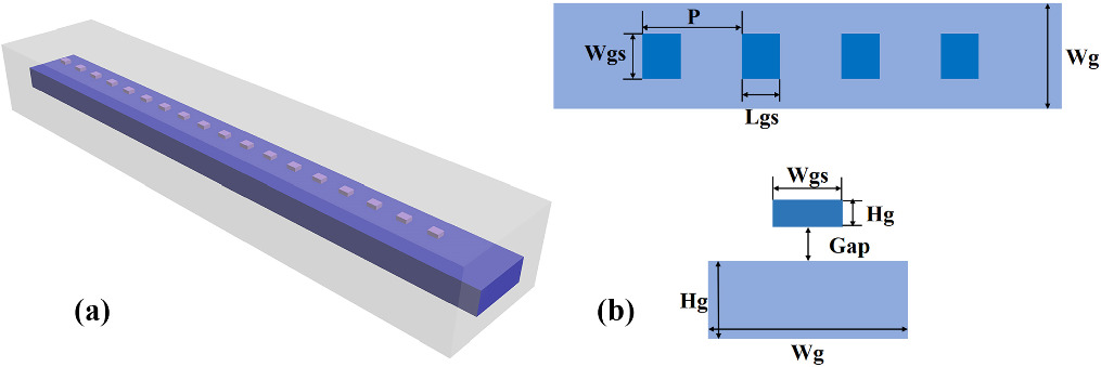
Figure 1. (a) and (b) Antenna structure.
Download figure:
Standard image High-resolution imageThe grating is equivalent to a diffraction window in the waveguide. Here, a rectangular surface grating is used. Approximate grating diffraction Pfar as moment-hole diffraction:

where α = k·a·sinθx/2 and β = k·b·sinθy/2, k is the wave vector, a is the grating width and b is the grating length. fa and fb denote the limits of the width and length of the grating on the diffracted field distribution in the θx and θy axes, respectively. A single antenna consists of gratings arranged periodically along the waveguide. Its far-field derivation process is the same as that of the Fraunhofer multislit interference, but does not satisfy b » a, so the far-field of the single antenna Pfar is:

where δ grate is the phase difference created when light passes through the grating, N is the number of gratings. The far field of an optical phased array is again obtained based on superimposed interference of the far field of a single antenna Pfar:

where δ array is the phase difference between neighbouring channels, M is the number of channels. This suggests that the main flap intensity decay of an optical phased array in the phase-controlled scanning direction is mainly affected by the grating width. Therefore, we fixed the parameters of the antenna and analysed only the effect of grating width on the field of view.
The impact of grating width on the diffraction spectrum of single antenna is illustrated in figures 2(a)–(b). The wavelength is 1550 nm. The grating width (Wgs) is incrementally increased from 100 nm to 2000 nm in intervals of 100 nm. With the increase in grating width, the 1 dB spectral width of the single antenna diffraction spectrum reduces from 97.2° to 21.4°. The desired grating width for obtaining a wide 1 dB single antenna diffraction spectrum is set at 200 nm. This shows that the antenna diffraction spectrum can be effectively extended by reducing the antenna width.
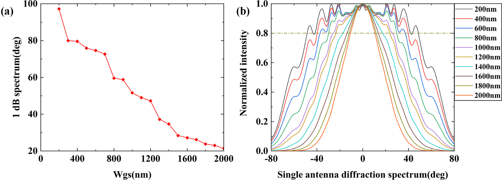
Figure 2. (a) Single-antenna 1 dB (~80%) diffraction spectrum width with grating width (Wgs). (b) Single-antenna diffraction spectrum with different grating widths (Wgs).
Download figure:
Standard image High-resolution imageAs the grating width decreases, the single-antenna diffraction spectrum broadens, and the intensity distribution gradually deviates from the Gaussian distribution spectrum (figure 2(b)). The splitting of the antenna diffraction spectrum from single to multiple peaks as the grating width narrows is thought to be related to swift waves outside the waveguide. In the moment-hole diffraction model, the electric field outside the diffraction hole is zero, and the electric field strength inside the diffraction hole is uniform. Grating diffraction does not satisfy these two limitations.
From equation (3), the grating acts as a diffraction window on the waveguide, and the far-field diffraction spectrum of the single antenna broadens as the grating width decreases. The diffracted field from the grating can be divided into Ex, Ey and Ez components. The input TE0 propagates along the x-axis in the waveguide and diffracts into free space after encountering the grating. Figure 3 compares the diffracted field components Ey of a 200 nm wide grating with that of a 2000 nm wide grating. it can be obtained that the light field limiting effect of the grating on the y-axis is enhanced when the grating width is increased. The intensity of the y-axis component of the grating diffraction field is weakened, and the light intensity is more restricted to a smaller divergence angle. The decrease in the divergence angle of the grating diffraction field leads to the narrowing of the single antenna diffraction field with increasing grating width in figure 2.
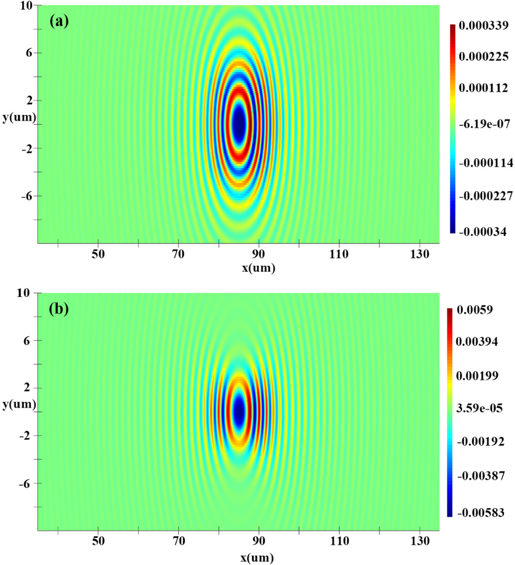
Figure 3. (a) Ey of Single grating (Wgs = 200 nm). (b) Ey of Single grating (Wgs = 2000 nm).
Download figure:
Standard image High-resolution imageFor a wide grating, its width can cover a large part of Ey, with sufficient confining power on the y-axis for the mode field. Similar to the ridge waveguide, the grating is wide enough to focus the light well, limiting the intensity of the mode field component of the diffracted light in the y-axis. When the grating width is reduced to the point where it cannot effectively confine Ey, the grating can no longer serve to focus the diffracted field. At this point the light leaks along the ±y-axis interface of the grating. In this case, the diffracted light produced by the diffracted field separated by the grating toward the +y and -y directions shows the splitting trend in figure 4(b).
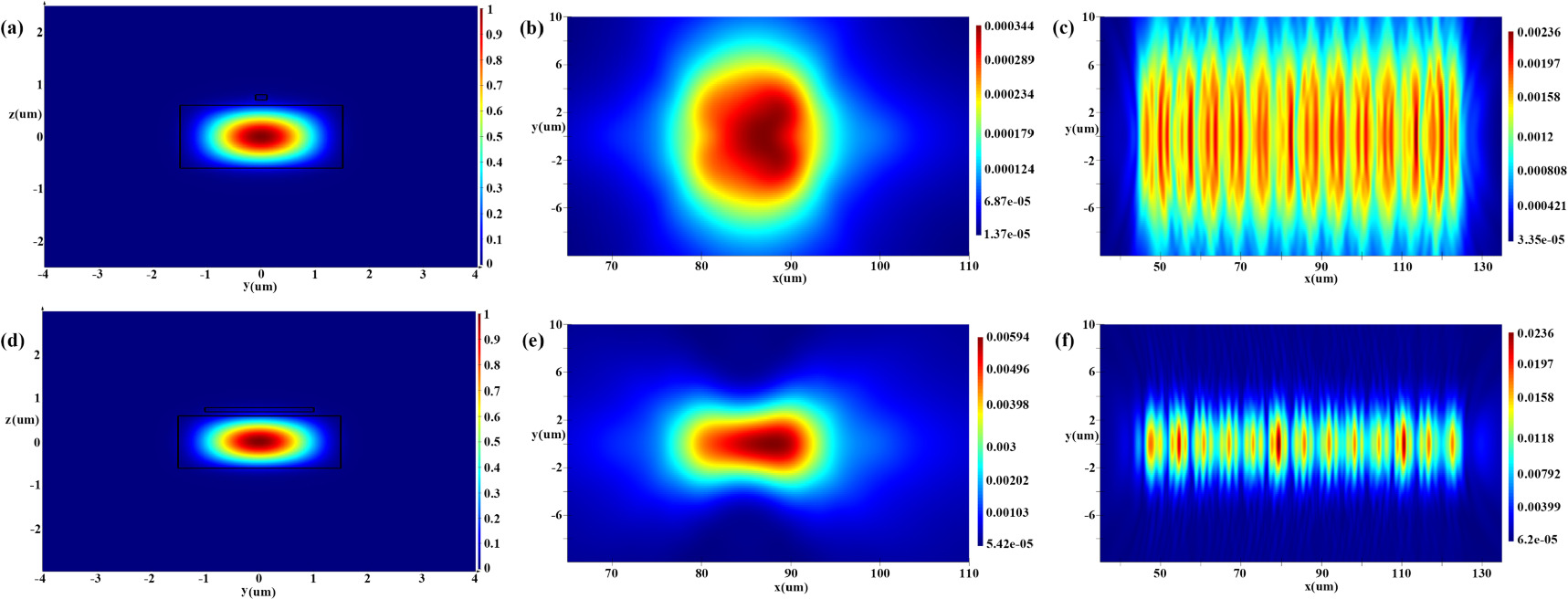
Figure 4. (a) Cross-sectional mode field at Wgs = 200 nm. (b) Near field of Single grating (Wgs = 200 nm). (c) Near field of 100 gratings (Wgs = 200 nm). (d) Cross-sectional mode field at Wgs = 2000 nm. (e) Near field of Single grating (Wgs = 2000 nm). (f) Near field of 100 gratings (Wgs = 2000 nm).
Download figure:
Standard image High-resolution imageWide gratings benefit from a strong light-limiting effect, with Ey focused near the center of the grating, which produces diffraction mainly at the interface of the grating's z-axis and less at the interface of the ±y-axis. In this case, as shown in figure 4(e), the diffracted field produced by the 2000 nm wide grating is a single-peak distribution and does not show a tendency to split. Therefore, as shown in figure 4(c), after the diffracted field of 100 gratings is superimposed, the field obtained from the superposition of 200 nm wide gratings appears to have a multi-peak intensity distribution on the y-axis. And in figure 4(f), the field obtained from the 2000 nm grating superposition still maintains a single-peak intensity distribution on the y-axis. The intensity distribution of multiple peaks leads to a multi-peak split in the far field of the single antenna.
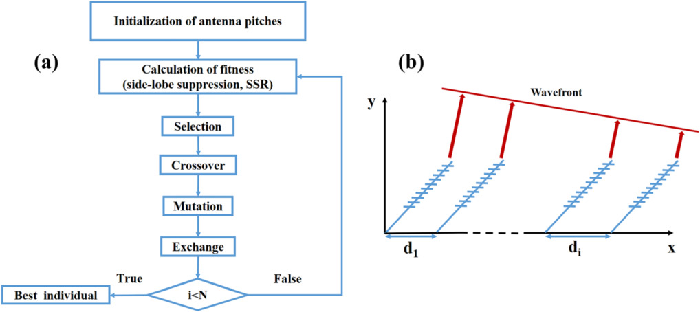
Figure 5. (a) Genetic algorithm. (b) 1D linear array OPA illustration.
Download figure:
Standard image High-resolution imageThen we conducted an optimization on the pitch between the centers of adjacent array elements of a 128-channel optical phased array using a genetic algorithm (figure 5). The far field of the sparse array is:

where Am is the amplitude of the mth antenna and di is the spacing between the i-1th and ith antennas, θs is the main lobe steering angle. The processes of genetic algorithms used in these efforts include population initialization, natural selection, chromosome crossover, mutation, and termination judgments. With reference to mitosis in which chromosomes are pulled equally and randomly into the two cells formed by division, we added the step of exchanging chromosomes after gene mutation. The side lobe suppression as fitness is:

It is usually assumed that Am = 1 and θs = 0. The far field obtained is without the single antenna diffraction factor. Limited by the computational capacity, we can only perform the simulation of FDTD with the maximum single item size of mm level. Therefore, only 128-channel optical phased arrays can be optimized. We performed 50 iterations with a population size of 50 to optimize the pitch for 128 array elements. The spacing of the antennas was limited to 5 μm to 10 μm. Figure 6(a) illustrates the optimized antenna pitches obtained through the genetic algorithm. Based on these optimization results, we achieved a SSR of 13.4 dB at 0°.
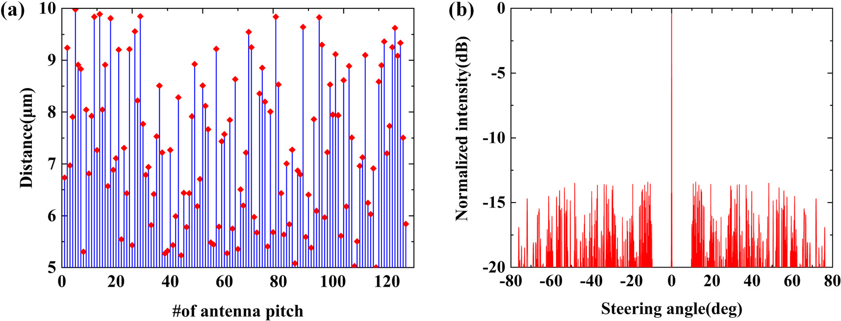
Figure 6. (a) Antenna array pitches. (b) Far field at 0°.
Download figure:
Standard image High-resolution imageFinally, the far-field simulation of the 128-channel optical phased array is conducted using FDTD with antenna. The simulation results are presented in figure 7. The OPA far field obtained by FDTD is limited by the element factor of the single antenna. The attenuation of the main lobe intensity with steering angle has a similar pattern to the intensity distribution of the diffracted field of a single antenna. This suggests that the main lobe attenuation during optical phased array scanning can be influenced by controlling the width of the grating diffraction aperture.
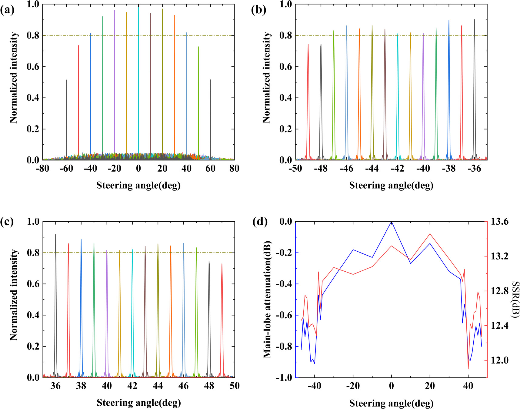
Figure 7. (a) 128-channel non-uniform optical phased array far field. (b) Far field within −50° to −35°. (c) Far field within 35° to 50°. (d) SSR and main-lobe attenuation within −47° to 47°.
Download figure:
Standard image High-resolution imageIt can be observed that the main-lobe intensity of this optical phased array can still reach 80% of the maximum value at ±47° (94°). And the main-lobe attenuation is less than 1 dB. Additionally, within this FOV, the optical phased array exhibits a maximum SSR of 13.46 dB, and a minimum SSR of 11.9 dB. It can be inferred that the designed optical phased array possesses a consistent level of bottom noise within its operational FOV, which facilitates noise processing.
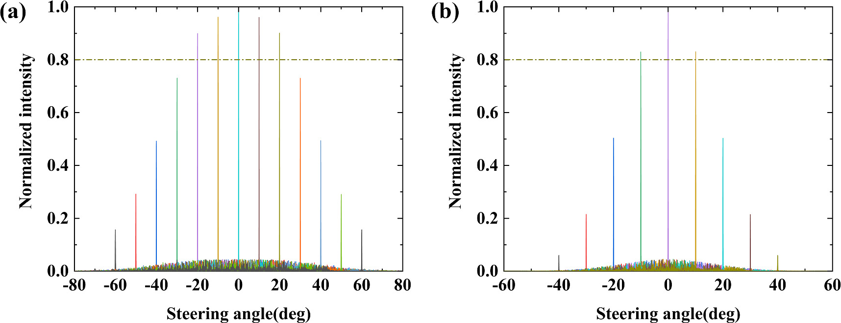
Figure 8 shows the far field of the designed optical phased array when the grating width is 1000 nm and 2000 nm respectively. It can be seen that when the grating width increases to 1000 nm, the optical phased array 1dB main lobe attenuation field of view can only exceed ± 20°, as well as within ± 40° to maintain the main lobe attenuation of no more than 3dB. when the grating width increases to 2000 nm, the optical phased array 1 dB main lobe attenuation of the field of view can only exceed ± 10°, and 3 dB main lobe attenuation can only be up to the range of ± 20°. This demonstrates the helpfulness of reducing the grating width to achieve a large field of view with low main lobe attenuation.
Figure 8. (a) Far field at grating width of 1000 nm. (b) Far field at grating width of 2000 nm.
Download figure:
Standard image High-resolution image
3. Conclusions
We proposed a 128-channel non-uniform optical phased array based on thick silicon nitride waveguides and small-size silicon nitride gratings. The 3 μm × 1.2 μm waveguide cross-sectional area can withstand tens of dBm of transmitted power. By reducing the grating width to 200 nm, the 1 dB diffraction spectrum of single antenna can reach 97.2°. Through genetic algorithm optimization, antenna pitches are determined. The optical phased array achieves a 1 dB field of view of 94°. In this field of view, the SSR is higher than 11.9 dB, and the main lobe attenuation is less than 1 dB. The low main lobe attenuation provides a stable distance detection range, and the minimum detection distance in the field of view will not be less than 89% of the maximum detection distance.
Acknowledgments
This work was supported in part by National Key R&D Program of China under Grants 2022YFB2804503, and in part by the National Natural Science Foundation of China under Grants 62090053, 61934007, and 62105324.
Data availability statement
The data cannot be made publicly available upon publication because they are owned by a third party and the terms of use prevent public distribution. The data that support the findings of this study are available upon reasonable request from the authors.