
Abstract
This study presents an experimental investigation into the solar performance of copper oxide (CuO) thin films. These CuO films were fabricated using the spray pyrolysis technique, and their structural, morpholigical, optical, and electrical properties were examined in relation to the effect of layer thickness. Additionally, we employed SCAPS-1D software to perform numerical simulations of CuO-based solar cells. Moreover, the band gap energy was discovered to be between 1.14 eV, 1.53 eV and 1.61. Using the four-point probe, the electrical resistivity was computed and the high conductivity found corresponds to the sample generated with a film thickness of t = 292 nm, is 7.52 (×10−3 Ω.cm)−1. The CuO/TiO2/FTO solar cell configuration showed a potential efficiency of 13.38% when the absorber layer thickness is 292 nm and the band gap value is 1.53 eV. Furthermore, based on the band gap energy value of 1.53 eV the investigation has been deepened by expanding the range of absorber layer thickness and temperature to thoroughly examine their impact on solar cell performance. Moreover, the CuO/TiO2 solar cells curves of external quantum efficiency (EQE) for various CuO layer thicknesses were determined.
Export citation and abstract BibTeX RIS
1. Introduction
Recently, the scientific community gives great attention to develop copper oxide (CuO) thin films semiconductor to be used in optoelectronics devices may because of the electronical and optical properties [1]. It is a selective metal oxide for many applications such as photocatalytic reactions, semiconductors, gas sensors, batteries, field emission emitters, and photovoltaic cells [2–4]. Due to copper vacancies, which cause the presence of an acceptor level CuO semiconductor possessing an energy band gap of 1.2–2.1 eV [5], monoclinic structure, and p-type conductivity. In addition, the metal oxide CuO is also a transional metal oxide, non-toxic, widely available, and reasonably priced [6]. Moreover, with a single junction solar cell and a CuO band gap value of 1.4 eV, the solar conversion efficiency was found to be 33% in theory [7]. According to the experimental findings, CuO/Si-based heterojunction PV cells' conversion efficiency achieve 0.41% [8].
There is several methods used to elaborate CuO thin films such as sol–gel techniques [9], Spray pyrolysis [10], RF Magnetron Sputtering [11], Chemical Solution Deposition (CSD) method [12], Pulse laser [13] and sequential ionic layer [14].
In the same context, Solar cells have been simulated numerically using the Solar Cell Capacitance Program (SCAPS-1D) for a variety of solar cell architectures, including CdS/CdTe solar cells [15], CdTe and Cu(In, Ga)Se2 solar cells [16], n-TiO2/p-CuO [17] and n-TiO2/p-Cu2O heterojunction solar cells [18]. In 2022, the reported power conversion efficiency of the n-TiO2/p-CuO structured photovoltaic cell by numerical analysis is about 19.42% [19]A conversion efficiency of 18.63% was reported for the n-TiO2/p-CuO structure photovoltaic solar cell founded by Babu et al [20].
In this paper, Spray pyrolysis will be used to produce CuO thin films because it's simple and low cost method, aiming to study the impact of thin film thickness on optical, structural and electrical properties of CuO thin films for application on PV cells. SCAPS-1D programs used to simulate a solar cell based on CuO/TiO2 as well as to assess how the temperature and film thickness affect the properties of solar cells.
2. Materials and methods
2.1. Experimental procedure
Spray pyrolysis was used to prepare CuO thin films, (CuCl2, H2O) as a precursor, it was dissolved in 15 ml, 20 ml and 25 ml of distilled water. Just before deposition, ethanol and distilled water were applied to the glass substrates to clean them of any impurities or contaminants. The concentration solution is 0.2 M and it was stirring for 15 min, that one was manually applied to the 300 °C preheated glass substrate using a scented atomizer. Besides that, Thermal treatment was applied to the resulting sprayed films for 1 h at 300 °C Then, after this reaction, the creation of the CuO thin films begins [10]:

All other parameters were maintained, and we merely changed the volume of the sprayed solution in order to change the thickness of CuO thin films.
2.2. Numerical simulation study
Over the past few decades, the simulation tool or software has been increasingly important and necessary, especially in the field of photovoltaics. Numerical simulation software for solar cells has proved extremely helpful understanding and predicting in the behavior of devices by exposing behind fundamental principles. To minimize the amount of experiments while creating the optimum solar cell layout, several researchers use simulation. Additionally, real instruments like solar cell technology can be designed, developed, and improved using these simulations. The impact of changing each layer's physical characteristics, such as thickness, bandgap, electron affinity, and dielectric permittivity, on solar cells are being studied. This paper present a numerical study of photovoltaic solar cell based on CuO thin film using SCAPS-1D software (Solar cell capacitance simulator) [21]. SCAPS-1D is a program created by Marc Burgelman at the University of Gent's department of electronics and information systems [22] to simulate the proposed solar cell. SCAPS-1D resolves the basic semiconductors equations, for example the poisson equation (2) and hole and electron continuity equations [23].


Where:
NA and ND are the charge impurities of acceptor and donor type, Ψ is electrostatic potential, e is the electrical charge, p and n are the hole and electron concentrations,  and
and  are the vacuum and relative permittivity
  is holes distribution and
  is electrons distribution.
The fill factor and the efficiency (PCE) are showing in the following equations.


With:
Im: Photocurrent
Vm : the highest possible photovoltaic power output.
Jsc : Short circuit photocurrent,
Voc : Open circuit voltage.
3. Results and discussion
3.1. Structural properties
Figure 1 shows the x-ray diffractions of CuO thin films deposited by spray pyrolysis methods and deposited with different thickness. As a result of having multiple peaks, the films were polycrystalline with monoclinic crystal structure (ICDD card no 00-005-0254). The peaks intensity clearly rise as the film thickness increases. Moreover, CuO films preferred diffractions were seen at 2θ = 35.4° and 2θ = 38.7°, corresponding to the (0 0 2) and (1 1 1) plans, respectively. In addition, because of the high annealing temperature or the present of impurities, secondary phases are believed to be responsible for the appearance of additional peaks at 2θ = 31.75°.

Figure 1. CuO thin film XRD patterns formed at various film thicknesses.
Download figure:
Standard image High-resolution image
Figure 2. Structural characteristics of CuO thin films as a function of thickness.
Download figure:
Standard image High-resolution imageThe following equations were utilized to calculate the microstructural parameters [24] using the Debye–Scherrer's formula to determine crystallite size (D) (7), dislocation density (δ), The crystalline number (N), and microstrain (ε) which appears in table 1.


With
Table 1. CuO thin film microstructural characteristics.
| Sprayed Volume (ml) | Thickness (nm) | 2θ (degree) | hkl | FWHM | D (nm) | δ (×10−3 nm−2) | ε (×10−3) | N (×1016 /m2) |
|---|---|---|---|---|---|---|---|---|
| 15 | 175.5 | 35.47 | (0 0 2) | 0.265 | 31.29 | 1.02 | 1.15 | 0.572 |
| 20 | 234.1 | 35.4 | (0 0 2) | 0.24 | 36.28 | 0.75 | 0.18 | 0.49 |
| 25 | 292 | 35.4 | (0 0 2) | 0.298 | 29.21 | 1.17 | 1.23 | 0.93 |
K: is a constant that typically equals 0.9.
t: the thin film's thickness
λ : X-ray wavelength (λCu-Kα1 = 0.154056 nm)
β : the diffraction peaks' full-width at half-maximum (FWHM),
θ : the diffraction angle.
The crystallite size was found to be higher for t = 234.1 nm (figure 2) which caused a reduction in dislocation density, microstrain and the crystalline number. We deduce that the optimal thickness for obtaining CuO thin films with good crystallographic quality is t = 234.1 nm. These findings provide strong support for earlier research[25, 26].
Table 2. CuO thin film thickness varies according to the volume sprayed.
| Sprayed volume (ml) | 15 | 20 | 25 |
|---|---|---|---|
| Thickness (nm) | 175.5 | 234.1 | 292 |
3.2. FE-SEM analysis
The surface morphology of CuO thin films produced by spray pyrolysis technique is shown in figure 3. As demonstrates that the sprayed layer has a dense and consistent morphology, and the nanoparticles are evenly spaced across the glass substrate. The cross-section photographs (table 2) were used to measure the thickness of the CuO thin films.

Figure 3. Morphology images of CuO films elaborated by spray pyrolysis (t = 234.1 nm)
Download figure:
Standard image High-resolution image3.3. Optical properties
3.3.1. Transmittance / absorbance and reflectance spectra
The optical characteristics of spray pyrolysis-deposited CuO thin films were characterized by UV-visible spectrophotometer. The transmittance spectra in the 300–1000 nm wavelength range are depicted in figure 4. It is clear that the transmittance spectra are influenced by the film thickness. Indeed, the films present low transmittance in visible region never exceeds 10%. The film deposited with t = 234.1 nm present the highest transmittance about 35% near infrared region.

Figure 4. Transmittance spectra for CuO thin films elaborated by spray pyrolysis.
Download figure:
Standard image High-resolution imageFigure 5 shows absorbance spectra as a function of Wavelength and photon energy. As illustrated in figure 5(a) with high absorption at wavelength range 300–600 nm and these high values of absorbance are corresponding to very low transmittance values. This result could be due to the electronic transition between the valence band and the conduction band [26]. Contrarily, though, at 400–600 nm wavelength range, the optical absorbance grows as the thickness of the film, which can be linked to the changes in morphological properties and thickness growth [3]. These results are similar to those of CuO deposited using spray pyrolysis [2] and other methods [9]. Figure 6 shows the optical reflectivity calculated by the equation (11) of CuO thin films [27]:

All of the copper oxide thin films' reflectance spectra exhibit high reflectance in the 300–700 nm wavelength region. CuO thin films, on the other hand, exhibit significant changes in reflectance values around the infrared spectrum with t = 234.1 nm. This is due to the numerous absorption and reflectance induced by the various CuO thin films, which is morphology- and roughness-dependent.

Figure 5. Absorbance spectra for CuO thin films elaborated by spray pyrolysis.
Download figure:
Standard image High-resolution image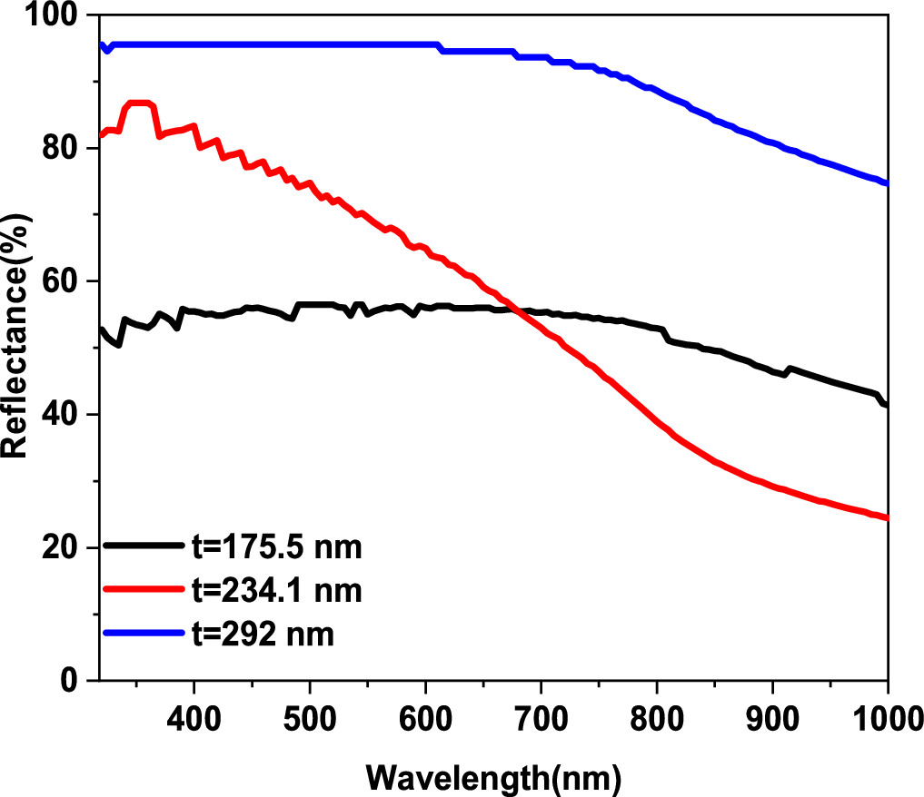
Figure 6. Reflectance spectra for CuO thin films elaborated by spray pyrolysis.
Download figure:
Standard image High-resolution image3.3.2. Optical band gap energy
The band gap energy (Eg) of copper oxide thin films was determined by Tauc's relation [28].

Eg is the optical band gap and A is a characteristic parameter independent of photon energy. Figure 7 shows (αhυ)2 = f(hυ) for the determination of the direct band gap of the CuO semiconductor by extrapolating the linear part of the graph. As illustrated, the band gap energy of film deposited by different thickness to be found 1.14 eV, 1.61 eV and 1.53 eV for t = 175.5 nm, t = 234.1 nm and t = 292 nm respectively. This results, may be explained by the morphological properties and the interband transition because of the film thickness. The suitable value of band gap energy is 1.53 eV this is not far from the absorber layer's 1.5 eV optimum for solar conversion [29] and seen at t = 292 nm.

Figure 7. Band gap energy of CuO thin films.
Download figure:
Standard image High-resolution image3.4. Electrical properties and figure of merit
The electrical characteristics of thin CuO films created via spray pyrolysis techniques were evaluated by the four-point probe. A current has been passed through the two outer probes and the voltage will have reported by the inner probes. The formula below can be used to calculate electrical square resistance Rs [23]:

The instrument measures the Rs square resistance. The calculation of electrical resistivity was performed via the formula shown below [30]:

d is the film's thickness and the following equation has been used to calculate conductivity:

The results are presented in table 3. It is clear that, film deposited by film thickness t = 292 nm has the high conductivity with low resistivity.
Table 3. Electrical characteristics of spray-pyrolyzed CuO thin films
| Solution volume (ml) | Thickness (nm) | Electrical sheet Resistance(MΩ/□) | Resistivity (Ω.cm) | Conductivity (×10−3 Ω.cm)−1 |
|---|---|---|---|---|
| 15 | 175.5 | 16.58 | 291.09 | 3.43 |
| 20 | 234.1 | 12.26 | 287 | 3.48 |
| 25 | 292 | 6.9 | 132 | 7.52 |
The figure of merit is often used as a performance indicator for conducting films. Two critical metrics used to assess the quality of transparent conducting oxides are optical transmittance and electrical conductivity [31]. The figure of merit (F) correlate these two parameters by the following formula [32]:

ρ: the electrical resistivity
T : the typical transmittance in the 600–1000 nm wavelength region.
The figures of merit were determined to be 1.9 × 10⁻³ Ω−1cm−1, 3.5419 × 10⁻³ Ω−1cm−1, and 2.4 × 10⁻³ Ω−1cm−1, respectively, for the CuO thin films of 175.5 nm, 234.1 nm, and 292 nm. These findings concur with those made by Cho et al [11]. According to the experimental results (figure 8), depositing high-quality CuO films requires a growth thickness of 234.1 nm and that maybe related to the high transmittance.

Figure 8. CuO thin films' figure of merit.
Download figure:
Standard image High-resolution image3.5. Numerical modeling of CuO absorber
The present work uses SCAPS- 1D to simulate CuO/TiO2 /FTO solar cell as shown in figure 9, which n-type window layer is of TiO2, p-type absorber layer is of CuO, FTO is used as a front contact and Au is a back contact. The aim of this work is twofold: first, to identify the optimal bandgap energy values based on experimental results, and second, to expand the thickness range of the CuO absorber layer. This will be achieved through the use of SCAPS-1D. Layer thickness of TiO2 was acquired from the literature [18]. Table 4 lists the material parameters used in the simulation were selected from earlier studies [17, 33, 34]. The back and front parameters of solar cells are listed in table 5. All the simulation experiments were obtained under 300 K of the surrounding air temperature, AM1,5 G of the solar spectrum with a light power of 1000 W m−2 . Figure 10 compares the performance of CuO/TiO2/FTO solar cell to depict the J-V characteristic. Table 6 displays the four solar cell characteristics Voc, Jsc, FF, and PCE using the values of the gap energy and the thickness of the absorbing layer that were determined from the results of the experiment. The CuO absorber layer with an energy gap value of 1.53 eV and thickness of 292 nm produces the highest efficiency of 13.38%, Voc = 0.94 V, Jsc = 17.31 cmA cm−2 and FF = 81.47%. These findings could potentially be associated with the band gap energy of the CuO absorber layer, which is 1.53 eV, a value in close proximity to the optimal 1.5 eV for solar conversion [29], this energy value would provide a good balance between optical absorption and electrical conductivity for CuO-based solar cells.
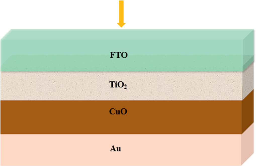
Figure 9. Schematic of the n-TiO2/p-CuO heterojunction solar cell.
Download figure:
Standard image High-resolution imageTable 4. Physical characteristics of the layers used in this simulation [17, 33, 34].
| Parameters | FTO | n-TiO2 | P-CuO |
|---|---|---|---|
| Thickness(μm) | 0.5 | 0.3 | variable |
| Band gap (eV) | 3.5 | 3.2 | Experimental values |
| Electron affinity | 4 | 4.2 | 4.07 |
| Dielectric permittivity (relative) | 9 | 10 | 18.1 |
| Conduction band (1/cm3) | 2.2 × 10¹⁸ | 2 × 10¹⁷ | 2.2 × 10¹⁹ |
| Valence band (1/cm3) | 1.8 × 10¹⁹ | 6 × 10¹⁷ | 5.5 × 10²⁰ |
| Electron mobility (cm2/Vs) | 20 | 102 | 10 × 101 |
| Hole mobility (cm2/Vs) | 10 | 25 | 10−1 |
| Shallow uniform donor density (1/cm3) | 2 × 10¹⁹ | 1017 | 0 |
| Shallow uniform acceptor density (1/cm3) | 0 | 0 | 1016 |
Table 5. Parameters of back and front contacts [34].
| Parameters | Front contact | Back contact |
|---|---|---|
| Surface recombination velocity of electrons (cm/s) | 107 | 105 |
| Surface recombination velocity of holes (cm s−1) | 105 | 107 |
| Metal work function (eV) | 4.4 | 5.1 |

Figure 10. J-V characteristic of CuO /TiO2/FTO solar cell.
Download figure:
Standard image High-resolution imageTable 6. Performance parameters of active layer.
| Eg(eV) | Voc(V) | Jsc (cmA/cm2) | FF(%) | PCE(%) | |
|---|---|---|---|---|---|
| t = 175.5 nm | 1.14 | 0.56 | 24.06 | 75.39 | 10.31 |
| t = 234.1 nm | 1.61 | 1.02 | 14.21 | 81.53 | 11.84 |
| t = 292 nm | 1.53 | 0.94 | 17.31 | 81.47 | 13.38 |
3.5.1. Impact of absorber layer thickness
Layer absorber thickness has a direct impact on photovoltaic solar cell performance. Figure 11 provides a visual representation of the investigation into the cell's performance. This examination involved the variation of the CuO absorber layer's thickness, ranging from 0.1 μm to 1 μm, with the band gap energy set at 1.53 eV, while holding the remaining parameters constant.

Figure 11. CuO thickness effect.
Download figure:
Standard image High-resolution imageFigure 11 demonstrates that Voc, Jsc, FF and PCE rise with the thickness of the absorbent layer, which can be explained by the significant absorption of long-wavelength photons that boost photogeneration [35, 36]. However, the highest value is observed at 1 μm.
Figure 12 displays the quantum efficiency (QE) as a function of wavelength, where it is defined as the ratio of carriers collected by the solar cell to incident photons with a particular energy.

Figure 12. Effects of CuO p-type absorber layer thickness on quantum efficiency.
Download figure:
Standard image High-resolution imageHow well a material transforms photons into an electrical current or charge is known as its quantum efficiency. A CuO absorber layer's quantum efficiency may peak at a wavelength around 370 nm, which could mean the material excels in converting photons of that particular wavelength into an electrical current or charge. As it can have seen the cell's reaction to incident sunlight becomes more favorable when the absorber layer thickness increases. Furthermore, the most favorable response is evident within the wavelength range of 400–800 nm, with absorption tapering off beyond 870 nm. The optimal value for absorber layer thickness is 1 μm.
3.5.2. Influence of temperature on solar cell performance
Figure 13 shows the temperature effect on n-TiO2/p-CuO solar cell, Voc and Jsc are decreased when the temperature value increases. Moreover, the fill factor and efficiency indicate high values at low temperature. The high values of FF and PCE found to be 85.05% and 19.24% corresponding at 295 K. This drop of efficiency as temperature rises is due to an increase in the rate of electron and hole recombination [15]. According to this analysis, the proposed cell is more suitable for high efficiency in low-temperature parts of the world.

Figure 13. The temperature effect on theTiO2/CuO solar cell.
Download figure:
Standard image High-resolution image
4. Conclusion
In order to study the impact of the film thickness, spray pyrolysis techniques have been used to elaborate CuO thin films. According to the x-ray diffraction characterisation, CuO thin films exhibit a monoclinic structure, and as thickness increases, the peak intensities rise. Besides that, SEM images show a dense and uniform surface for films. Additionally, optical study shows that CuO thin films work better as they get thicker, show strong absorbance in the wavelength range of 300–600 nm, and have increasing band gap values. Based on the electrical data, the preferred combination is a thickness of 292 nm with a band gap energy of 1.53 eV, showcasing excellent conductivity and low resistivity. These outcomes find reinforcement in the simulation's performance results. Using the data from the experimental study, SCAPS-1D was employed for the numerical simulation of the CuO solar cell. The sample with t = 292 nm and Eg = 1.53 eV scored the best efficiency with 13.8%. CuO-based solar cells have shown that increasing the thickness of the absorbing layer has a favourable effect. Additionally, the findings of the simulation show that a rise in operating temperature has a detrimental impact on the performance of solar cells.
The authors acknowledge Prof. Burgelman's and a group of the University of Ghent to developed SCAPS-1D program used in this work.