
Abstract
Optical imaging systems have greatly extended human visual capabilities, enabling the observation and understanding of diverse phenomena. Imaging technologies span a broad spectrum of wavelengths from x-ray to radio frequencies and impact research activities and our daily lives. Traditional glass lenses are fabricated through a series of complex processes, while polymers offer versatility and ease of production. However, modern applications often require complex lens assemblies, driving the need for miniaturization and advanced designs with micro- and nanoscale features to surpass the capabilities of traditional fabrication methods. Three-dimensional (3D) printing, or additive manufacturing, presents a solution to these challenges with benefits of rapid prototyping, customized geometries, and efficient production, particularly suited for miniaturized optical imaging devices. Various 3D printing methods have demonstrated advantages over traditional counterparts, yet challenges remain in achieving nanoscale resolutions. Two-photon polymerization lithography (TPL), a nanoscale 3D printing technique, enables the fabrication of intricate structures beyond the optical diffraction limit via the nonlinear process of two-photon absorption within liquid resin. It offers unprecedented abilities, e.g. alignment-free fabrication, micro- and nanoscale capabilities, and rapid prototyping of almost arbitrary complex 3D nanostructures. In this review, we emphasize the importance of the criteria for optical performance evaluation of imaging devices, discuss material properties relevant to TPL, fabrication techniques, and highlight the application of TPL in optical imaging. As the first panoramic review on this topic, it will equip researchers with foundational knowledge and recent advancements of TPL for imaging optics, promoting a deeper understanding of the field. By leveraging on its high-resolution capability, extensive material range, and true 3D processing, alongside advances in materials, fabrication, and design, we envisage disruptive solutions to current challenges and a promising incorporation of TPL in future optical imaging applications.
Highlights
Provide a comprehensive overview of two-photon polymerization lithography (TPL)-based imaging applications.
Introduce the fundamental imaging theories, key materials properties, and fabrication technologies.
Classify and summarize the various imaging applications of TPL.
Envisage the future trends of TPL for imaging optics and offer insights on the potential solutions to current challenges.
Export citation and abstract BibTeX RIS

Original content from this work may be used under the terms of the Creative Commons Attribution 4.0 license. Any further distribution of this work must maintain attribution to the author(s) and the title of the work, journal citation and DOI.
1. Introduction
Optical imaging is the process of creating an accurate representation of objects through optical devices, akin to how humans perceive their surroundings and objects with their eyes [1]. This traditional yet continually evolving field has been under investigation for millennia, progressing alongside the development of theories, materials, designs, technologies, and diverse applications [2]. Optical imaging systems extend beyond the visual capabilities of the human eye, broadening the scope of human observation and comprehension with large-aperture telescopes for the exploration of the universe, and microscopes for the microscopic realm, fostering advances in biology, chemistry, medicine, and other related disciplines. Furthermore, optical imaging has transcended the visible light spectrum, encompassing x-ray, ultraviolet (UV), infrared, terahertz, microwaves, and radio frequencies [3]. The continuous enhancement of optical imaging technologies regarding spatial and temporal resolution, spectral sensitivity, detection capabilities, and multidimensional imaging has facilitated their widespread integration into consumer electronics like smartphones, drones, and virtual reality glasses, greatly enhancing daily life.
Traditional methods for fabricating glass-based lenses involve multiple intricate steps such as glass blank molding, casting, annealing, diamond turning and shaping, and rough and fine abrasive grinding. Additionally, achieving composite homogeneity and precise phase modulation necessitates complex measurements and melt pedigree calculations. In contrast, as the representative flexible materials, polymers have gained popularity over recent decades due to their low cost, light weight, fabrication flexibility, and high transparency, employing simpler techniques like injection molding and UV curing. They can also serve as stable host matrices for molecules, nanoparticles, and nanocrystals for various optical applications. Generally, a lens with a surface roughness below one-tenth of a wavelength suffices in most applications. However, in contemporary imaging applications, a lens alone often fails to meet the diverse requirements across various scenarios, where the lens sets are required to improve imaging quality, a strategy commonly employed in telescopes, microscopes, and mobile phones. This necessarily introduces time-consuming assembly and sophisticated alignment of multiple lenses along with motors, filters, image sensors, and other optical modules. Furthermore, modern optical imaging devices favor the minimization, portability, and integration, which is beyond the conventional bulk lens. In this spirit, recent advancements in principles of lens design span from refractive optics to diffractive optics and nanophotonics, aiming to achieve unprecedented imaging capabilities with thin, lightweight optical devices to supplement the traditional ones [4–7], as for the latter, it is particularly hard to obtain micro- and nanoscale structures, thereby limiting their potential applications.
Three-dimensional (3D) printing, also known as additive manufacturing (AM), offers a promising solution to the aforementioned challenges associated with traditional fabrication methods [8]. It eliminates alignment requirements for fabricating various numbers of lenses and enables the production of optical devices with small-scale features. Additionally, 3D printing offers numerous advantages, including rapid prototyping, customized geometries, minimal waste generation, and short manufacturing time. The intrinsic properties of polymers used in 3D printing, such as high transparency, homogeneity, and low surface roughness, position them as ideal candidates for miniaturized optical imaging devices, especially for the visible band applications due to the absence of absorption bands. Various 3D printing methods, including extrusion-based fused filament fabrication, direct ink writing, and fused deposition modeling, as well as optical-based techniques like digital light processing, laser stereolithography, continuous liquid interface production, polymer jetting, computed axial lithography [9], and xolography [10], have been employed to fabricate micro- to centimeter-scale optical objects with exceptional quality. In general, critical parameters considered with AM technologies in imaging device manufacturing encompass commercial printer, build volume, feature size, printing speed, optical material capabilities, post-processing treatments, homogeneous optical properties, preservation of pristine material properties, uniform surface interfaces, etc [11]. Despite the advantages of these 3D printing methods over traditional fabrication techniques, they still face limitations in achieving spatial resolutions at the nanoscale and delivering low surface roughness for complex 3D devices, restraining themselves to the macroscale components [12].
Among the most promising nanoscale 3D printing techniques, two-photon polymerization lithography (TPL) empowers the fabrication of arbitrary structures with feature sizes surpassing the optical diffraction limit [13–15]. The principle underlying TPL involves focusing a femtosecond pulsed laser through a high-numerical-aperture (NA) objective lens, creating a focal spot within an uncured liquid photoresist. The photoresist only polymerizes upon the induction of two-photon absorption, the probability of which is proportionate to the square of the light intensity. This nonlinear process is several orders weaker than single-photon absorption, restricting photopolymerization to the central volume of the focal spot, where the intensity surpasses the threshold, forming a voxel. Subsequently, the designed 3D structure can be printed by segmenting it into layers, with each layer divided into hatching lines. The laser beam then scans along these paths in the photoresist with optimized printing speed and laser power to shape the model with voxels [16–19].
TPL offers multiple advantages, including alignment-free single-step fabrication, the ability to realize micro- and nanoscale features, and rapid production of high-quality structures [20]. Its extensive application spectrum spans optical and nanophotonic domains [21–24], encompassing refractive optics, diffractive optical elements, photonic circuits, topological photonic crystals, quantum optics, and optical robots. Notably, TPL serves as a powerful tool for fabricating miniaturized optical imaging systems, as previously explained. In this comprehensive review, we first revisit key parameters for assessing imaging performance, advocating for the comprehensive optical characterization of 3D-printed imaging devices. Subsequently, we introduce critical material properties for TPL, such as conversion degree, transmission, dispersion, thermal stability, and mechanical stability, which exert a substantial influence on imaging quality. We also provide a meticulous summary of the techniques employed for fabricating imaging systems through TPL on various substrates, including glass, fiber, chips, and image sensors (complementary metal–oxide–semiconductor, CMOS, and charge-coupled device, CCD). Following this, we report on the development of TPL for optical imaging applications, covering various categories such as refractive lenses, diffractive lenses, metalenses, gradient index lenses, lens arrays, compound eyes (CEs), dynamic lenses, endoscopic lenses, diffractive optical neural networks, computing imaging, and other optical imaging systems (figure 1). It is expected to furnish researchers with a comprehensive review that allows them to grasp the foundational knowledge and recent advancements, fostering a thorough understanding of this field. Finally, leveraging TPL's high-resolution processing abilities, extensive material processing range, and genuine 3D processing capabilities, in conjunction with recent progress in new materials [25–28], fabrication technologies [29], and design methodologies [30], we discuss potential solutions to current challenges and prognosticate the prospects of TPL in the realm of imaging optics. Although TPL offers numerous advantages over traditional fabrication methods, its application in industrial production is still in its infancy and confronted with various limitations like suitable materials and direct fabrication speed. The sluggishness contributes to elevated costs, constituting a primary constraint for this technique. Despite this limitation, TPL proves well-suited for rapid prototyping and mold creation for uniquely shaped imaging elements, thus facilitating the production of devices with specialized functions. We envision that through the fusion of fundamental principles governing optical imaging, materials, innovative designs, and novel fabrication techniques, TPL will persist in revolutionizing this field, furthering our comprehension of the world through imaging.

Figure 1. Schematic of two-photon polymerization lithography for imaging optics, including categories of evaluation criteria, materials, fabrication technologies, and various applications. Reproduced from [32]. CC BY 4.0. Reproduced from [31]. CC BY 4.0.
Download figure:
Standard image High-resolution image2. Imaging evaluation
The evaluation criterion of an optical imaging system is vital to quantify the quality of the system and to compare its performance with others. Though various categories of imaging elements and devices have been fabricated via TPL, a systematic introduction of evaluation methods is still lacking in the literature, and some key parameters are not mentioned. In general, the evaluation standards built for traditional imaging systems can still be applied to micro and nanoscale imaging systems. As shown in figure 2, here we aim to address the evaluation criterion by starting with an overview of the important designing parameters of the imaging system, followed by an introduction of the basic definitions and a summary of aberration theories. The minimization of aberration is the optimization objective in the design process of the imaging system, which is also an image quality evaluation index. Finally, we introduce the fundamental imaging quality evaluation methods, which can reflect the design parameters and aberrations of the imaging system, hence in turn could be employed to optimize the design and fabrication parameters.
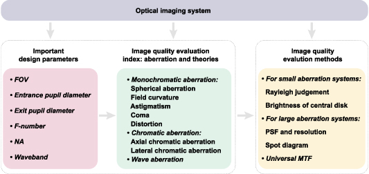
Figure 2. Designing parameters and imaging quality evaluation methods for optical systems.
Download figure:
Standard image High-resolution image2.1. Important design parameters
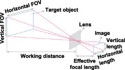
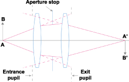
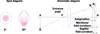
The establishment of basic design parameters is critical in the design process of an optical system, as they are tailored to specific requirements and application scenarios. In this part, the definition and the effect of the important parameters of the optical system are summarized, as demonstrated in table 1.
Table 1. Summary of important design parameters.
| Term | Definition | Schematic diagram |
|---|---|---|
| Field of view | FOV = 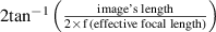
|
|
| Entrance pupil and exit pupil | Entrance pupil: the effective aperture that limits the incident beamExit pupil: the public exit after the imaging light of each point on the object surface passing through the entire optical system |
|
| F-number |
F/# =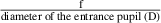
| — |
| Numerical aperture | NA = n•sin(θ)n: environment refractive index θ: angle between the light rays passing through the edge of the aperture and the optical axis | — |
| Waveband | The wavelength bandwidth range in which the optical system operates | — |
2.2. Imaging quality evaluation index: aberration theories
The quality of any image will be reduced due to the existence of geometric aberration and diffraction. Therefore, when an object point passes through the optical system, what it presents on the image plane is no longer an ideal point but a circle of confusion. Hence, analyzing and optimizing aberrations to minimize their effects is crucial for system design. Aberration can be categorized into two main categories: geometric aberration and wave aberration. Among them, geometric aberration can be further categorized into monochromatic aberration and chromatic aberration, the specific classification of monochromatic aberration is shown in table 2 with their relations to lens geometric parameters in table 3, and the specific classification of chromatic aberration is illustrated in table 4.
Table 2. The definition and the corresponding phenomenon of monochromatic aberrations.
| Term | Definition | Phenomenon |
|---|---|---|
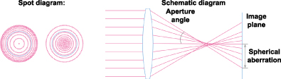
| Spherical aberration | Light rays near the center of the lens and away from the center of the lens converge at different points in the optical axis |
|
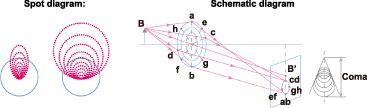
| Coma | The edge rays and the central rays of a beam emitted from an off-axis object point will form different intersection points with the ideal image plane |
|
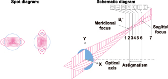
| Astigmatism | The difference in the focusing ability between a thin beam on the meridian plane and a thin beam on the sagittal plane |
|
| Field curvature | When different points on the object surface pass through the same optical system, different image points will be formed which forms a curved plane |
|
| Distortion | The difference in magnification between the periphery and the center of the object is different |

|
Table 3. Summary of third-order monochromatic aberration dependence on aperture and FOV.
| Aberration | Aperture dependence | FOV dependence |
|---|---|---|
| Spherical | Cubic | — |
| Coma | Quadratic | Linear |
| Astigmatism | Linear | Quadratic |
| Field curvature | Linear | Quadratic |
| Distortion | — | Cubic |
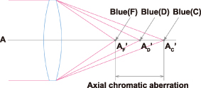
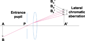
Table 4. The definition and the corresponding phenomenon of chromatic aberrations.
| Term | Definition | Schematic diagram |
|---|---|---|
| Axial chromatic aberration | The image points of different colors of light are not in the same position on the optical axis |
|
| Lateral chromatic aberration | The main ray of different lights emitted by the same off-axis object point will form different intersection points with the ideal image plane |
|
2.2.1. Monochromatic aberration.
As for the above geometric aberrations, Fischer et al made a summary as shown in table 3, which reflected the degree of influence of field of view (FOV) and entrance pupil diameter on the above aberrations [33].
2.2.2. Chromatic aberration.
See definitions and the corresponding phenomenon of chromatic aberrations in table 4.
2.2.3. Wave aberration.
When a spherical wave passes through the optical system, a new spherical wave will be formed ideally, which, in fact, is often deformed to some extent and not an ideal spherical wave, as shown in figure 3.
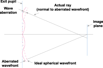
Figure 3. Illustration of wave aberration.
Download figure:
Standard image High-resolution image2.3. Imaging quality evaluation methods
In the process of image quality evaluation, if diffraction effects are not considered, the image quality is mainly affected by system aberrations, in this case, the image quality can be evaluated based on the above aberration theories. When diffraction and geometrical optical aberration exist simultaneously, some more systematic evaluation methods have been introduced, while the choice of evaluation method depends on the aberration characteristics of the designed optical systems. For small aberration systems, Rayleigh criterion and brightness of central disk methods are commonly used. As for the large aberration systems, the image quality is generally evaluated by point spread function (PSF), resolution, spot diagram, and star test method. Modulation transfer function (MTF) is a universal evaluation method applicable to both large aberration systems and small aberration systems. Since TPL is applicable for the fabrication of ray tracing-based lens, diffractive lens, and even metalens, the evaluation methods introduced here could be employed to compare their performances in a more efficient and reliable way.
2.3.1. For small aberration systems
2.3.1.1. Rayleigh criterion.
Rayleigh criterion is a criterion proposed by Lord Rayleigh during the observation of spectrometer imaging quality, which dictates that the optical system's performance remains largely unaffected if the maximum optical path difference caused by aberrations does not exceed one-quarter of the wavelength.
2.3.1.2. Brightness of central disk.
Strehl proposed the ratio of the maximum brightness in the diffraction pattern with aberration to the maximum brightness without aberration to represent the image quality of an optical system. This ratio is called the center point brightness, denoted by S.D. Strehl pointed out that the system is considered workable when the center point brightness S.D. is greater than or equal to 0.8.
2.3.2. For large aberration systems
2.3.2.1. PSF and resolution.
For an optical system, the light field distribution on image plane corresponding to a point on the object plane passing through the system is called PSF. The concept of PSF also can be used to determine the resolution of the optical system.
The resolution of an optical system refers to the minimum distance between two closely spaced object points that can be resolved by the optical system. This index reflects the ability of the optical system to resolve the fine structure of the object. Rayleigh pointed out that 'two images are just resolvable when the center of the diffraction pattern of one is directly over the first minimum of the diffraction pattern of the other,' as shown in figure 4(a). The distance between the two peak points in the figure is:

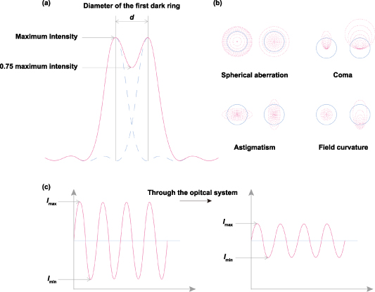
Figure 4. Illustration of the evaluation methods. (a) Resolution. (b) Spot diagrams. (c) MTF.
Download figure:
Standard image High-resolution imageThis formula is the basic formula to calculate the theoretical resolution of an optical system. This formula is also the formula for calculating Airy disk radius (diffraction limit). Since any optical system is affected by geometric aberration, the actual spot radius is difficult to exceed the diffraction limit.
2.3.2.2. Spot diagram and star test.
After many light rays from one point pass through the optical system, due to the existence of aberration, the intersection point between them and the image plane is no longer a point but forms a diffuse pattern, which is called a spot diagram. The imaging quality of the system can be measured according to the density of the points and the shape of the distribution pattern. Since the spot diagram ignores the diffraction effect, it only reflects the degree of aberration of the system. Here, the distribution of the spot diagram under different aberrations is listed, as shown in figure 4(b).
The principle of the star test method is similar to that of spot diagram. Since the distribution of any object can be regarded as the collection of countless independent luminous points with different intensities, the image of any object is the collection of countless star point images, so the imaging quality of the system can be judged by the distribution function of light intensity of the star image. Unlike the spot diagram, which is an evaluation method used in the design process, the star test is adopted after the optical system is manufactured.
2.3.2.3. Universal method
2.3.2.3.1. MTF.
The above image quality evaluation methods all have certain limitations in application, and MTF is related to both geometric aberration and diffraction effects of optical systems, so it is the most universal and comprehensive evaluation method. The MTF can be expressed as the ratio of the contrast of the image plane to the contrast of the object plane, and the contrast is represented by (Imax− Imin)/(Imax + Imin), as shown in figure 4(c). MTF can reflect the transfer ability of different frequency components. High-frequency transfer function reflects the ability of transferring details of the object, medium-frequency transfer function reflects the ability of transferring layers of the object, and low-frequency transfer function reflects the ability of transferring the contour of the object. The imaging quality of the system can be judged by the trend change of the MTF curve and the area enclosed by the curve and the coordinate axis.
Though the evaluation standards were set, it is critical to figure out how the TPL makes the imaging optics better meet these evaluation critics. Ensuring high-quality standards in the 3D printed imaging elements relies on key steps encompassing design, fabrication, and characterization. In the initial design phase, the material properties and geometries are predetermined, facilitating the quantification of these evaluation criteria through numerical simulations. During fabrication, the primary objective is to produce structures that closely mimic the design, necessitating high-resolution printing methods to minimize defects. However, achieving sharp edges and corners proves challenging due to the intrinsic shape of the voxel, the proximity effect, and the imperfect degree of polymer conversion, leading to slight shrinkage in post-processing. A judicious compromise is essential, and error robustness analysis is imperative to accommodate these factors. Additionally, optical properties may deviate from the design due to local refractive index (RI) changes induced by fluctuations in laser power, overlapped printing paths, and reflections at the substrate/resin interface. Furthermore, the evaluation of fabricated devices should occur under standard conditions, such as collimated illumination with white light, and precise power measurements. Through meticulous geometrical and optical characterizations, the acquired data can be iteratively incorporated into the design process, optimizing imaging performance by adjusting fabrication parameters. Additionally, inverse design methodologies or artificial intelligence (AI), such as deep learning, can be harnessed to identify optimal designs, accounting for real fabrication limitations to meet specific imaging standards.
3. Materials and fabrication technologies
3.1. Materials properties
The intrinsic optical, mechanical, and thermal properties of photoresists applied for imaging device fabrication are vital for the final performance. Commonly used materials include organic photoresists, such as acrylate, with Nanoscribe GmbH's IP series standing out as a successful commercial option, and hydrogels, which are more suitable for soft and dynamic optical elements due to their low mechanical properties. Epoxy, exemplified by the cost-effective and highly transmissive resin SU-8, is another noteworthy type with tunable properties and nanoscale fabrication capabilities. Hybrid organic–inorganic materials, like silicate resin ORMOCER® and silicon–zirconium hybrid SZ2080™, also exhibit promising fabrication capabilities. Compared to the inorganic counterparts, though 3D printed lenses from solidified polymers boast favorable properties for imaging optics, stability analysis is imperative for varied environments, considering potential variations in optical properties under different humidities, temperatures, and pH values of organic polymers. Available RI range, dispersion relation, and laser-induced damage threshold of polymers should also be considered for specific applications. In addition, the material properties of the fabricated optical devices are also dependent on the printing parameters during the TPL process, such as laser power and write speed. Properties like degree of conversion (DC), RI, mechanical and thermal stability, dispersion, and reflectance will be changed hereafter and may degrade the imaging quality.
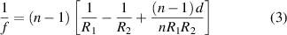
The DC value of the polymer in the TPL process can be determined by Raman micro-spectroscopy, differential scanning calorimetry, coherent anti-Stokes Raman scattering, and Fourier transform infrared spectroscopy [34, 35]. During the exposure process, the C=C bonds in the resin transfer to C–C bonds (figure 5(a)), thus the DC can be determined by measuring this chemical structure change. The DC is positively correlated to the laser power and negatively correlated to the write speed (figure 5(b)). Generally, the maximum DC is below 50% for two reasons: (1) during polymerization, the resin is polymerized and becomes solid, preventing the diffusion of free radicals and further polymerization is terminated; (2) further increasing the laser power or lowering the write speed will boil the resin due to the local thermal energy accumulation. The polymerization threshold, defining the minimum laser power for stable structure fabrication, and the burning threshold, indicating the laser power at which stable structures become unattainable due to overheating or over-polymerization, together form the fabrication window. This window represents the range between the polymerization and burning thresholds within which structures with default dimensional accuracy can be created and acceptable DC can be achieved. Overheating leads to localized issues, resulting in evaporation and the formation of disruptive large bubbles rather than an increased DC value. The extent of bubbling is influenced by the heat diffusion coefficient, with overheating manifesting in three modes of local heating, regional heating, and global heating. During the fabrication, overheating can be mitigated by adjusting laser exposure power, increasing hatching or slicing distances, or improving laser scanning speed. Iterative testing of structural geometry and qualities is crucial to achieving the required structure with suitable DC. The mechanical properties of the printed structure are closely related to DC. As the DC increases, both the reduced Young's modulus and the hardness of the structure increase (figure 5(c)). The increase of Young's modulus as the increase of laser power was also observed in both tensile and compression tests [36, 37].
Figure 5. Material properties in TPL for imaging optics. (a)–(c) Influence of degree of conversion. (a) Raman spectra of polymerized and non-polymerized IP-L 780. (b) Dependence of degree of conversion of the polymer on laser power and write speed. (c) Reduced Young's modulus and hardness of TPL printed structures as the functions of the DCs. Inset: as printed cubic structure, scale bars: 10 µm. (a)–(c) Reprinted with permission from [34] © The Optical Society. (d)–(g) Influence of the refractive index. (d) Dependence of the real part of the refractive index (n) on the laser power in one photon (left) and two photon process (right). (e) Dispersion of n of IP-dip resin fabricated layers for both one photon (green) and two photon (red) processes. (d), (e) Reprinted with permission from [38] © The Optical Society. (f) Measured n of a TPL printed gradient-index micro-optics along x and y axes. [40] John Wiley & Sons. © 2015 by WILEY-VCH Verlag GmbH & Co. KGaA, Weinheim. (g) Scanning electron microscope images (SEM) of TPL printed structures with RI of 1.491 and 1.5215, respectively. Scale bars: 1 µm. Reproduced from [41] with permission from the Royal Society of Chemistry. (h)–(j) Shrinkage of the TPL printed materials. (h) TPL printed three-dimensional photonic crystal structures with ultra-low shrinkage resin. Reprinted with permission from [42]. Copyright (2008) American Chemical Society. (i) SEM images of acrylate-based (left) and nano particles-based (right) resins printed structures after pyrolysis under 1000 °C in air. [43] John Wiley & Sons. © 2021 The Authors. Small published by Wiley-VCH GmbH. (j) SEM images of a microscopic mushroom-shaped pillar after conventional (upper) and UV post curing (lower) developments. Reprinted from [44], © 2018 The Authors. Published by Elsevier B.V. (k)–(n) TPL of opaque materials. (k) Transmission as a function of printed layer thickness for a highly absorptive resin. (l) A TPL printed hybrid singlet lens with the prototype IP-Black aperture. (m) and (n) The imaging performance of the singlet lens without and with the Prototype IP-Black aperture. (k)–(n) [49] John Wiley & Sons. © 2022 The Authors. Advanced Functional Materials published by Wiley-VCH GmbH. (o)–(q) Atomic layer deposition (ALD) of TPL printed structures. (o) Illustration of transmission through an uncoated and AR coated lens. (p) SEM image of a cleaving face of an ALD coated silicon reference wafer. (q) Reflectivity of coated and uncoated 3D printed flat structure shown in the inset. The coating is on both sides of the sample. (o)–(q) . . Reprinted with permission from [51] © The Optical Society.
Download figure:
Standard image High-resolution imageRI is another key optical parameter that will be affected by the printing process. The RI increases as the laser power increases (figure 5(d) right), while the RI of TPL fabricated samples is slightly lower than those from one photon process (figure 5(d) left) [38]. There is dispersion of RI in both one photon process and TPL fabricated polymers (figure 5(e)). Generally, it can be fitted by the Sellmeier dispersion function  , where n is the RI, λ is the wavelength, and parameters A and B can be determined by ellipsometry experimentally [39]. By tuning the laser power, the RI of the structure can vary locally inside one single structure. By employing a 'zig-zag' approach, with exposure dosage increasing toward the center and decreasing toward the opposite edge along the horizontal direction (x-axis), lens with RI modulation in one direction can be printed. Measurement confirms continuous variation of RI in the x-direction inside a single lens structure (figure 5(f)) [40], thus, gradient lens fabrication is possible by modulating the local RI. In addition, the RI of the unpolymerized resin will also affect the precision of the printed structure since the resin RI should match the RI of the immersion medium for which the objective lens was initially designed. PSF could be used to simulate the 3D diffraction pattern of light transmitted through resin and provide a quantified evaluation standard. For example, to match the RI of common immersion oils in the dip-in TPL configuration, an RI of 1.52 is designed. Mismatch of the RI results in elongation of voxel with aspect ratios as big as 6 and also leads to distortion of the printed structure (figure 5(g)) [41].
The mechanical stability of the TPL materials is another important factor to influence the optical performance as it is very sensitive to the geometric structure and surface morphology. Several materials and material processing methods have been developed to enhance mechanical performance. For most resins used in TPL, there is a certain degree of shrinkage when the liquid resin polymerizes into solid state. Alternatively, organic–inorganic hybrid gels can be used to reduce the shrinkage. In this process, the organic groups attached to the inorganic parts are polymerized by TPL, which results in linking together the pendant methacrylate groups of the resin without the release of any molecules, and no obvious shrinkage is observed (figure 5(h)) [42]. Besides, to reduce the shrinkage of sintering-based TPL, a large amount of inorganic nano particles can be added to the organic resin [43]. The organic acrylate-based structure shows a linear shrinkage of 53%, while the nano particles-based structure shows only 19% of linear shrinkage when sintering at 1000 °C (figure 5(i)). The Young's modulus and the hardness of the TPL structure can be enhanced by increasing the DC, as discussed above. However, increasing the DC during printing requires a higher laser power, which may reduce the resolution of the final structure. To avoid sacrificing the resolution, the DC can be tuned by post processing, such as UV exposure. A comparison study shows that the final structure is distorted due to the low mechanical strength, while the UV exposed structure is more stable (figure 5(j)) [44].
Commonly used polymetric structures suffer from thermal degradation and are not suitable for high temperature environment applications such as laser optics. Adding inorganic substances into the resin and sintering after printing can produce thermal resistance devices for optics, for example, titanium [45], silicon, silica [46, 47], nickel [48], and zirconia [43], can be added to the polymer matrix. Sintering of these hybrid materials in air can remove the organic part and produce corresponding oxides to improve thermal stability. Most of the above-mentioned materials are highly transparent with low absorption in the visible and near infrared (NIR) range. For some optical applications such as apertures, opaque materials can help to increase the imaging contrast. For this purpose, some black materials suitable for TPL are developed. One example is the commercial prototype photoresist IP-Black (Nanoscribe GmbH & Co. KG). By tuning the thickness, the transmission can be tuned to obtain different gray levels (figure 5(k)) [49]. Optical devices such as apertures and absorptive tubes can be directly printed (figure 5(l)). Imaging results show that the transparent aperture exhibits a weak image contrast (figure 5(m)), while the black aperture can improve the contrast significantly (figure 5(n)). The black materials can also be deposited onto the structure after TPL printing by other techniques such as inkjet for large area applications [50]. Another way to add different materials onto the TPL printed structures to enhance the optical performance is atomic layer deposition (ALD). For example, by ALD, anti-reflective (AR) coatings consisting of four alternating layers of titania (TiO2) and silica (SiO2) can be added onto a TPL printed lens (figures 5(o) and (p)), or they can be used on waveguides to tune the optical properties or to protect the polymer structures from harsh environments. Reflectivity measurements show that the ALD coated structure has a much lower reflectivity than the uncoated structure (figure 5(q)).
3.2. Fabrication
TPL technology offers great flexibility in terms of structures and materials. High-resolution complex 3D structures can be fabricated using a range of materials like polymers [52], ceramics [53], and even metals [54]. TPL is a three-step photochemical process: initiation, propagation, and termination [55]. The process is initiated by a femtosecond laser beam (figure 6(a)). Upon initiation, the photoinitiators in the resin absorb two photons simultaneously and reach the excited state (figure 6(b)). This step also involves the generation of radicals from the decomposition of the photoinitiators, and they combine with monomers in the propagation step to generate monomer radicals. In the final step, the monomer radicals combine to terminate the photopolymerization process. TPL is a nonlinear process which uses a degenerate two-photon absorption process, where both of the absorbed photons are of the same frequency [56]. The polymerization process begins only when the exposure dose is beyond a certain threshold for a constant laser power or vice versa. Such a threshold limit and optical nonlinearity make it possible to achieve high resolutions, which are impossible to achieve with other AM techniques [57]. Computer generated 3D model of the structure to be fabricated is first sliced in z-direction to layers of desired thickness, then each slice is divided to define laser focus points that form the trajectory for beam movement in the x- and y-directions. During the fabrication process, laser beam is moved along this trajectory in the liquid resin volume, exposing the resin only at the focal point to build the desired structure. Unexposed resin is then removed using specific solvents during development phase to get the final structure. The optical performance of obtained elements is affected by various factors, e.g. the internal uniformity, surface roughness, and structural deformation, for which the related fabrication technologies have been briefly introduced above and detailed summarized in [13]. Here, we mainly focus on the fabrication methods on different substrates and facets of fibers, which will greatly expand the application scenarios of TPL related imaging optics.
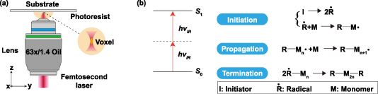
Figure 6. Schematic of TPL fabrication and the three-step photochemical process at the focal spot. (a) A femtosecond laser beam is focused via a high NA objective lens into the photoresist to induce polymerization process at the focal spot. (b) Two-photon absorption process and the three-step photochemical process with initiator, radical and monomer.
Download figure:
Standard image High-resolution image3.2.1. Fabrication on flat substrates.
The requirement for higher functionality integration and miniaturization in silicon photonic circuits and complex optical systems was mainly limited by the restrictions posed by the conventional fabrication methods on the achievable geometries. With the development of TPL and compatible transparent resins, optical components with sub-100 nm resolution and any arbitrary geometries could be realized, which is conducive to significant developments in several fields of optics. Moreover, the ability of the process to fabricate on different substrate systems like glass, silicon and even optical fibers makes it a promising technique to manufacture integrated components [58, 59]. For example, free-form optical elements can be found as a major component in on-chip as well as fiber-based optics. With conventional technologies, it is difficult to fabricate such optical elements on a CMOS chip or on the facet of a single mode fiber (SMF). Direct laser fabrication on absorptive or reflective surfaces is challenging as there is a risk of ablation at the polymerization threshold. Works have demonstrated 3D printing on substrates with different reflectivity using femtosecond laser writing [60, 61]. In an initial work, the printability on substrates with different reflectivity (glass, silicon and black silicon) was demonstrated with a woodpile structure fabrication. The substrate with the lowest reflectivity (b-Si) is seen to be giving high quality structures for a wide range of irradiance. It was shown that highly reflective surfaces resulted in damaged prints as can be seen in figure 7(a) [62]. Phenomena like reflections, light field enhancement and heating at the substrate–resin interface enhance the polymerization and thus trigger micro explosions even at the base levels of the structures. Such explosions result in degraded optical performance, poor structural stability and detachment on reflective/metal substrates. Hence, for such substrates, stringent dose control is required for the interface layers. Later advancements in process techniques and precise control over the exposure doses have enabled TPL to fabricate conventional and non-conventional optical elements directly on reflective surfaces like LED chips with precise control over the structure (figure 7(b)) [63]. Another example of an advanced optical system is a multi-focal lens [64], which is fabricated as a combination of multi-focal diffractive zone plate and an aspheric lens. A tri-focal lens and the output measurement with three foci are shown in figure 7(c). As this compound lens has specific surface profiles on both faces, fabrication is a combination of two processes. The diffractive binary zone plate is fabricated using TPL on a circular glass substrate. The bottom refractive lens is fabricated by casting resin into a negative mold of desired profile. Then, the glass substrate with the diffractive zone plate is precisely positioned on the resin-filled mold surface and the resin is cured to give the final compound lens. Such lenses can be of particular interest as intraocular lenses for cataract patients as they may provide sharper vision at different distances. Availability of biocompatible materials for TPL also makes it feasible to use this process for such applications. Integration of imaging optics on CMOS platform is of growing interest due to the wide range of lens profile designs that can be realized using TPL. Wafer level integration for foveated imaging was demonstrated with miniaturized cameras where an MLA fabricated via photolithography technique forms sub-images which are stitched to form the final image [65]. A more effective imaging system was demonstrated using aberration corrected air-spaced doublet objective array fabricated using TPL directly on a CMOS image sensor [66]. A more straightforward and dose tolerant method was used in the demonstration of bionic micro CE camera with a 90° FOV capable of imaging micro-organisms [67]. In this work, the CE lens was first printed on a cover-glass substrate. This leverages on the standard printing conditions and relaxes the need for precise dose control to prevent structural damage, which is a possibility when directly fabricating on CMOS. The cover glass with the CE lens is then cut to smaller size to fit the CMOS chip using a UV curable adhesive (figure 7(d)). In addition, the optical elements can also be fabricated on the surface of light sources such as vertical-cavity surface-emitting lasers to perform wavefront modulation directly [68]. Such TPL fabricated systems are superior to imaging systems realized using other fabrication techniques as they enable miniaturization, give precise control on the structure profile and deliver high imaging quality. All of these works have clearly defined the advantages of TPL over conventional fabrication techniques in terms of process complexity and, more importantly, the freedom of achievable geometries for imaging optics fabrication on different substrates.

Figure 7. Fabrication on different substrates with TPL. (a) SEM images of woodpile structures printed on substrates with different reflectivities. Red highlighted boxes show high quality 3D structures. Reprinted with permission from [62] © The Optical Society. (b) 3D printed compound parabolic concentrator (CPC) on a chip in a TO-18 metal packaging and microscopic images (right) of a conventional CPC (top) and a non-conventional collimator (bottom) on an LED surface. Reprinted with permission from [63] © The Optical Society. (c) Photograph of a multifocal lens fabricated with TPL (top) and the propagation after passing through the lens (bottom). Reprinted from [64], © 2016 Elsevier B.V. All rights reserved. (d) Photograph of CE camera system on chip (left), CE camera (top-middle), SEM image of the CE profile (top-right), schematic of the imaging system with the CE camera (bottom-middle), and the image of a paramecium acquired using the TPL fabricated CE camera (bottom-left). Reproduced from [67]. CC BY 4.0.
Download figure:
Standard image High-resolution imageFor all the 3D printed optical elements, one crucial point that needs special attention is the interface adhesion. Enhancing the adhesion between 3D printed elements and substrates is imperative for ensuring the overall structural integrity of the printed object. Various methods can be employed to augment adhesion. Surface preparation involves meticulous cleaning of the substrate to eliminate contaminants. Sequential cleaning with deionized water, acetone, and isopropyl alcohol removes dust, grease, or oils. For fused silica substrates, treatment with piranha solution further enhances adhesion. Adhesion promoters, such as adhesive sprays or films tailored for 3D printing, significantly improve the bond between the printed material and the substrate. For instance, spin-coating the substrate with TI PRIME or 3-(trimethoxysilyl) propyl methacrylate adhesion promoter, followed by a brief bake, proves effective. Exposing ITO-coated substrates to 1,1,3,3,3-hexamethyldisilazan is beneficial for adhesion improvement. Additionally, a thin layer of SU-8 can be spin-coated and flood-exposed on substrates for commercial photoresin IP series. Pretreating the substrate with O2 plasma before resin application, or silanization to render the surface hydrophobic, establishes a chemical bond between polymerized resin and substrate. Optimization of first layer settings and dose increases further improves adhesion. In post-processing, capillary forces causing defects and delamination during solvent evaporation can be mitigated by using low surface tension and viscosity liquids like hexamethyldisilazane and nonafluorobutyl methyl ether. Critical point drying with liquid CO2 minimizes capillary force effects during drying. It is crucial to note that the effectiveness of these methods depends on specific 3D printing technology, substrate types, and materials, necessitating some trial and error to determine the optimal combination for a particular setup and application.
3.2.2. Fabrication on fibers.
Optical fibers function through the principle of total internal reflection, whereby light reflects off the cladding–core interface at an angle exceeding the critical angle. The confinement of light within the fiber is achieved by the variation in refractive indices between the core and cladding materials. This phenomenon enables the propagation of light within the fiber core, facilitating highly efficient long-distance transmission with minimal energy loss [73, 74]. They possess unique characteristics such as flexibility, remote accessibility, efficient light transportation over long distances, and versatile handling, also, the small core diameter enables precise control over the transmitted light. Consequently, optical fibers find diverse applications in modern optics, including fiber communications, waveguide coupling, nonlinear light generation, sensing, endoscopic imaging, and optical trapping [73, 75–79]. Notably, fiber endoscopes are particularly valuable for in-vivo scanning and imaging of internal tissues for medical diagnosis [80]. Despite their advantages, optical fibers present certain challenges. One prominent challenge is the divergence of light at the fiber facet, which limits their suitability for applications such as optical trapping and focusing. Additionally, integration of photonic structures onto the fiber offers a means to enhance and control the optical properties of the fiber. This integration opens up new possibilities for fiber-based applications, including sensing, imaging, and communications.
TPL is a promising technique that enables the integration of 3D micro-structures onto the end face of optical fibers, demonstrating significant potential for the development of lab-on-fiber technology [81]. It has been widely used for fabrication on fiber facets with high precision and flexibility, benefiting photonics, microfluidics, and biomedicine applications. Moreover, TPL allows for the fabrication of micro-optical components such as axicon lenses [69, 82] (figures 8(a) and (b)), convergent lenses [17], and ring-shaped phase masks [82] directly on fiber tips, enhancing performance in imaging, particle trapping, illumination, and beam shaping applications. Here, it is important to note that the majority of other lithographic technological approaches are optimized to handle wafer-type structures, which makes the creation of nanostructures on fiber end faces using standard methods exceedingly difficult. Compared to conventional methods, such as focused ion-beam milling, laser micromachining, and nano imprinting, TPL excels in fabricating complex geometries with high resolution on fiber facets [83, 84]. For instance, figures 8(c)–(g) consists of fabrication of optical elements on optical fibers with sub-micrometer accuracy using direct laser writing (DLW). The process of mounting a fiber into the printing system and aligning its center plays a crucial role in achieving accurate fabrication of optical elements using 3D DLW. To mount the fiber, a standard fiber holder with a V-groove is utilized, which is directly attached to the DLW system. To achieve correct positioning, a backside illumination technique is employed. The terminal facet of the fiber is monitored through CCD camera, ensuring the core of the fiber aligns with the DLW beam. This step is crucial to prevent any slanting, maintaining the centrality of the fiber core during the entire manufacturing process. Following alignment, the process begins by placing a bead of light-reactive material on the lens. Subsequently, the fiber is dipped in the photoresist, ensuring adherence to the terminal facet. A depiction of this fabrication method is presented in figures 8(c)–(g). While multi-mode fibers accommodate numerous spatial modes, SMFs are conducive to the transmission of primary waveguide modes with minimal loss, leading to a consistently controlled output beam, less affected by external factors and crucial for uniform phase pattern necessary in wavefront shaping. A metalens with ultra-high NA attached to a fiber tip offers advantages like adaptable optical entrapment and high-precision scanning microscopy. The direct application of this on a fiber presented a significant challenge. Remarkably, Plidschun et al [71] recently showcased the design and 3D laser nano-fabrication of an ultra-high NA metalens (UNM) on the end face of a specialized SMF (refer to figure 8(h)), which was created using a standard 3D printing system [17]. For this creation, a negative light-sensitive IP-dip resist was selected for its capacity for high-resolution 3D nano-fabrication, facilitating the creation of 3D nanopillar-based birefringent metasurfaces [85], enhancing the functionality of the metafiber in manipulating additional light properties. The printing of the UNM structure was later carried out with specific hatching and slicing parameters. The fiber metalens is capable of achieving a small focal spot size close to the diffraction limit, with a typical full width at half maximum of a few 100 nm. The bandwidth of the metalens depends on its design and materials used. These lenses offer a promising solution to high-performance light focusing in a compact and flexible platform. This metalens fiber lays the foundation for the use of a single fiber device to achieve flexible optical trapping. For the first time, the authors have applied the metafiber for trapping microbeads and biologically relevant species [71], as shown in figure 8(i), which is otherwise complicated for implementation based on a dual-beam optical setup [86].
Figure 8. Micro-optical structures interfaced on optical fibers. (a) The SEM image of an axicon lens directly 3D laser nanoprinted on the core area of a single-mode fiber. Reproduced from [69], with permission from Springer Nature. (b) Schematic of TPL fabricated conical lens on fiber. (c)–(g) Illustration of the fabrication on optical fibers using femtosecond direct laser writing. (c) Structure inscribed by direct laser, meticulously aligned to the optical fiber's core. (d) Placement of a photoresist bead upon the objective lens. (e) Dipping the fiber into a light-sensitive material. (f) Fine-tuning the fiber's position by viewing its illuminated tip via CCD camera. (g) Exposure of the structure through TPL. Reproduced from [70]. CC BY 4.0. (h) Illustration of a metalens fiber used for optical trapping, wherein a high-NA metalens is implemented on a single-mode optical fiber. (h) and (i) Example displaying the intensity of a focal spot measured in water, indicated with a 500 nm scale bar. Reproduced from [71]. CC BY 4.0. (j) A schematic illustration of an achromatic metafiber for broadband focusing and imaging across the whole telecommunication wavelength range, in which an achromatic metalens was 3D laser nanoprinted on the end face of a single-mode fiber spaced with a hollow tower structure used for fiber-beam expansion. Reproduced from [72]. CC BY 4.0.
Download figure:
Standard image High-resolution imageFurthermore, lenses made from optical fibers inherently exhibit dispersion, which significantly hinders their focusing and imaging capabilities when used in optical fiber applications [73, 80, 87]. To address this challenge, Ren et al innovated an achromatic metalens [72], termed as an achromatic metafiber (illustrated in figure 8(j)), applied onto an SMF. This development contrasts with 2D planar metalenses, which are limited in their ability to modulate group delay, as the 3D metalens introduces an extra dimension in height, offering an extensive range for adjusting group delay. The creation of this on-fiber achromatic metalens was achieved through the sophisticated method of 3D laser nanoprinting using TPL. A widely used photolithography system was utilized for this purpose, with meticulous adjustment of the print settings, including the laser intensity and the rate of scanning. To fortify the mechanical robustness of the resultant structures, a methodical tactic was applied, involving narrow hatching and slicing intervals in the 3D nanoprinting procedure. This approach significantly reinforced the durability of the polymer nanopillars, making them capable of sustaining high aspect ratios.
The commencement of the 3D laser nanoprinting involved positioning the fiber end beneath the objective lens, followed by the construction of a hollow cylindrical structure, atop which the achromatic metalens was layered. The sides of this cylindrical structure were punctuated with rectangular openings, facilitating the elimination of unreacted photoresist during the chemical development stage. Between the 3D achromatic metalens and the cylindrical structure, a slender spacer layer was printed, ensuring a level and even surface atop the structure, crucial for the seamless fusion of the metalens with the fiber [82]. The developed achromatic metafiber is characterized by its ability to focus without diffraction limits and its achromatic properties across the entire NIR telecommunications spectrum (1.25 µm–1.65 µm). This positions it as a compact, wide-range solution, ideal for setting up an ultra-wideband confocal endoscopic system. Besides, a wide range of photonic devices such as fiber Bragg gratings [88], multimode interferometers [89], and Fabry–Perot interferometers have been realized based on the TPL fabrication platform [90]. The advancements in TPL and processable materials enable the fabrication of highly complex structures in 3D with different functionalities, which could push forward the frontiers of lab-on-fiber technology [91–93].
4. Imaging applications
4.1. Refractive lenses
4.1.1. Single lens.
TPL is a versatile technique for fabricating refractive microlenses, which are formed by scanning a tightly focused laser spot inside a photoresist. The microlenses are directly fabricated by TPL from computer generated models and do not require any photomask, thus allowing freedom to design arbitrary 3D shapes. Typical microlens shapes are spherical, aspherical, and freeform. The exact shape of the microlens controls the phase accumulation of light as it passes through bulk material to produce a focal spot. For spherical and aspherical microlenses which possess an axis of rotational symmetry, the surface profile is given by:
where z is the sag of the microlens, r is the radial distance from the optical axis, C is the lens curvature, K is the conic constant, and A4, A6, ... are higher-order aspheric coefficients to correct for aberrations. Compared to other shapes, the spherical microlens is the simplest to design and fabricate because its focal length is easily predicted by the lens-maker equation:
where f is the focal length, n is the RI, d is the thickness, R1 and R2 are the radii of curvature on opposite surfaces of the lens, respectively. To simplify optical design and ray tracing simulations, a lens with a thickness much smaller than the radii of curvature can be approximated as a thin lens (d = 0) for paraxial imaging. Malinauskas et al demonstrated spherical microlenses with different radii of curvature and focal lengths made of a photoresist with its RI matched to a glass substrate to minimize optical losses [94]. However, spherical microlenses suffer from various aberrations, particularly spherical aberration, which occurs when incident light rays on different parts of the lens converge at different focal points. Aberrations can be corrected to some extent through the design and fabrication of aspherical microlenses. Wu et al demonstrated elliptical and parabolic microlenses to reduce spherical aberrations [95]. Moreover, Wang et al demonstrated aspherical microlenses with different NAs (0.3, 0.6, 0.9) free of aberrations at three wavelengths (561 nm, 590 nm and 630 nm) [92]. In general, microlenses with higher NA are more susceptible to aberrations and require optimization of higher-order aspheric coefficients to correct for aberrations. Unlike spherical and aspherical microlenses, freeform microlenses possess no axis of rotational symmetry, thus enabling unique optical capabilities. Lin et al demonstrated logarithmic axicon lenses that produce large focal depths and Bessel-type beam intensity distributions [96]. In addition, Li et al demonstrated a freeform optical element based on total internal reflection for side viewing in fiber optic probes [97].
In terms of fabrication quality, an important requirement for all refractive microlenses is to have smooth surface profiles to reduce unwanted light scattering and achieve high focusing efficiency. Three methods to achieve smooth surface profiles are discussed here. One method is to increase the degree of voxel overlap by printing in finer discretization steps or by varying the laser exposure dose, as demonstrated by Takada et al [98]. However, if the degree of overlap is too high, it can cause micro-explosions in the photoresist and damage the microlens structure. Another method is to use an adaptive writing strategy such as annular scanning with varying vertical discretization steps. Using this strategy, Guo et al fabricated a microlens with 15 nm surface roughness (<λ/20 of visible light) [99]. Nonetheless, an adaptive writing strategy would still require varying the laser exposure dose for printing high resolution features. The last method is to use a post-processing technique based on selective thermal reflow to smoothen the surface of microlenses, as demonstrated by Kirchner et al [100]. Though this technique is effective at achieving sub-10 nm surface roughness, it can also change the final shape of the microlens, hence requiring carefully controlled process parameters. In terms of size, lenses fabricated by TPL typically have diameters of several tens to hundred micrometers due to the limited writing field of the scanning laser. A challenge is to increase the lens diameter to the millimeter scale for practical devices. In principle, a large lens can be printed by dividing it into smaller printable areas and sequentially printing each smaller area, but this will result in stitching marks that reduce the lens's optical performance. To minimize stitching marks, Dehaeck demonstrated an adaptive stitching algorithm that reduces the total amount of stitching blocks by up to 40% for slender objects [101]. Jonušauskas et al demonstrated synchronized linear stages and galvometric scanners that allow the writing field to move dynamically during printing to create stitch-free structures [102]. Yet it is often preferable to avoid stitching marks completely by using a large writing field objective (albeit with lower printing resolution) to fabricate millimeter-sized lenses, as demonstrated by Ristok et al (figure 9(a)) [103].

Figure 9. Refractive lenses fabricated by TPL. (a) Millimeter-scale lenses free of stitching marks fabricated using a large writing field objective. Reprinted with permission from [103] © The optical Society. (b) Optical microscope images of lenses fabricated with dye-doped photoresist for colored imaging. (i) Colored microlenses printed on the same glass substrate, (ii) the bottom of a colored microlens, and (iii) the imaging performance of that colored microlens. Reproduced from [106]. CC BY 4.0. (c) 3D-printed diverging compound refractive lens (CRL). (i) Image of the diverging CRL standing on a silicon nitride membrane. (ii) SEM image of the CRL comprising six vertically stacked lenses. Reproduced from [107]. CC BY 4.0. (d) Multi-let imaging systems and their performance. (i) Left to right: SEM images of singlet, doublet, and triplet lenses, each with a 90° slice cut out for illustration purposes. Scale bar: 20 μm. (ii) Imaging performance of the designed lenses. Reproduced from [69], with permission from Springer Nature. (e) Foveated imaging system directly printed on a chip. (i) Optical image of the integrated imaging system on a chip. (ii) A group of four compound lenses with different FOVs. (iii) Fusion of pixel data to form a foveated image. (iv) Non-foveated and (v) foveated imaging performance. From [66]. Reprinted with permission from AAAS.
Download figure:
Standard image High-resolution image4.1.2. Multiple lens system.
Due to the limitations of a single refractive lens, a multiple lens system is used for higher quality imaging. TPL enables the fabrication of multiple lens systems with precise shapes, material dispersions, and lens distances to minimize aberrations. Schmid et al demonstrated the correction of chromatic aberration by combining two different photoresists in separate steps to create an achromatic focusing axicon and Fraunhofer doublet [104]. They also demonstrated a reduction of aberrations by printing an aspheric doublet on both sides of a substrate in a single step without the need for further alignment [105]. Interestingly, chromatic aberration can also be reduced by combining transparent photoresists with dyes to create colored microlenses that perform spectral filtering, as demonstrated by Aslani et al (figure 9(b)) [106]. Remarkably, the first ever reported apochromatic x-ray focusing system that involves a diverging compound refractive lens with six vertically stacked lenses was demonstrated by Sanli et al (figure 9(c)) [107]. On the other hand, correction for off-axis aberrations (e.g. field curvature, coma, astigmatism, distortion) by multiple lens systems is necessary in wide FOV imaging. Gissibl et al demonstrated ultracompact multi-lens objectives (singlet, doublet, and triplet lenses), among which the triplet lens objective delivered the best optical performance for 80° FOV imaging (figure 9(d)) [69]. They also demonstrated freeform optical elements directly fabricated onto SMFs to achieve beam collimation, polarization control, and correction for astigmatism [70]. Furthermore, to mimic eagle eye vision, Thiele et al demonstrated air-spaced doublet lenses in a foveated imaging system where its image resolution increases toward the center of the FOV (figure 9(e)) [66]. Though optical performance is an important consideration in the design of a multiple lens system, it is equally important to consider mechanical stability. As polymerized structures fabricated by TPL have relatively low Young's modulus (∼1–2 GPa) [37], they tend to shrink and collapse during the development process, which can result in deformed structures. Mechanical stability can be increased by fabricating additional support structures [108] and applying post UV-treatment to enhance the polymer crosslinking density [44]. Ultimately, mechanical stability is constrained by the highest aspect ratio structure in the multiple lens system.
4.2. Diffractive lens
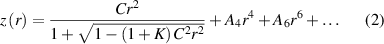
Diffractive lenses were developed to replace the conventional refractive lenses, due to the advantages of light weight, easy to fabricate, cost-effective, and easy to integrate. Fresnel lenses are considered as the pioneers of diffractive lenses, finding broad applications in imaging, beam shaping, solar energy harvesting, etc [109–113]. Akin to Fresnel lenses, Fresnel zone plates (FZPs) composed of zones with halfwave phase delay or blocked transmission are more flattened without blazed curvature. However, either Fresnel lenses or FZP suffer from large field-dependent aberrations or chromatic aberrations (figure 10(a-i) and (a-ii)), which limit their practical applications in imaging. To overcome the drawbacks of Fresnel lenses and FZP, fractal zone plates (FraZPs), a modified FZP with missing zones (figure 10(a-iii) and (a-iv)), were proposed due to the reduced chromatic aberration under white light imaging and the extended depth of field they provided [114, 115]. To further reduce the chromatic aberration and improve the focusing efficiency of FraZPs, the phase-type and multilevel Kinoform FraZPs were developed (figure 10(a-v) and (a-vi)). As shown in figure 10(a-v), the multilevel sub-micrometer features were fabricated using TPL, a powerful technique for photonic devices working in the visible range, especially for intensity type elements like diffractive lenses and 3D photonic elements like photonic crystals [13, 116]. As demonstrated in figure 10(a-v), the efficiency of the four-level phase-type FraZPs reaches 49.0% theoretically and 37.6% experimentally. Meanwhile, the tightly focused spots are shown in figure 10(a-vi) with the capability of high resolution imaging under white light illumination [115].
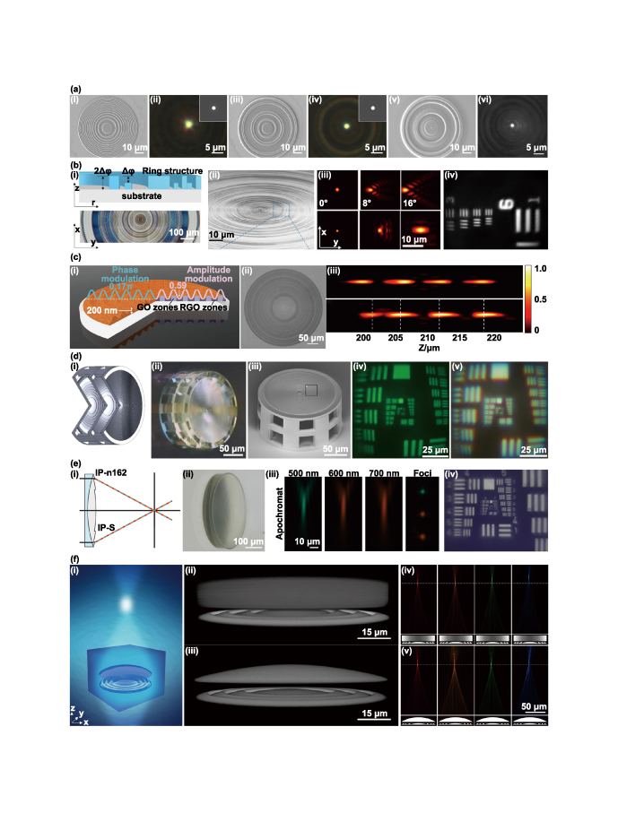
Figure 10. Diffraction lenses fabricated by TPL. (a) Different types of zone plates and their focusing performance. (i)–(ii) SEM image and focal spot of phase-type Fresnel zone plates, the inset is the corresponding simulated focal spot. (iii) and (iv) SEM image and focal spot of phase-type fractal zone plates, the inset is the corresponding simulated focal spot. (v)–(vi) SEM image and focal spot of multilevel fractal zone plates. Reprinted with permission from [115] © The Optical Society. (b) Single-layer aberration-compensate (SLAC) flat lens and its focusing performance. (i)–(ii) Schematic figure of three level phased modulated SLAC flat lens. (iii) The simulated and experimental focal spots under different fields of view. The off-axis aberration is compensated in SLAC flat lens. [117] John Wiley & Sons. © 2020 WILEY-VCH Verlag GmbH & Co. KGaA, Weinheim. (c) Graphene oxide diffractive lenses and its focusing characterization. (i) Schematic of graphene oxide diffractive lenses. (ii) The optical micrograph of graphene oxide diffractive lens. (iii) Simulated and experimental multifocal spots along its optical axis. Reproduced from [130]. CC BY 4.0. (d) 3D printed stacked diffractive achromatic microlenses. (i)–(iii) Schematic, optical micrograph, and SEM of a triplet stacked diffractive lens. (iv) and (v) Imaging of USAF targets under laser or white light illuminations, respectively. Reprinted with permission from [132] © The Optical Society. (e) 3D printed hybrid refractive/diffractive apochromatic lenses. (i) and (ii) Schematic and optical micrograph of hybrid TPL 3D printed diffractive lenses. (iii) Longitudinal and transverse focal spots produced with apochromatic diffractive lenses under different wavelengths. (iv) Imaging-result of USAF targets under white light. Reprinted with permission from [133] © The Optical Society. The Optical Society. (f) Volumetric hybrid achromatic microlenses with high focusing efficiencies. (i)–(iii) Schematic of volumetric hybrid diffractive lenses, GRIN/diffractive lens, refractive/diffractive lens. (iv) and (v) Focal spot characterization of GRIN/diffractive lens and refractive/diffractive lens. Reproduced from [134]. CC BY 4.0.
Download figure:
Standard image High-resolution imageTo achieve wide angle imaging and compensate field-dependent aberrations, a single-layer aberration-compensate (SLAC) flat lens was designed with epsilon-greedy optimization method and fabricated using Nanoscribe [117]. The off-axis aberration is essential for wide angle imaging and becomes one of the biggest challenges for the commercial application of flat lenses. To correct the off-axis aberrations, doublet metalenses were proposed and fabricated on both sides of a transparent substrate [118, 119]. However, the difficulties in doublet metalenses design, requirement of precise alignment, and time-consuming manufacturing processes hinder its further development and practical use [117]. To solve these problems, C Hao and coauthors demonstrated SLAC flat lens with capability of wide FOV imaging, where three level phase modulation was applied (figure 10(b-i)and (b-ii)). The off-axis aberration was compensated along the focal plane and a 2.2 µm monochromatic imaging resolution was achieved within the FOV of 32° (figure 10(b-iii) and (b-iv)).
Besides FOV, NA also plays an important role in high resolution imaging, the Abbe diffraction limit of flat lenses is inversely proportional to its NA. The large-scale and high-NA are difficult to reach simultaneously for metalenses and conventional diffractive lenses [120, 121]. Meem et al overcame this problem using multilevel diffractive lenses (MDLs) with large diameter of 4.13 mm and high NA of 0.9 working at the wavelength of 850 nm [122]. Furthermore, the chromatic aberration can also be corrected through inverse design and MDL, achieving broadband focusing in both visible and infrared ranges [123–126]. The imaging resolution of such MDLs is comparable to metalenses and the focusing efficiency is even higher with the standard optical characterization metric [6, 127–129].
In addition to multiple phase steps, the amplitude also contributes to control complex light field. Both together form complex amplitude of light, offering a more sophisticated control of incident beams and higher focusing efficiency for flat lenses [85, 130]. Based on the complex amplitude modulation of incident beam, ultrathin flat diffractive lenses can be realized producing well-defined focal spots, such as multiple focal spots along the optical axis and optical needles [130]. As shown in figure 10(c-i) and (c-ii), the ultrathin graphene oxide films (∼200 nm) are modulated in both phase and amplitude when exposed to the femtosecond laser beam. The reduced graphene oxide together with its sinusoidal profiles in the reduced region provides 0.17π phase delay and decrease in amplitude. To realize multifocal spots and optical needle, the convex optimization method is applied with desired target functions. Both simulated and experimental results show the desired multiple focal spots and optical needles, based on the large-scale fabricated graphene oxide diffractive lenses (∼350 nm) with NA of 0.64 (figure 10(c-iii) and (c-iv)). Notably, multifocus diffractive optical elements in the form of phase-only holograms have been created on the end face of optical fibers using TPL [131]. Besides creating multiple foci in two image planes, the phase of adjacent foci could be controlled, representing a novel pathway to excite complex resonant modes in nanophotonics or fiber optics.
Benefiting from the TPL 3D printing, diffractive lenses with complex 3D structures can be fabricated at once, namely stacked diffractive lenses or hybrid diffractive lenses [70, 132, 133]. The field related aberrations of flat lenses degrade imaging quality especially in the case of high NA or large FOV. Stacked diffractive lenses (figure 10(d-i), (d-ii) and (d-iii)) promise to solve this problem by combining doublets or triplets of diffractive lenses together [132]. This technique enables sub-micrometer imaging resolution with a full FOV of up to 60° and compensates focal spots from oblique incident angles to the same focal plane [132]. Imaging capabilities with monochromatic laser illumination and white light illumination are exhibited as shown in figure 10(d-iv) and (d-v). On the other hand, chromatic aberration can be compensated for when incorporating photo resins with different Abbe numbers, i.e. hybrid diffractive lenses. As shown in figure 10(e-i) and (e-ii), the hybrid diffractive lenses are composed of a concave lens with IP-n162 and diffractive lenses made of IP-S, fabricated using Nanoscribe [133]. The apochromatic hybrid diffractive lens corrects focal spot displacement and secondary spectrum displacement as designed (figure 10(e-iii)). Corresponding imaging capability under white light illumination is verified using United States Air Force (USAF) test targets without obvious color seams.
A special hybrid diffractive lens within a host medium is shown in figure 10(f), the polymetric structure made of IP-dip is fabricated within the pores of a silicon dioxide (PSiO2) locally replacing the air in the pores [134]. Due to the volumetric nature of the hybrid diffractive lens, it is quite mechanically robust with the thickness of only 15 µm. Two types of hybrid lenses, gradient RI (GRIN) lens combined with diffractive lens (figure 10(f-ii)), and refractive lens combined with diffractive lens (figure 10(f-iii)), both show corrected focal spots under different wavelengths with high focusing efficiencies (figure 10(f-iv) and (f-v)).
4.3. Metalens
Metalens is an advanced flat optical device which consists of artificially engineered sub-wavelength structures [135]. Recently, the characteristics of ultra-compact, ultra-thin, more degrees of design freedom and good ability to manipulate light have made metalens compelling in imaging optics [5]. Metalens has multiple advantages over diffractive lens. The main difference between metalens with traditional diffractive lens is the nonconventional phase accumulation, which is due to the discrete sub-wavelength structures. Thus, high-resolution fabrication methods like electron beam lithography and photolithography are required to prototype the metalens in 2D or 2.5D. However, with the development in the research of metalens, a 3D printing and faster fabrication method is needed to realize the more complicated design which can achieve a better performance. TPL is able to manufacture the structures from 1D to 3D and maintain the sub-wavelength resolution in one fabrication step. For imaging devices from 2D to 2.5D, TPL is extremely convenient and fast. Through the fine-tuning of the fabrication parameters including scanning speed and laser powers, TPL is promising to print the sub-wavelength structure that works in a large range of wavelengths [136]. Hadibrata et al utilized the Nanoscribe to print lines with different laser powers of 6 mW, 7 mW, 8 mW, and 9 mW. The smallest line width is measured to be about 220 nm. They inversely designed the metalens and 3D printed on a fiber tip, as shown in figure 11(a) with the focal length of ∼8 µm and the focal spot at the size of ∼100 nm. This approach can be utilized for two-photon direct laser lithography, enhancing the performance [137]. Roques-Carmes et al introduced a methodology for the reverse engineering of multilayer metaoptics through topology optimization. This method involves using multiple, densely arranged layers of a low-index polymer, allowing multilayered metaoptics to attain high-efficiency multifunctionality. As shown in figure 11(b), the minimum structural size was designed to be 310 nm [138]. Duan et al developed a supercritical lens with a single-layer structure, specifically designed to compensate for aberrations. They experimentally demonstrated the supercritical lens, possessing an NA value of 0.63, was capable of achieving sub-diffraction limited focusing in the far-field within a 20° FOV, at the wavelength of λ = 633 nm. The minimum feature size was set as 200 nm and there are eight height levels of the rings along the light propagation direction [139]. Christiansen et al innovated new axisymmetric inverse design methods that address challenges distinctly different from those of conventional lenses, such as creating reconfigurable lenses. In their research, they also limited the radial design pixel size to a minimum of 200 nm. They provided experimental validation for an axisymmetric, inverse-designed, monochrome lens tailored for the NIR spectrum, which was fabricated using TPL (figure 11(c)) [140]. Due to the resonance in the nanoscale, in the previous works, efficient and accurate electromagnetic calculation methods and time-saving inverse design algorithms are necessary to develop multi-functional and better performance metalens. Except for the 2.5D metalens or supercritical lens which is built of circular lines, 2D metalens consisting of sub-wavelength meta-atom is also manufacturable. Plidschun et al and Ren et al took advantage of the flexibility on fabrication substrates, they fabricated the metalens on the fiber to extend the application scenarios. Ren et al introduced the design and nanoprinting of a 3D achromatic metalens on the tip of an SMF. This metalens is adept at achieving achromatic and polarization-insensitive focusing throughout the entire NIR telecommunication wavelength spectrum, which spans from 1.25 μm to 1.65 μm (figure 11(d)) [72]. Plidschun et al executed the fabrication of an ultrathin metalens on the surface of a modified single-mode optical fiber using direct laser writing. This resulted in a diffraction-limited focal spot with a record-setting high NA of approximately 0.9 (figure 11(e)) [71]. When the desired performance and degrees of design freedom are limited to a single layer, researchers designed hybrid or multi-layer metalenses to obtain better performance imaging devices. Balli et al demonstrated a new type of hybrid metalens (phase plate at the bottom and a metalens above the phase plate) to achieve broadband focusing ranges from 1000 nm to 1800 nm (figure 11(f)) [141], a 3D achromatic metalens with ultrabroadband capabilities, functioning from the visible spectrum to the shortwave infrared, 450–1700 nm, 200 μm diameter and 0.04 NA [142] and rotationally tunable varifocal 3D doublet metalenses working at the wavelength of 1500 nm [109], respectively. Another important advantage of TPL demonstrated here is that there is no collimation problem between layers and the multi-layer structure can be fabricated in a single step.

Figure 11. Metalens fabricated by TPL. (a) SEM image of the manufactured lens on the tip of a single-mode fiber. Reprinted with permission from [137]. Copyright (2021) American Chemical Society. (b) Top-view SEM images reveal the upper layer consisting of straight polymer lines, the smallest of which have a feature size of 310 nm. Beneath this lies another layer, obscured by an unpatterned segment with a thickness of 930 nm. Reprinted with permission from [138]. Copyright (2022) American Chemical Society. (c) SEM of the full 3D printed single-layer circular symmetric supercritical lens. Reprinted with permission from [139] © The optical Society. (d) SEM image of the 3D nanoprinted achromatic metafiber. Reproduced from [72]. CC BY 4.0 (e) SEM image of the metafiber with an ultrahigh NA metalens. Reproduced from [71]. CC BY 4.0. (f) SEM images showcasing a 40 μm diameter hybrid achromatic metalens, characterized by an air-spaced design with a 0.32 NA, which was fabricated on fused silica substrates. Reproduced from [141]. CC BY 4.0.
Download figure:
Standard image High-resolution imageIn a short summary, except for the refractive and diffractive imaging devices, TPL is promising to fabricate sub-wavelength metalens working from visible range to infrared, even longer wavelength. Besides, the 3D printing ability also provides more opportunities to manufacture imaging devices on various substrates and allows researchers to explore more complicated structures including hybrid lens or multi-layer imaging devices, which offer more degrees of freedom to achieve better performance and more optical functions. There are still some limitations for metalens via TPL currently. In the reported TPL metalens works, the smallest feature size is limited to ∼200 nm, which constrains the design capacity for shorter wavelength. Besides, a relatively low RI material is unavoidable, which does not have strong abilities to manipulate light compared to commonly used materials for metalens, e.g. TiO2, GaN and Si. However, the advantages of TPL, including the convenient and fast fabrication process, manufacturable 3D structures and flexible printing substrates, make metalens fabricated via TPL have more potential to excavate.
4.4. Gradient index lens
In the traditional lenses, the RI of the lens is usually constant. Nevertheless, it is feasible to fabricate lens elements with a continuously varying index of refraction throughout the material. These types of lens elements are referred to as gradient-index (GRIN) components [143]. Commonly, the GRIN elements are fabricated by chemical vapor deposition [144], neutron irradiation [145], partial polymerization [146], ion exchange [147] and diffusion-assisted lithography [148]. However, they all lack the ability to make GRIN elements in arbitrary shape. With the rapid development of TPL, researchers explore materials and mechanisms to extend the application scenarios of TPL. Žukauskas et al studied the determination of the interplay between DC and RI of the structures by changing the laser intensity and scanning velocity. In their work, they found the decrease of the Irgacure 369 photoinitiator, the stretching mode of the C=C bond in the cross-linking methacrylate group and the stretching mode of the carbonyl group in response to increased laser power (figure 12(a)). Based on average values of the dielectric constant as a function of the average power intensity of the writing laser beam and the scanning speed in figure 12(b), it tells that by controlling the laser power and scanning speed, they can tailor the RI to fabricate the GRIN trapezoidal prism [40].
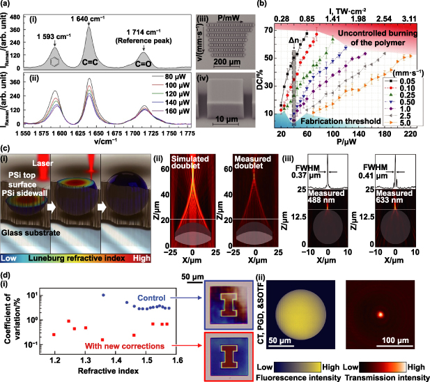
Figure 12. Fabrication mechanism and applications of gradient index imaging devices via TPL. (a) Raman spectrum of photoresist SZ2080 and the structures fabricated with varied laser powers at a constant velocity. (i) Raman spectrum of the pre-polymer. (ii) Evolution of the Raman spectra for cuboids produced at a speed of 2.5 mm·s−1. (iii) SEM images showing a series of cuboids created using TPL, and (iv) an enlarged view of one of these cuboids at a 45° angle for detailed observation. (b) Experimental data for the DC as a function of the TPL average laser power/intensity and scanning velocity obtained from three independent measurements. (a), (b) [40] John Wiley & Sons. © 2015 by WILEY-VCH Verlag GmbH & Co. KGaA, Weinheim. (c) Spherical Luneburg lens. (i) Conceptual illustration depicting the creation of a spherical Luneburg lens 3D-printed within PSi, featuring an adjustable subsurface refractive index achieved through the beam exposure technique. (ii) Comparative data on the simulated and actual light propagation for the doublet at a wavelength of 633 nm. (iii) Documented intensity profiles on the xz-plane of Luneburg lenses fabricated in PSi, focusing light at wavelengths of 488 nm and 633 nm on their surfaces, yielding FWHM values of 0.37 and 0.41, respectively. Reproduced from [149]. CC BY 4.0. (d) High-precision GRIN lens for fluorescence imaging. (i) Comparison of the color camera images of pattern 'I' before and after conducting higher precision GRIN control. (ii) Fluorescence photographs (left) and 642 nm microscopic images (right) of axicons with corrections. Reproduced from [151]. CC BY 4.0.
Download figure:
Standard image High-resolution imageFor GRIN elements, there exist three types of index-of-refraction gradients, axial gradient, a radial or cylindrical gradient and spherical gradient. One important example of the spherical gradient which should be noted is the Luneburg lens. Ocier et al presented a new way to print the volumetric GRIN Luneburg lens. They control the subsurface RI via the beam exposure (SCRIBE). In figure 12(c-i), it demonstrates DLW within nano porous silicon (PSi) and silica scaffolds filled with photoresist, allowing for the adjustment of the RI over a range exceeding 0.3. They first prototyped the doublet to realize the chromatic dispersion control, as shown in figure 12(c-ii). Furthermore, a Luneburg lens was also successfully created, a type of lens that is free from aberrations and coma, characterized by its spherically symmetric RI profile, as shown in figure 12(c-iii). Using the proposed SCRIBE technique, they enhanced the capabilities of TPL fabrication by merging the geometric precision of TPL with an efficient medium materials platform. It enables the simultaneous definition of the index in 3D and volumetric shapes [149]. Besides, Porte et al incorporated light exposure as an extra dimension in the process of 3D laser writing. They successfully produced GRIN volume holograms and waveguides with pre-defined RI profiles [150]. Littlefield et al presented further modifications to the GRIN control to enable higher uniformity. They conduct three modifications: (1) adjusting the planar write field of mirror galvanometers by employing a spatially varying optical transmission function, which compensates for large-scale optical aberrations; (2) regularly repositioning the piezoelectrically driven stage, a technique known as piezo-galvo dithering, to minimize small-scale writing errors and (3) maintaining a consistent duration between each lateral cross-section to decrease variations throughout the entire writing depth [151]. After the corrections we can see obviously better control GRIN, as shown in figure 12(d-i). They increase the index difference range to 0.37 and decrease the standard deviation from 0.13 to 0.0021. In addition, they experimentally demonstrated the fully corrected axicon which performed as they have designed. Due to the limitation of the materials, few works of GRIN lens by TPL have been studied so far. The investigation of new materials with low absorption and higher RI ranges can provide more potential in the future.
4.5. Lens arrays, compound lens, and light field imaging
A microlens array (MLA) comprises many individual microlenses packed together in a certain order for advanced functionalities. Three important fabrication requirements of MLAs are low surface roughness, high fill factor (i.e. packing density), and high array uniformity. TPL is useful in the fabrication of MLAs because it enables rapid prototyping of customized design, while satisfying the fabrication requirements.
The first requirement of low surface roughness is to minimize light scattering and optical losses. To fabricate MLAs with low surface roughness, Chung et al demonstrated an improved vertical slicing method over the conventional horizontal slicing method [152]. In addition, Aderneuer et al demonstrated that freeform micro-optical arrays fabricated by two-photon grayscale lithography had lower areal roughness (10 nm) than those fabricated by conventional TPL (29 nm) [153]. Yan et al demonstrated another technique via 3D focal field engineering to fabricate a continuous surface Fresnel MLA [154]. Kotz et al demonstrated post-processing an MLA made of two-photon curable silica nanocomposite resin through thermal debinding and sintering to achieve a surface roughness of 6 nm [46]. Liu et al demonstrated a self-assembly-based mold-free approach of mass-production of scalable MLAs, with ultrasmooth surface (roughness of around 0.3 nm), ultrahigh resolution, and large variable curvatures [155]. The second requirement of a high fill factor is to maximize the light collection efficiency. To fabricate MLAs with high fill factor, the microlenses are typically packed in square or hexagonal arrays. Based on simple geometric calculations, the highest fill factor for microlenses with circular apertures is around 79% in a square array and 91% in a hexagonal array. However, up to 100% fill factor can be achieved for microlenses that have square or hexagonal apertures, respectively. Niu et al demonstrated close-packed square and hexagonal multilevel FZP arrays with diffraction efficiency of up to 75% for imaging (figure 13(a)) [156]. Furthermore, Huang et al showcased a hexagonal MLA with a 100% fill factor and 92% focusing efficiency. This MLA was utilized as a Shack–Hartmann wavefront sensor, enabling the detection of obliquely incident beams and vortex beams [157]. The third requirement of high array uniformity is to ensure consistent optical performance across all microlenses. To fabricate MLAs with high uniformity, parallel processing techniques have been used. Yang et al demonstrated a multi-foci TPL system based on a spatial light modulator to fabricate hemispherical MLAs with focal spot intensity uniformity of 83% [158]. Similarly, Hu et al demonstrated a holographic femtosecond laser processing technique to fabricate aspherical MLAs with an improved focal spot intensity uniformity of 97.6% by compensating for nonideal properties of the spatial light modulator [159].
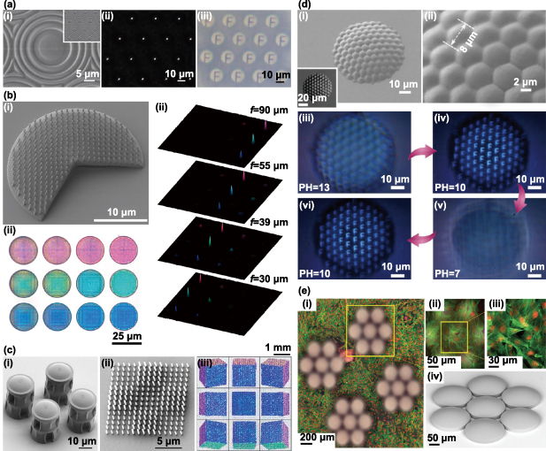
Figure 13. Microlens arrays (MLAs) fabricated by TPL. (a) Hexagonal Fresnel zone plate. (i) SEM image of a hexagonal Fresnel zone plate array with 100% fill factor. Optical micrographs of (ii) focal spots, and (iii) clear images 'F' formed by the array. Reprinted from [156], Copyright © 2010 Elsevier B.V. All rights reserved. (b) Structural color-filtered microlens. (i) SEM image of a color-filtered microlens comprising a base plate, shell structure, and nanopillars. One slice of the lens has been cut out for illustration purposes. (ii) Optical micrograph of a color-filtered microlens array with spatially varying focal lengths f. (iii) 3D surface topography of colorful focal spots imaged at different planes. The cone colors represent the focal spot colors, and the cone heights represent intensities. Reprinted with permission from [162]. Copyright (2021) American Chemical Society. (c) Light field print with integrated structural color pixels and microlenses. (i) SEM image of a sub-array of 2 × 2 display units in a light field print. Each display unit consists of a microlens supported by a tower above a block of structural color pixels. (ii) SEM image of structural color pixels that comprise nanopillars with varying heights. (iii) Digital camera images of a light field print that displays changing perspectives of a multi-colored cube across a range of observation angles. Reproduced from [163]. CC BY 4.0. (d) Smart compound eye (CE) with a variable focal length. (i) Low-magnification SEM image of a smart compound eye fabricated on a hemispherical curved surface. (ii) High-magnification SEM image of the CE. (iii)–(vi) Optical micrographs showing variable focal length of the CE when immersed in solutions with different pH values. [166] John Wiley & Sons. © 2019 WILEY-VCH Verlag GmbH & Co. KGaA, Weinheim. (e) MLAs for confocal imaging. (i) Confocal image of stained human fibroblasts superimposed with MLAs. (ii) Full FOV fluorescence confocal image through an MLA. (iii) Cropped scan area through a single microlens. (iv) SEM image of the MLA. Reproduced from [169]. CC BY 4.0.
Download figure:
Standard image High-resolution imageAfter MLAs are fabricated by TPL, their physical structures and optical properties are typically fixed. To overcome this limitation, He et al demonstrated a liquid crystal (LC) MLA with dynamically tunable focal length in response to different applied voltages [160]. On the other hand, a static MLA can comprise microlenses with spatially varying focal lengths to form a curved image plane, as demonstrated by Tian et al [161]. In a similar yet unorthodox fashion, Wang et al demonstrated 'optical fireworks' transmitted from sparsely arranged color-filtered microlenses with four different focal lengths to form colorful focal spots that appear and disappear at different image planes (figure 13(b)) [162]. MLAs fabricated by TPL have also been used for light field imaging, in which Chan et al demonstrated a 65 × 65 MLA integrated with structural color pixels to display changing perspectives of a 3D image across a range of 32° observation angles (figure 13(c)) [163]. Inspired by optical systems in nature, MLA-based CEs have also been engineered to improve the FOV, resolution or bandwidth. Lin et al demonstrated artificial CEs by designing an MLA on a curved substrate to achieve a much wider FOV (107.48° × 97.97°) than a planar MLA (36.52° × 36.52°) [164]. Similarly, Hu et al demonstrated an optoelectronic CE camera for distortion-free, wide FOV (90°) imaging [67], and Dai et al demonstrated a biomimetic apposition CE for full-color, wide-angle panoramic imaging [165]. Ma et al further demonstrated smart CEs with tunable FOV (35°–80°) and variable focal length (246–362 μm) to simultaneously mimic insect and human eyes (figure 13(d)) [166]. Aside from CEs, Schäffner et al demonstrated a spherical MLA to generate multiple optical tweezers patterns that are individually controlled by spatial light modulation from a digital micromirror device [167, 168]. Moreover, Marini et al demonstrated MLAs for non-linear excitation microscopy of biological samples and in-vivo inspection of cellular dynamics (figure 13(e)) [169]. Finally, MLAs fabricated by TPL have been used for spectroscopic measurements, where Bogucki et al demonstrated aspherical MLAs on single light emitters such as quantum dots and van der Waals heterostructures [170]. Dietrich et al demonstrated freeform lens arrays on multi-core fibers to achieve light coupling with up to 73% efficiency in astronomical instruments [171]. Though TPL is a versatile technique for fabricating MLAs with precise shapes that require low surface roughness, high fill factor, and high array uniformity, its serial patterning process is too time consuming and expensive for reproducing multiple copies of the same MLA. Hence, a proposed strategy for mass production is to fabricate a master mold of the MLA by TPL, and then duplicate the lenses by using nanoimprint lithography [172] or roll-to-roll processes [173].
4.6. Dynamic lenses
Static lenses have been used in many studies on microoptical elements as exhibited above, while a dynamic lens is required to implement new functions or apply them to specific scenarios for light control with an external stimulus [174]. Combining static lenses with dynamic responsive materials, such as electric field-responsive LCs or microfluid channels for flowing liquid, is a commonly used method to change the local RI, thereby modulating the focal length and spatial phase. Recently, Wu et al reported an LC phase modulator with tunable properties using the TPL technique [160, 175]. The LC MLA exhibited unique modulation functions, in which the focal length and phase profiles were tuned by varying the applied voltage. The LC molecule mixture was placed between the MLA and another indium tin oxide substrate with a rubbed polyimide layer, whose total cell functioned as a composite lens, as shown in figure 14(a). Interestingly, the surface of the microlens had a small groove shape because it was exposed and printed using the raster scan of a 780 nm pulse laser (figure 14(a)). The periodic asperities facilitated an anchoring force on the LC molecules along the direction of the groove. They further reported that the diffraction effect generated by the grooves was negligible, because the period of the grooves was longer than the wavelength in the visible range. Therefore, the assembled LC microlens cells exhibited sufficient transparency. When a cell voltage greater than 1.5 V was applied, the focal length increased and finally functioned as a convex lens, thus indicating that the images were real and inverted (figure 14(b)). In addition, the phase profiles with aberrations depend on the applied voltage owing to the pretilt angle effect of the LC molecules. They also investigated and demonstrated the capability of the assembled LC microlens cell using letters and imaging targets, which showed clear images (line pair with a resolution of 57.0 lp mm–1).

Figure 14. Dynamic lens fabricated with TPL. (a) Schematic of the LC microlens cell and SEM images of the microlens. (b) Imaging target under white light as a function of the applied voltage. (a), (b) Reprinted with permission from [160]. © The Optical Society. (c) Comparison of conventional single-layer M-DOE and multilayer M-DOE. (i) Conceptual schematic of the structure design of conventional single-layer M-DOE and (ii) broad-bandwidth multilayer M-DOE. (d)–(f) Optofluidic-integrated M-DL and SEM and laser scanning confocal microscopy images. (c)–(f) [177] John Wiley & Sons. © 2021 Wiley-VCH GmbH.
Download figure:
Standard image High-resolution imageMicrodiffractive optical elements are widely used for integrated optical systems [117, 176] as they can easily control the propagation path, that is, the phase shift of the incident light field. However, they only work in a narrow bandwidth to achieve highly efficient first-order diffraction. If a different wavelength is used, the diffraction efficiency decreases because of the generation of a diffraction with different orders of magnitude. Hu et al demonstrated a high-efficiency and broad-bandwidth diffractive three-layer lens containing polymeric blazed gratings and a fluidic RI-matched layer, as shown in figure 14(c) [177]. They optimized the materials and heights of the micro-diffractive structures using the Schott dispersion formula. Note that the shapes of micro-diffractive structures and materials can be easily modified using the TPL technique. Subsequently, the curved and diffractive surfaces of the lenses were printed with high precision and accuracy. Finally, SU-8 photoresist for both the top and bottom media and glycol for the intermediate media were selected. The incident light was diffracted to the same order over a wide visible range, and the average diffraction and focusing efficiencies exceeded 80%. The capability of the microdiffractive lens with microfluid channels was evaluated using an optical imaging test with a microscope, obtaining clear and high-resolution images under different wavelengths (line pair with a resolution of 91.0 lp mm–1), as seen from figures 14(d)–(f).
There is a strong demand for dynamic lenses that can modulate light in a precise and reconfigurable way currently. Besides, other stimuli, such as thermal, magnetic, and pressure stimuli, could also be used in the future. With high-quality and high-speed modulation achieved, TPL printed dynamic lenses can be applied in many fields, such as integrated quantum photonic technology, virtual/augmented reality, drones, and smartphone devices.
4.7. Endoscopic imaging
The first modern endoscope was introduced in the early 19th century [181], which has evolved as one of the most useful imaging modalities in multiple medical disciplines. Endoscopes enable structural and molecular measurements in vivo, offering a powerful microscopic imaging tool for diagnosis of pathological changes associated with disease and inspection of inner cavities of the human body. Flexible endoscopes, with the thickness in the same order as human hair, can be inserted into blood vessels to provide high quality 3D images. Clinical diagnostics nowadays increasingly rely on endoscopic techniques to visualize internal organs at a high resolution. This helps scientists better understand the causes of heart attacks and could lead to improved treatment and prevention. Therefore, miniaturization of endoscopic probes becomes necessary for imaging small luminal or delicate organs without causing trauma to tissue. This section gives an overview of the state-of-the-art micro-endoscopes interfaced with 3D micro-optics or ultrathin metasurfaces, some of which were directly fabricated on the end faces of optical fibers using TPL.
Traditional methods for creating highly miniaturized endoscopic probes often face limitations, leading to undesirable spherical aberration, reduced resolution, or limited depth of focus [178, 179, 182, 183]. Miniature endoscopes, particularly those employing optical coherence tomography (OCT), have typically been constructed by either piecing together probes using sequential micro-prisms and micro-lenses [184, 185] or by attaching gradient-index lenses or ball lenses [186, 187] to the termini of optical fibers. However, the specific index profiles of gradient-index lenses and the particular shapes of ball lenses tend to introduce spherical aberrations, diminishing the imaging capabilities of these endoscopic tools. Furthermore, the specific geometric configurations and index profiles of these lenses often lead to pronounced group delay, which remains uncorrected, causing substantial chromatic aberration that blurs optical images across a broad wavelength spectrum [72]. Only recently has the ability to manipulate chromatic dispersion in imaging lenses mounted on the ends of optical fibers been achieved through the use of an achromatic metalens [72] or a reverse-engineered metalens [180], applied directly to fibers for broadband imaging applications.
Achieving both high-resolution imaging and extensive depth of focus is challenging in endoscope design, especially when using traditional optical methods. To address this challenge, Li et al introduced an innovative technique for creating ultrathin probes. This method involves 3D microprinting to consistently produce side-oriented freeform micro-optics (less than 130 µm in diameter) on SMFs (illustrated in figure 15(a)) [178]. Employing this approach, they successfully constructed a fully operational, ultrathin probe specifically corrected for optical aberrations for OCT use. Remarkably, the diameter of this freeform endoscopic probe, including the catheter sheath, is just 0.457 mm. Li et al showcased its high-quality 3D imaging capabilities and mechanical adaptability by conducting imaging on atherosclerotic arteries in humans and mice [178]. The development of this compact OCT catheter paves the way for groundbreaking minimally invasive medical applications in diagnosing and monitoring diseases.

Figure 15. Multiple miniaturized endoscopic probes fabricated with TPL. (a) The endoscopic system's optical configuration includes light emerging from a single-mode fiber, widening in a no-core fiber for beam expansion, undergoing reflection and phase alteration at the freeform mirror, traversing the catheter sheath, and then concentrating into the artery tissue. In the bottom left: a microscopic view of the 3D laser-crafted total internal reflection mirror at the apex of the no-core fiber, which is fused to a single-mode fiber. On the right: an image of the 3D laser-fabricated endoscope. Reproduced from [178]. CC BY 4.0. (b) A broadband achromatic metafiber designed for precise focusing and imaging throughout the complete telecommunication spectrum. On the left: SEM image of the achromatic metafiber. In the middle: experimentally determined point spread functions of the achromatic metafiber in both the longitudinal (left) and lateral (right) dimensions at five distinct wavelengths of 1250 nm, 1350 nm, 1450 nm, 1550 nm, and 1650 nm. On the right: a diagrammatic representation of the optical arrangement utilizing an achromatic metafiber to produce sharp, in-focus visual responses under broadband light conditions. Reproduced from [72]. CC BY 4.0. (c) Schematic of the nano-optic endoscope, in which the metalens was designed to image a point source to a diffraction-limited focus with a working distance of 0.5 mm. Top left: optical image of the distal end of the nano-optic endoscope. Bottom left: SEM image of a portion of a fabricated metalens. Reproduced from [179], with permission from Springer Nature. (d) Schematic of the meta-optic fiber endoscope: meta-optics are optimized to possess a large average volume across a broad wavelength range to preserve colors. Compared to a traditional GRIN lens, the utilization of metalens reduces the tip length while maintaining a wide field of view of 30° and a large depth of field exceeding 30 mm. Reproduced from [180]. CC BY 4.0.
Download figure:
Standard image High-resolution imageEngineering dispersion is crucial for the effectiveness of most contemporary optical systems, including those involving fiber optics. While the chromatic dispersion in a meter-long SMF typically used in endoscopic tools is minimal, the optical lenses placed at the fiber's end face for focusing and imaging are prone to significant chromatic aberration. Ren et al introduced the concept and fabrication of a 3D achromatic diffractive metalens at the end of an SMF. This metalens is designed for achromatic and polarization-neutral focusing throughout the entire NIR telecommunication wavelength range of 1.25 µm–1.65 µm (shown in figure 15(b)) [72], encompassing the entire spectrum utilized by standard SMF-28 fibers.
Additionally, they showcased the use of this compact and adaptable achromatic metafiber in fiber-optic confocal imaging, producing sharp, in-focus images under a wide range of light illumination [72]. The achromatic metafiber excels in generating in-focus images under broad spectrum light illumination across the telecommunication range, achieving a spatial resolution as fine as 4.92 µm. These findings indicate that 3D meta-optics not only miniaturize endoscopic imaging systems but also broaden their wavelength range, ensuring high-quality images under various light conditions. The employment of longer wavelengths in the NIR spectrum enhances image clarity due to significantly reduced photon scattering and autofluorescence. Consequently, this achromatic metafiber can be applied in distal-scanning endoscopes for practical imaging, where a fiber-based beam splitter could separate excitation and fluorescence signals in fluorescence imaging.
Pahlevaninezhad et al developed an endoscopic OCT catheter incorporating a metalens. This metalens, made of amorphous silicon-based nanopillars with subwavelength sizes, is a key component in their nano-optic endoscope, facilitating near diffraction-limited imaging as shown in figure 15(c) [179]. The precision in phase control and high spatial resolution of metalenses eliminate spherical aberration and astigmatism, thereby addressing critical obstacles in achieving diffraction-limited focus and imaging. They successfully employed this technology for endoscopic imaging in both human lung tissues removed during surgery and live sheep airways [179]. The subwavelength-scale efficient and adaptable light manipulation offered by the metalens approach simplifies the process of achieving high-quality focus and imaging, eliminating the need for complex designs and assembly of optical components. When compared to conventional GRIN lens catheters and ball lens catheters, the nano-optic endoscope with its metalens demonstrates superior capabilities. Its effectiveness in capturing high-resolution images of subsurface tissue structures in vivo significantly enhances the potential clinical applications of OCT for disease detection, diagnosis, and monitoring. It is, however, important to note that the metalens used in this setup does experience substantial chromatic aberration, which can restrict its effectiveness in broadband operation.
Fröch et al reported an inverse-designed meta-optic fiber endoscope integrated with a 1 mm diameter coherent fiber bundle, resulting in a 33% decrease in the rigid tip length compared to traditional GRIN lenses (figure 15(d)) [180]. They demonstrate a meta-optic fiber endoscope for capturing real-time video in full visible color. The meta-optic enables operations at a field of view of 30°, a depth of focus of >30 mm (exceeding 300% of the nominal design working distance) and a minimum rigid tip length of only ∼2.5 mm. To achieve a good compromise of transverse resolution, depth of focus, field of view, and full-color performance of the meta-optic fiber endoscope, they employed the inverse design approach to optimize all these figures of merit, wherein an automatic differentiation framework was used to iteratively adapt the volume of a multichromatic MTF [180]. They positioned an organic light-emitting diode (OLED) screen at the proximal end of the fiber bundle in front of the meta-optic, and at its distal end, they installed a capturing system comprising an objective, tube lens, and camera. A series of multicolored images were displayed on the OLED screen and captured via the fiber bundle. Remarkably, the color fidelity remained intact across the entire visible spectrum, even for intricate scenes, despite the metalens not being directly fabricated on the fiber bundle.
To summarize, recent advancements in endoscopic probe designs, in contrast to those relying on traditional micro-optical elements like lenses and prisms, have led to the development of probes that are notably smaller, ultra-slim, and possess free-form characteristics [178–180, 183]. These innovative features facilitate secure access to delicate and hard-to-reach internal organs, ensuring both high-resolution and aberration-free imaging through fibers. It is anticipated that the enhanced high-resolution intravascular imaging provided by these advanced probes could yield essential microstructural details crucial for diagnosis and treatment guidance. Besides, we have witnessed that 3D laser printing technology based on TPL has offered a powerful platform to implement endoscopic probes with on-demand photonic functions and improved imaging performance. In this context, 3D-printed micro-optics with flexibly designed free-form refractive optical elements could largely facilitate high quality fiber imaging and aberration correction [66, 69, 70]. In addition, metafibers (interfacing metasurfaces with the end face of an optical fiber) have recently emerged as a new platform to arbitrarily transform the fiber outputs [188], which can largely enrich the fiber functionalities that cannot be realized from 3D-printed refractive optical elements. For instance, metafibers have the capacity of manipulating the fiber output in multiple degrees of freedom of light, including not only the amplitude and phase, but also the polarization and dispersion of guided fiber modes [71, 72, 188]. The great flexibility of 3D laser nanoprinting opens the possibility of interfacing 3D-printed free-form micro-optics with ultrathin metafibers. We believe these complementary photonic platforms will further facilitate the implementation of new miniature endoscopes that can push the imaging performance to a previously unseen level.
4.8. Computing imaging with diffractive optical neural network
Deep neural networks (DNNs) are data structures that are inspired by the layout of biological neurons. They consist of layers of interconnected nodes that can learn from data and perform various tasks, such as image recognition, natural language processing, and speech synthesis. DNNs is the core technology behind the emerging AI like AlphaGo and generative pre-trained transformer (GPT), especially the latest version of GPT and related AI accomplishments. After training with large amounts of parameters and data, they exhibit their capability and possibility in a wide scope. It bridges human and machine by imparting 'memory' and 'knowledge' to machine and let them be 'smart' enough to understand human language and help solve complex problems. AI now can generate natural language text, algorithm codes for tasks depicted in natural language, and even create images from text captions. It is so powerful that almost for certain this technology will deeply shape our future world and bring revolutions to many fields in science and technologies. The initial idea of neural networks dates back to the 1940s [189]. The development was slow in the first decades [190]. Major breakthroughs came in the 1980s, when new algorithms like backpropagation and other architectures were developed [190, 191]. The fast development started in the 1990s and 2000s witnessed further advances and applications of neural networks in various domains, such as speech recognition, natural language processing, computer vision, and reinforcement learning. Until the 2010s, DNNs became widely popular and influential. The big leap occurs in the past 5 years, thanks to the availability of large-scale data sets, powerful computing resources, and novel machine-learning techniques. However, the fast-growing AI demands for large scale DNNs, which need tremendous amount of time and computational energy cost [31].
Optical DNNs or diffractive DNNs (DDNNs) is one of the promising candidates due to the intrinsic advantages of using light [192–195]. More specifically, the matrix-vector multiplication, which is the dominant calculation task in DNNs, can be achieved in Fourier optics with the speed of light [196, 197]. In addition, the optical matrix-vector multiplication process in the optical process costs lower energy compared with the electronic counterpart [198]. Ozcan's research group proposed DDNNs in 2018 [192]. The schematic of the design is shown in figure 16(a), it consists of multiple transmissive (or reflective) layers that act as artificial neurons with complex-valued transmission (or reflection) coefficients. In each layer, the phases and amplitudes are learnable parameters that can be adjusted during the training of DDNNs using error backpropagation and gradient descent algorithms. It can eventually perform specific machine-learning tasks, such as image classification (figure 16(a) top), digit recognition (figure 16(a) bottom). Notably, the large-scale five-layer design of the trained models was then conveniently 3D laser printed [192]. The experimental results show high accuracy and energy efficiency compared to conventional electronic neural networks.
Figure 16. Schematic and conceptual illustration of diffractive optical neural network. (a) Top: diffractive neural networks functioning as a classifier. Bottom: diffractive neural networks functioning as an imaging lens. The layers (d1, d2 ...) in the schematics are phase modulated transmission/reflection layers that have been trained to perform corresponding classifier and lens functions. (b) Chip integrated diffractive neural network by 3D laser printing. Top: the integration schematics. Bottom: the SEM (left and right) and optical (middle) images of the device. The bottom left and middle images are the DN2 component via SEM and optical microscope, respectively, while the bottom right one is a specific layer (layer 4). The radius of each pixel is 400 nm, pixel heights span between 0 and 1.57 μm for a phase modulation 0–2π. Reproduced from [203]. CC BY 4.0.
Download figure:
Standard image High-resolution imageChip integrated optical DNN has been reported very recently by Gu's research group [199]. They proposed DNNs method for retrieving the pupil phase of an optical beam path, which is a key challenge for imaging systems across different scales and modalities. The DNNs comprising four diffractive optical layers are trained to directly extract the Zernike coefficients, which are a set of orthogonal polynomials that can synthesize any circular pupil functions based on the far-field intensity patterns of the optical beam. The reported DNNs were 3D laser printed with TPL directly on a CMOS sensor (figure 16(b), top) based on the TPL method. SEM and optical images of the fabricated DNNs device are shown in figure 16(b) (bottom). The TPL method combined with a piezoelectric nano-translation stage enables the precise fabrication of complex 3D structures on a variety of substrates with nanometric resolution. This method is also feasible and robust to be applied for different experimental scenarios, such as aberration correction, phase retrieval, and adaptive optics.
Recent developments have introduced more novel applications, notably the integration of DNNs into optical methodologies for computational imaging and quantitative phase analysis [200, 201]. These advancements facilitate visualization through random diffusers and enable the extraction of phase details from objects positioned behind such diffusers. A latest study has unveiled the creation of an event-based DNN chip specifically designed for dynamic human action recognition, leveraging an event camera and achieving an impressive accuracy rate of approximately 99% [202]. In addition, optical DNNs can be used to achieve the multiplexing and demultiplexing functions, which is important to further increase the capacity of information computing [203, 204]. Apart from the use of static optical elements to implement the DNNs with specific designs/functions after training, some recent research efforts present active optical devices to achieve programmable DNNs [205, 206]. In all, the TPL fabrication method has proved to be useful for implementing optical DNNs in large scale and hence facilitating the fast-growing AI demands. This fabrication platform has several appealing advantages, including high resolution, freeform in 3D, high speed, high scalability, easy integration with existing optical systems, etc [207].
4.9. Other imaging elements
In addition to the direct optical imaging elements produced through TPL, various unconventional components can contribute to the imaging process, enhancing both imaging quality and introducing supplementary functionalities. For instance, light-sheet microscopy (LSM) offers rapid volumetric bio-imaging, however, its effectiveness is constrained by limited sectioning capability and FOV. This challenge finds resolution through the incorporation of an Airy beam. To address this, Taege et al conceived and realized a downscaled illumination module functioning as a refractive cubic phase mask within LSM (depicted in figure 17(a)). Utilizing this 3D printed structure, the incident beam is adeptly modulated into a desired light-sheet, yielding exceptional quality (illustrated in figure 17(b)) [208]. Furthermore, the potential of 3D printed optical fiducials extends to applications in single-molecule tracking and 3D single-molecule localization microscopy. Unlike conventional fiducials deposited haphazardly, which offer limited axial discrimination and lack 3D focusing versatility, Coelho et al harnessed TPL to engineer intricate 3D structures spanning the entire microscopy's penetration range. This innovation allows for isotropic 3D focusing and precision focus locking (<0.8 nm) over substantial micrometer ranges in a standard inverted microscope [209]. The advancements in lateral and axial depth focusing are roughly 20 fold greater compared to prevailing methodologies. Illustratively, figures 17(c)–(e) displays a spherical fiducial enclosed within a protective casing, accompanied by its transmitted diffraction profile for imaging support. The axial profile achieves a resolution of approximately 50 nm, with standard deviations of 4.9 nm, 6.3 nm, and 13.4 nm for the x, y, and z axes, respectively. Exploiting this technique, a comprehensive 3D super-resolution image spanning an entire cellular volume can be acquired using single-objective selective-plane illumination microscopy (depicted in figure 17(f)). These TPL-fabricated fiducials bridge the gap between penetration depth and high-resolution imaging, while maintaining compatibility with live-cell imaging. Integration with standard microscopy hardware is seamless, enhancing the efficacy of nanoscale imaging procedures. Besides, the realm of chiral imaging, vital in polarimetric imaging and biomedical chirality detection, witnesses significant developments. Conventional chiral metalenses with fixed helical structures suffer from constrained chirality and low cross-circular polarization conversion efficiency. Wang and Wang introduce a hybrid helical surface that fosters bidirectional chiral metalensing, achieved by 3D printing the half-pitch helical surface and subsequently coating it with a gold film [210]. Notably, the cross-polarization conversion efficiency achieves an impressive 78.5%, a stark enhancement compared to the conventional normal helical structures, heralding promising applications for high-efficiency chip-scale dichroism and chiral devices.

Figure 17. Other imaging elements fabricated by TPL. (a) SEM image of the phase plate with cubic profile. (b) The Airy light-sheet with a line-scan in the focal plane. (a), (b) Reprinted with permission from [208] © The Optical Society. (c) SEM image of a spherical fiducial enclosed within a protection box and (d) corresponding transmitted diffraction profile. (e) 3D dSTORM image of the microtubule network in COS-7 cells. Scale bar: 5 µm. (f) 3D fiducial-assisted 3D focus locking onto various axial planes for super-resolution single-objective selective-plane illumination microscopy over cellular volumes. (c)–(f) Reproduced from [209]. CC BY 4.0. (g) SEM image of the hybrid helical surface chiral metalens. (h) Bidirectional chiral metalens focusing with different chiralities. (g), (h) [210] John Wiley & Sons. © 2022 Wiley-VCH GmbH. (i) SEM image of the light guide array. (j) Dispersed image of light passing through the light guide array captured with a color CMOS sensor. (i), (j) [211] John Wiley & Sons. © 2023 Wiley-VCH GmbH. (k) 3D-patterned inverse-designed min-infrared devices: multispectral and linear polarization sorting device (left, with inset showing the SEM image of the fabricated structure), OAM sorting device (middle), and Stokes polarimetry device (right, with inset showing the SEM image of the fabricated structure). Reproduced from [212]. CC BY 4.0.
Download figure:
Standard image High-resolution imageThe versatility of TPL extends to the fabrication of diverse optical elements, enabling the integration of functional optical devices to capture additional information during the imaging process. Hong et al introduced a novel approach utilizing a 3D printed glass light guide array for intermediate image sampling, resulting in the acquisition of hyperspectral imaging with elevated spatial resolution by redistributing pixel data at the output end [211]. As depicted in figure 17(i), the imaging process commences at the lower end and is sampled through a densely populated array of light guides. Subsequently, the output end of the light guide array is meticulously designed to exhibit increased spacing between individual elements. This configuration enables the retrieval of pixel-specific spectral information through a dispersion prism while simultaneously minimizing crosstalk (depicted in figure 17(j)). This methodology boasts distinctive advantages. Notably, the light guide dimensions can be tailored to match pixel sizes, facilitating compactness. Furthermore, the optical system complexity is diminished, and bespoke designs for the input and output ends are feasible. The cost-effectiveness and considerable design flexibility contribute to the promising potential of this approach across a spectrum of applications, encompassing remote sensing, biotechnology, medical diagnostics, surveillance, astronomy, and machine vision. The utilization of subwavelength optical scatterers empowers us to tailor wavefronts across distinct wavelengths, spatial positions, and polarization characteristics, thereby facilitating the realization of intricate functions through meticulous design methodologies. However, well-established 2D counterparts such as metasurfaces provide a degree of freedom that is inherently limited. Consequently, the need arises for volumetric devices composed of 3D scatterers to fulfill evolving requirements. Drawing inspiration from color routing concepts, Roberts et al embarked on the inverse design of 3D patterned mid-infrared metadevices. Employing optimization algorithms, they achieved the experimental validation of devices fabricated via TPL, showcasing the capabilities of multispectral and linear polarization sorting, OAM sorting, and Stokes polarimetry (depicted in figure 17(k)) [212]. The incorporation of intricate, multilayered nanophotonic structures marks a pivotal advancement in enhancing imaging system performance and multifunctionality. As a result, the realm of inverse-designed 3D nanophotonics emerges as a potent platform for imaging applications.
5. Summary and outlook
As described above, TPL has ushered in a new era in imaging optics by enabling the precise manufacturing of 3D optical structures at micro and nanoscales. Nonetheless, its full potential remains largely untapped, given the need for further advancements in materials, fabrication techniques, and designs (figure 18). The development of novel materials exhibiting exceptional properties holds the key to expanding the possibilities for optical design and applications. In the case of static optical imaging elements, factors such as thermal expansion, mechanical stability, and chemical resilience must be meticulously considered to ensure optimal performance across varying environmental conditions, including temperature and humidity variations. The most crucial factor is the RI, which significantly impacts transmission efficiency and, consequently, the overall performance of the imaging system. For instance, a broader selection of available printing materials offers diverse Abbe number options, facilitating the design of broadband optical devices. Beyond the well-explored visible band, TPL can achieve precise wavefront control in the x-ray [213–215] band and larger wavelength bands, such as NIR and mid-infrared bands [212]. A promising candidate is a hybrid organically modified silicate-based photoresist called SZ2080™, known for its high transparency, low absorption in the UV, visible, and infrared spectra [216], and a high laser-induced damage threshold for the fabrication process [217]. Structures fabricated from this photoresist exhibit minimal shrinkage, exceptional chemical compatibility, and mechanical strength. Currently, particle doping and sintering have predominantly enhanced mechanical properties and developed high-refractive-index photoresists. For instance, the incorporation of silver nanowires contributes to structural stability, while the addition of TiO2 or ZrO2 dielectric nanoparticles elevates the RI of photoresins, enabling the realization of specific optical functionalities. The introduction of nanocomposites generally results in slight laser scattering during fabrication, with negligible effects unless local hot spots are induced, altering the degree of polymerization in the vicinity. In such cases, adjustments to printing parameters are warranted. A noteworthy consideration is the appearance of nanoparticles on the surface of fabricated devices, leading to increased surface roughness and consequent degradation of imaging quality, hence limiting their adoption when precise submicron structures are required. Recently, materials like polyhedral oligomeric silsesquioxane resin have been used, offering a sinterless, low-temperature method for 3D printing nanoscale optical-grade glass with Young's moduli of up to 67 GPa, comparable to fused silica [218]. Nonetheless, structures made from currently suitable photoresists for TPL still fall short of their silica counterparts due to shrinkage, resulting in deviations from the intended designs, particularly for structures with submicron features [219]. Consequently, pre-compensation is essential before initiating the fabrication process. The quest for resins boasting excellent optical quality, mechanical resilience, minimal shrinkage, ease of processing, and scalable size dimensions remains a formidable challenge [28, 220, 221]. Moreover, the development of photoresists that polymerize under continuous laser exposure holds great promise in expediting the fabrication process [222, 223] and fostering innovation in fabrication methods, such as two-color, two-step, absorption-based, light-sheet 3D microprinting [224]. Direct printing of micro–nano structures within solid bulk structures is also a current focal point, although the induced small RI contrast requires larger structures to achieve the same phase deviation as glass/polymers in air, it is promising for applications where nonliquid resins can be used or only modification of the existing structures being possible [225].

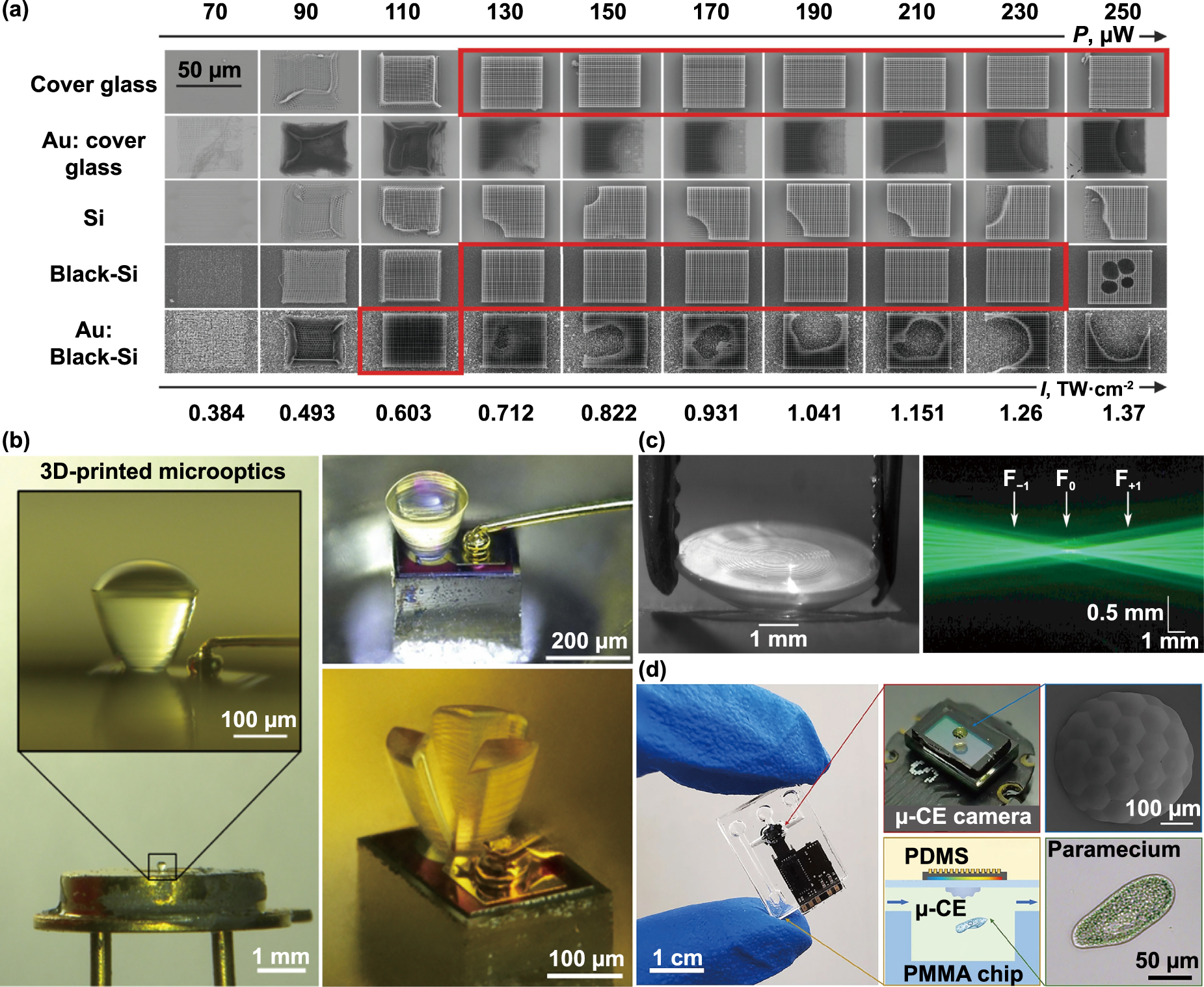
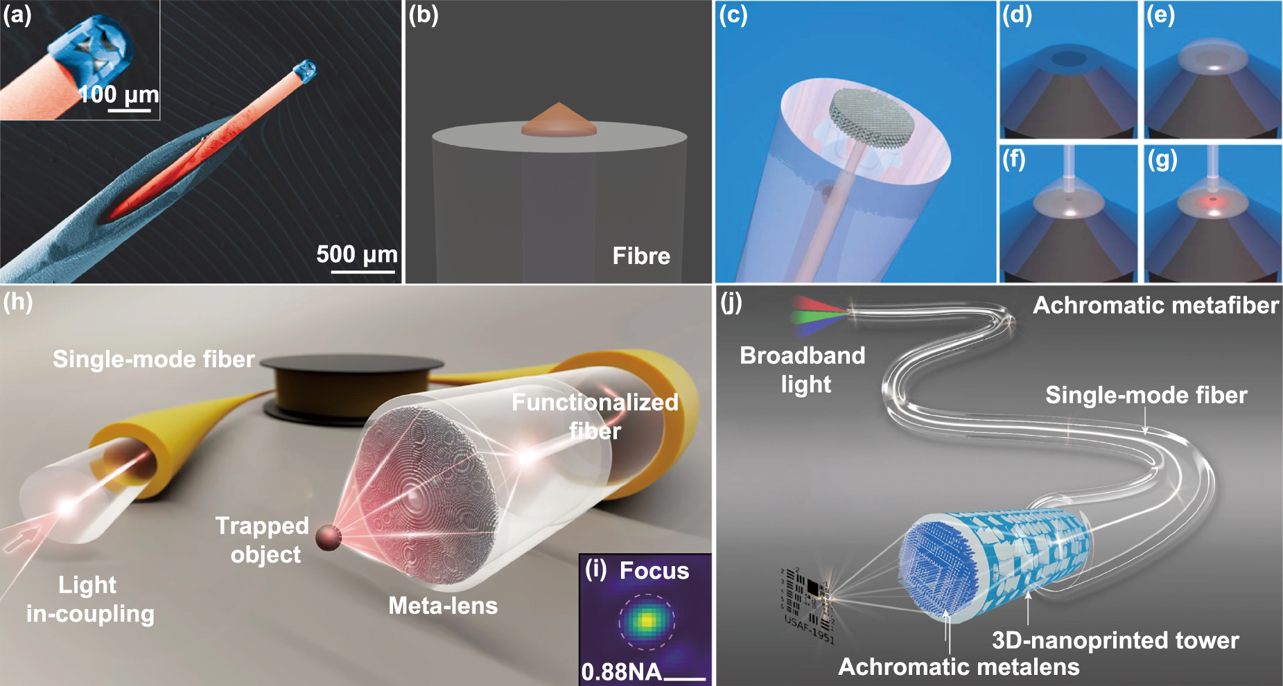
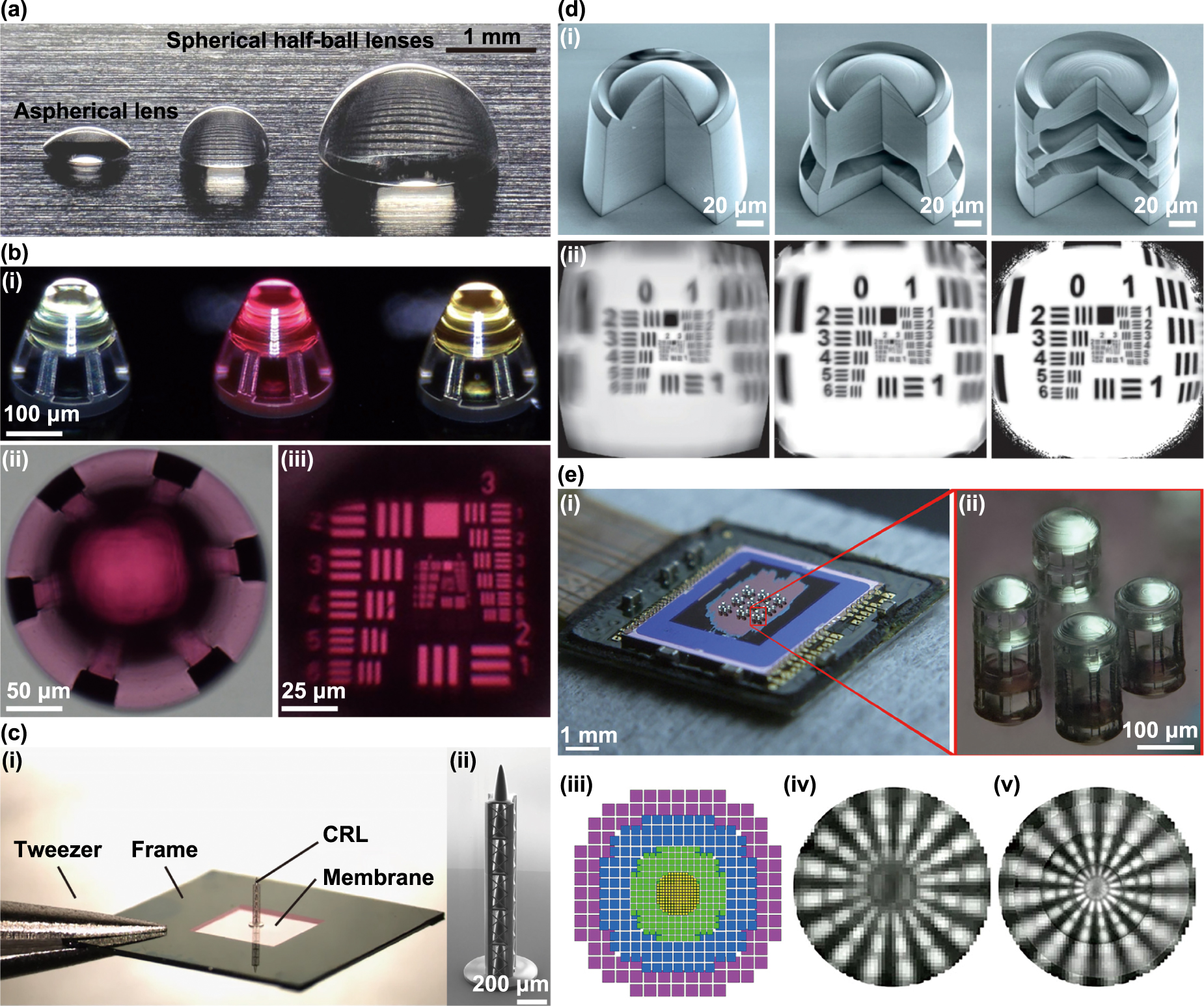
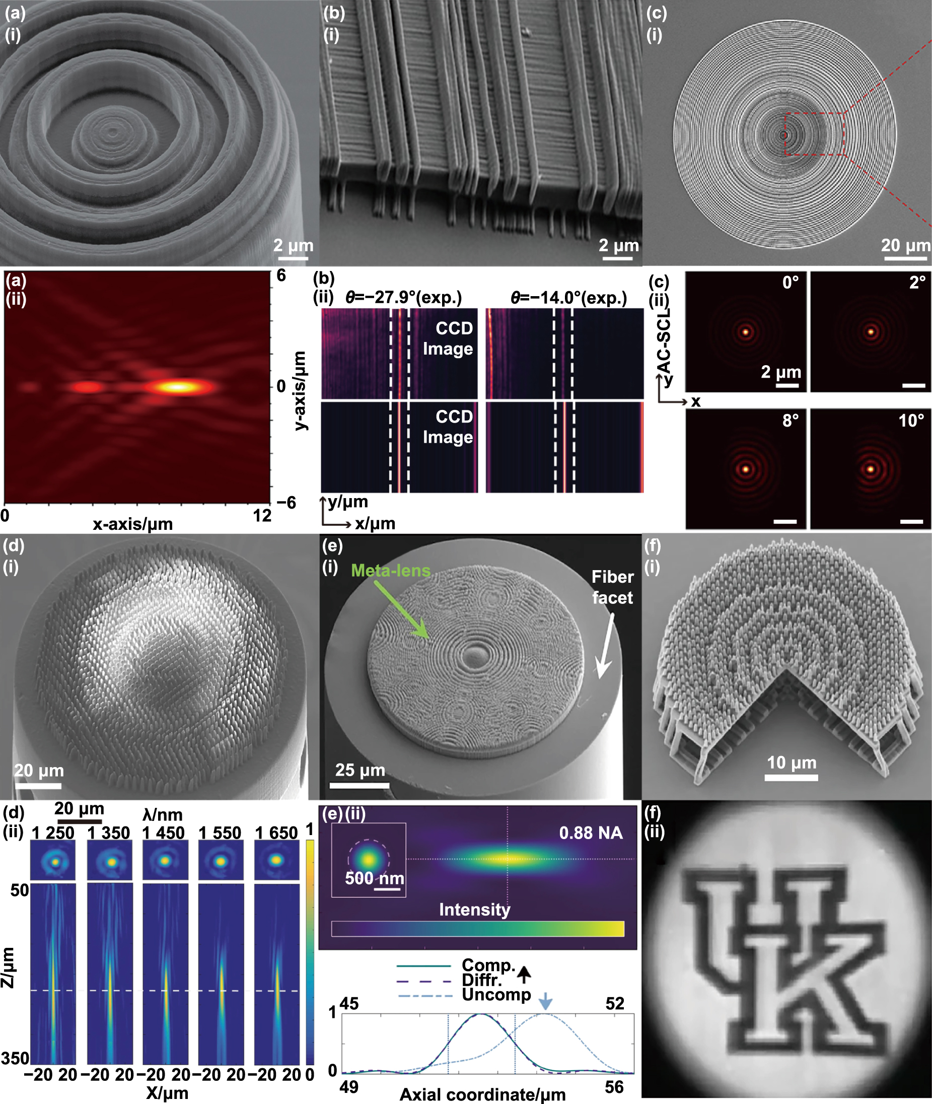
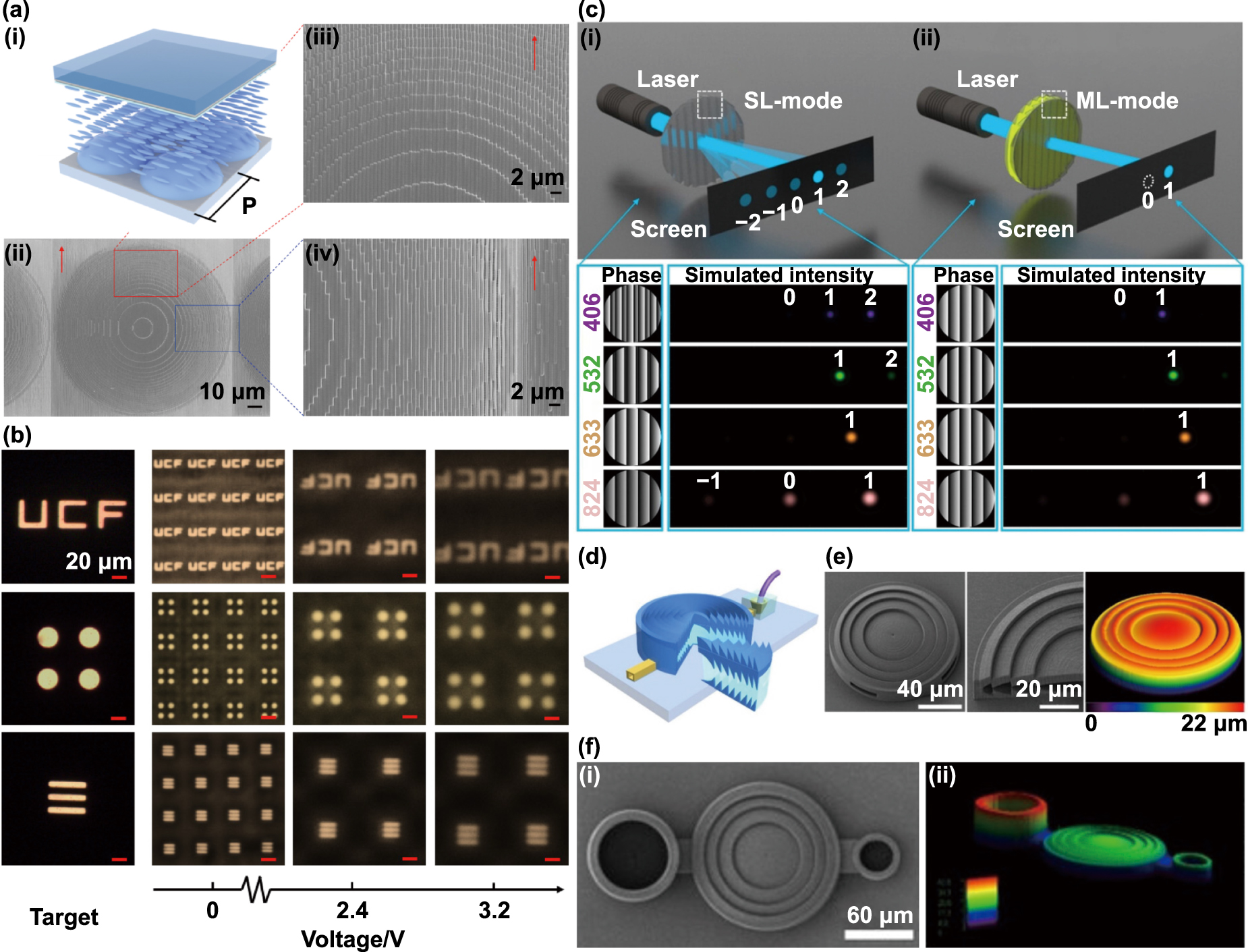
Figure 18. Schematic of the challenges and future directions of TPL for optical imaging applications.
Download figure:
Standard image High-resolution image
Furthermore, the fabrication of desired materials for intricate 3D structures using TPL holds immense promise for enhancing imaging performance and creating complex optical systems [226–229]. For instance, the integration of metals or metal alloy mounts can facilitate the incorporation of optical elements [230], leading to improved imaging contrast and enabling mirror reflections. These functionalities have been challenging to achieve with polymers, except through total internal reflection. However, though current methods such as photochemical bonding of colloidal inorganic nanocrystals significantly expanding the materials range for femtosecond laser-based 3D printing, the intrinsic size limit of nanocrystals imposes constraints on surface roughness, limiting their suitability for super-fine optical elements at present. Additionally, the utilization of 2D materials [130], perovskite materials [225], upconversion materials, or molecular crystals can enable nonlinear optical conversion, allowing the capture of x-ray, UV, and infrared information in 3D-printed imaging systems [231]. Specific inks designed for colorful imaging and light-blocking, as well as semiconductors for optoelectronic imaging devices, represent other avenues of exploration. While TPL fabrication tools equipped with multichannel to handle different materials show promise, the development of suitable photoresists remains an ongoing challenge [227]. A systematic approach to fabricating advanced nanoscale optical imaging devices via TPL across diverse material classes is imperative, opening up new frontiers in imaging device design.
Another intriguing direction involves the fusion of smart materials with TPL 3D printing, known as 4D printing [232], which introduces the possibility of multidisciplinary imaging applications with various stimuli [233, 234]. For example, optical elements crafted from shape memory polymers can exhibit varying optical functions under different states [235], while microlenses composed of biocompatible materials, like proteins that swell and shrink with changes in pH, can dynamically shift the focal spot position [166, 236, 237]. Consequently, the development of resins tailored for 4D printing will enable 3D-printed imaging elements to undergo transformations in shape and properties in response to various stimuli and precise manipulation over time. To fully unlock the potential of 4D printing in imaging optics, optimization of material selection, design, and stimulus parameters is essential. This will empower TPL-fabricated structures with unique capabilities, paving the way for innovations in soft robotics, biomimetics, biomedical devices, and sensors.
To realize the desired imaging functionality with suitable materials for optical elements, precise fabrication and characterization play pivotal roles [238]. Typically, geometric artifacts arise from the voxelization of the 3D model, translation into slicing and hatching lines, suboptimal printing parameters [239], and post-processing deformations, such as shrinkage due to incomplete polymerization and changes induced by soaking liquid evaporation. Simple artifacts with clear functional dependencies on system parameters can be readily compensated using offset algorithms by evaluating these parameters. However, addressing more complex deviations necessitates innovative strategies, such as information-based inverse design, utilizing observed geometrical changes and underlying theories. In addition, surface roughness significantly impacts the imaging quality of printed optical elements. Despite various methods introduced to reduce surface roughness, the current state-of-the-art value hovers around 5 nm. While this suffices for many miniaturized imaging devices, it falls short of the stringent requirements for high-end imaging products with surface roughness below 1 nm. Further investigation into post-processing techniques like reflow and layer deposition is essential to achieve roughness suppression to reduce the scattering and reflection loss [240].
Precise characterization of fabricated structures is crucial for geometric optimization. Conventional ex-situ methods include optical characterization, SEM, and atomic force microscopy (AFM) post-printing. However, in-situ imaging can simplify optimization by providing information about device morphology and properties before development, allowing real-time compensation during printing. Ideally, in-situ methods should offer real-time monitoring, high diffraction-limited resolution, and avoid undesirable modifications to printed devices during inspection. Currently, quantitative phase imaging (QPI) methods like OCT and optical diffraction tomography are the primary in-situ diagnostics [241]. QPI eliminates the need for complex sample preparation and provides quantitative information on reproduction fidelity, fabrication quality, surface roughness, and relative shrinkage. The examination process can be expedited further with parallel computing or machine learning algorithms. However, some considerations remain, including the need for perfect alignment for optimal resolution and the diffraction-limited spatial resolution, making it less suitable for submicron features. Additionally, artifacts may arise due to factors like focal spot formation and oligomer blob flow, complicating phase reconstruction and potentially misleading compensation and quality evaluation [242]. Furthermore, the hardware integration for diagnostics should be straightforward, and software with rapid reconstruction algorithms is required for real-time inspection [243].
High precision optical elements significantly enhance the imaging quality. For obtaining fine feature size and high printing resolution, two-beam lithography, utilizing a doughnut-shaped inhibition beam to restrain photopolymerization triggered by the writing beam at the doughnut ring, has been proposed and achieved remarkable outcomes, including a reduced feature size down to sub-10 nm and improved resolution of ∼50 nm [244]. This technique excels in fine structure fabrication, such as high-resolution metalenses and gradient lenses with locally changed refractive indices. However, its speed is naturally slow, necessitating faster scanning or multibeam approaches for large-scale fabrication. Therefore, to transition from laboratory research to industrial applications, mass production becomes imperative, which can be achieved through the development of extreme sensitive photoresists [245, 246] and high-speed TPL technologies [247, 248]. Various scanning schemes, including single beam writing with stage scanning, galvanometer scanning, rotating mirror scanning, or acousto-optic deflector (AOD) scanning, have been explored to increase speed. Stage scanning is the most widely used fabrication method with the advantage of achieving high writing speeds up to meters per second and supporting large-area structure writing with sub-hundred nanometer accuracy. However, it faces a trade-off between speed and accuracy, leading to a significant decline in accuracy at higher speeds. Issues such as acceleration-related challenges and material detachment in certain cases also pose limitations. Mirror-based scanning, whether analog or digital, provides high-speed scanning in the kilohertz range with micro-radian accuracy. Digital mirrors offer superior precision and stability, but drawbacks include difficulties in improving scanning speed and stability. Circular field limitations of objective lens also impact effective system utilization. The rotating mirror method enhances laser direct writing speed, surpassing stage scanning accuracy. It eliminates acceleration and deceleration issues, providing higher speed stability and a longer effective travel distance. However, operational noise may decrease system stability, and its scanning method may not be the most efficient for scenarios with few structures and large dimensions. AOD allows rapid laser scanning through diffraction, exhibiting features like no mechanical inertia and quick random scanning. Despite achieving scanning frequencies exceeding 250 kHz, its application in TPL systems introduces angular dispersion, reducing accuracy and uniformity. Pre-compensation strategies and reverse dispersion are required to address these issues. Energy transmittance considerations and limited scanning angles also require careful evaluation for practical applications. Since the speed is still limited by the mechanical devices, recent investigations have focused on multi-focal parallel fabrication with assistance from diffractive optical elements, interference MLAs, spatial light modulators, digital micromirror devices, light field exposure, and volume exposure [249–252]. In addition, developing technologies with continuous laser based TPL will greatly reduce the cost and expedite the scalable industrial production with high laser power and parallel processing [222, 224]. Combining these techniques with other fabrication methods for different scales can further expedite the process. Additionally, high-quality fabrication on diverse substrates, including hard brittle materials, soft flexible ones, and non-flat surfaces, remains a challenge [253]. With ongoing progress and increasing demand for high-quality imaging elements, TPL is poised to continue its development, achieving superior printing accuracy while maintaining high quality and efficiency.
With its exceptional capability to fabricate arbitrary geometries, TPL offers opportunities to realize imaging functions with unconventional optical elements beyond traditional lenses [254–256]. Furthermore, its ability to create 2D, 2.5D, and 3D structures in a single step allows for the implementation of functions superior to conventional 2D-limited metalenses [257]. TPL also extends beyond simple imaging, enabling applications such as polarization imaging, computational imaging, and imaging classification and recognition using neural networks. These designs and applications have only recently begun to emerge, necessitating rapid design methods like inverse design and fast simulation techniques capable of handling structures spanning nanometers to centimeters. In addition to imaging functions, TPL can be utilized for fabricating other imaging-related elements, including photon-collecting antenna [258], freeform lenses for imaging correction [259], custom-made phantoms with internal structures that mimic optical and structural properties of cells [260–262], and robust evaluation tools for tomographic phase microscopy [263]. It can also capture the scattering characteristics of real-world objects for optical neural network training.
Overall, TPL has significantly expanded design possibilities with its capacity to create arbitrary 3D structures. The unique ability to achieve complex optical imaging systems with self-alignment in one-step manufacturing while maintaining nanoscale precision makes it outperform other technologies with special convenience for global optimization design and fast integration. Coupled with the rapid advancements in materials and fabrication techniques, TPL is ready to replace traditional fabrication methods in specific imaging applications and explore new directions and fields for imaging with compact configurations and outstanding optical performance [169, 183, 264–268]. We envision that the future development will promise to reduce the cost significantly, facilitating the transition of this technology from the laboratory to industry for the mass production of more reliable and complex imaging systems and applications.
Acknowledgments
H W and J K W Y acknowledge the support from the National Research Foundation (NRF) Singapore, under its Competitive Research Programme Award NRF-CRP20-2017-0004 and NRF Investigatorship Award NRF-NRFI06-2020-0005, the MTC Programmatic Grant M21J9b0085, as well as the Lite-On Project RS-INDUS-00090. H R acknowledges the support from Australian Research Council (DE220101085, DP220102152). M A S acknowledges the grants from German Research Foundation (SCHM2655/15-1, SCHM2655/21-1). S A M acknowledges the Lee-Lucas Chair in Physics and funding by the Australian Research Council DP220102152. Y H and H D thanks the financial support from the National Natural Science Foundation of China (Grant No. 62275078), Natural Science Foundation of Hunan Province of China (Grant No. 2022JJ20020) and Shenzhen Science and Technology Program (Grant No. JCYJ20220530160405013).