

Abstract
The ever-increasing demand for energy as a result of the growing interest in applications, such as the Internet of Things and wearable systems, etc, calls for the development of self-sustained energy harvesting solutions. In this regard, 2D materials have sparked enormous interest recently, due to their outstanding properties, such as ultra-thin geometry, high electromechanical coupling, large surface area to volume ratio, tunable band gap, transparency and flexibility. This has given rise to noteworthy advancements in energy harvesters such as triboelectric nanogenerators (TENGs), piezoelectric nanogenerators (PENGs) and photovoltaics based on 2D materials. This review introduces the properties of different 2D materials including graphene, transition metal dichalcogenides, MXenes, black phosphorus, hexagonal boron nitride, metal-organic frameworks and covalent-organic frameworks. A detailed discussion of recent developments in 2D materials-based PENG, TENG and photovoltaic devices is included. The review also considers the performance enhancement mechanism and importance of 2D materials in energy harvesting. Finally, the challenges and future perspectives are laid out to present future research directions for the further development and extension of 2D materials-based energy harvesters.
Export citation and abstract BibTeX RIS

Original content from this work may be used under the terms of the Creative Commons Attribution 4.0 license. Any further distribution of this work must maintain attribution to the author(s) and the title of the work, journal citation and DOI.
1. Introduction
The growing demand for flexible, portable, and wearable electronics has led to significant research in the development of a sustainable and easily integrable power source [1–3]. Li-ion batteries are currently dominating the market for portable power sources. Batteries are not the right choice since they are not sustainable and have a significant negative impact on the environment. Moreover, batteries require frequent replacement, and the recycling of Li-ion batteries is a major challenge [4, 5]. On the other hand, the conversion of mechanical and solar energy to electricity offers a promising solution for driving wearable electronics and self-powered sensors [6–13]. With regard to mechanical energy, low-frequency energy harvesters, such as piezoelectric nanogenerators (PENGs) and triboelectric nanogenerators (TENGs) offer unique advantages, such as being lightweight, portable and flexible [1, 12, 14]. The first PENG-based ZnO nanowire was reported in 2006, while TENG was developed recently, in 2012 [8, 15]. The relatively high output and wide choice of materials and device design are some of the distinctive features of TENGs [16–18]. However, PENGs are more stable compared to TENGs. These nanogenerators can also be introduced into textiles to allow integration with everyday clothing.
The nanogenerators have been successfully demonstrated to harvest wind energy, water-wave energy, cell stimulation, physical, chemical and biosensors, drug delivery, wound healing, microbial disinfection, gene delivery, etc [19–23]. Compared to these nanogenerators, photovoltaics (PVs) generate high electrical current [24, 25]. Earth receives an abundance amount of solar energy, which is one of the best carbon neutral green sources. Si and thin-film-based PVs are continuously evolving semiconducting technologies that convert sunlight into electricity with the current state of the commercial panel enabling power conversion efficiency (PCE) close to ∼25% [26]. The current global solar PV power generation capacity is around 400 GW, which is expected to reach 4.7 TW by 2050 [27]. This high demand comes with the benefitof reducing the cost of the PV module and the possibility to optimize the maximum power per unit mass of the cells. Bulk semiconductor-based junction PV cells follow the standard manufacturing where the cost reduction reaches a saturation $2/W, which poses significant challenges for further reduction. In this regard, the third generation solar cells, such as those based on organics and perovskites, show significant promise, as they produce power on par with Si-based PVs with additional merits, such as low cost, flexibility and stability [28, 29]. The incorporation of 2D materials, such as graphene, transition metal dichalcogenides (TMDs), black phosphorus (BP), etc, could further enhance their PCE beyond 20% and improve their usage for renewable energy generation [30, 31]. The merits of using 2D materials in PV architectures are improved cell performance due to superior electrical properties (high mobility, band gap, optical absorption and transparency), scalability, low-cost manufacturing and material stability.
The substantial advances in nanotechnology and manufacturing processes have led to innovations in the materials, device fabrication and printed electronics approaches for improving the performance of electronic devices including energy harvesters [32–35]. In 2004, graphene was exfoliated from graphite and since then, 2D materials have attracted tremendous attention from the wider scientific community for numerous applications including nanogenerators, electromagnetic shielding, flexible electronics, nanoelectromechanical systems and sensors [36–47]. The extensive interest in 2D materials lies in their high surface area, transparency and excellent electronic and mechanical properties [48]. Quantum confinement in 2D materials results in intriguing charge transport and band structures, endowing the 2D materials with alluring optoelectronic and electrical performance [48, 49]. Tuning the chemistry and structure of 2D materials allows easy control over their properties to impart high performance to the device. The family of 2D materials includes TMDs, graphene, graphene oxide (GO), BP, metal- or covalent-organic frameworks (MOFs/COFs), MXenes and hexagonal boron nitride (h-BN) (figure 1) [48, 50–53]. For TENGs, 2D materials can serve as electrodes, active triboelectric layers or both.
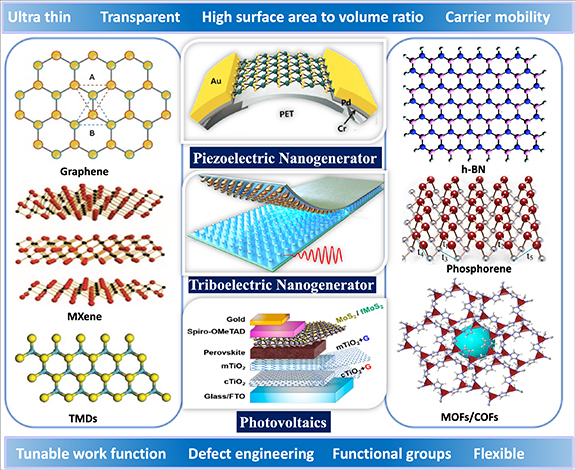
Figure 1. Structure of 2D materials and their properties for energy harvesting via PENGs, TENGs and PVs. Graphene: Reprinted from [69], Copyright (2010), with permission from Elsevier. MXene: Reproduced from [50]. CC BY 4.0. TMDs: Reprinted from [51], Copyright (2018), with permission from Elsevier. Piezoelectric nanogenerator: [70] John Wiley & Sons. © 2018 WILEY-VCH Verlag GmbH & Co. KGaA, Weinheim. Triboelectric nanogenerator: Reproduced from [23]. CC BY 4.0. © 2022 The Authors. Advanced Materials published by Wiley-VCH GmbH. Photovoltaics: Reprinted with permission from [30] Copyright (2019) American Chemical Society. h-BN: Reproduced with permission from [52]. CC BY-NC 4.0. Phosphorene: Reprinted figure with permission from [71], Copyright (2021) by the American Physical Society. MOFs/COFs: [53] John Wiley & Sons. © 2019 WILEY-VCH Verlag GmbH & Co. KGaA, Weinheim.
Download figure:
Standard image High-resolution imageThis review article focuses on the 2D materials for TENGs, PENGs and PVs. Section 2 briefly discusses the characteristics of different 2D materials used for energy harvesting. Section 3 covers the mechanism of PENG, the prime requisite factors for materials to exhibit piezoelectricity, and the influence of monolayers and bilayers in structured devices for piezoelectric energy harvesting. In addition, strategies for incorporating 2D materials as fillers for enhancing the output performance of PENGs are highlighted. Section 4 introduces the basic mechanism and device modes of TENG along with the role of 2D materials as electrodes, active triboelectric layers and dual roles, i.e. active triboelectric layers as well as electrodes. The details of the underlying mechanism for the enhancement in performance are discussed. Section 5 details the importance of 2D materials for bulk, organic and perovskite-based PVs. Finally, section 6 discusses the challenges and future perspectives of the field.
2. 2D materials
The properties of monolayer and few-layer 2D materials differ greatly from their bulk counterparts, thus exhibiting the quantum spin Hall effect and Dirac fermion quantum phenomenon [54–58]. The 2D materials are stacked with weak van der Waals (vdW) interactions [56, 57]. This section emphasizes the properties of 2D materials relevant to energy harvesting.
2.1. Graphene family
Graphene is a 2D structure comprising hexagonally arranged sp2-hybridized carbon atoms. The attractive properties of graphene include high electron mobility (200 000 cm2V−1S−1), electrical conductivity (2000 S m−1), specific surface area (2630 m2g−1), high mechanical strength (Young's modulus 1 TPa) and excellent optical transparency (∼97.7%) [59–63]. High conductivity is an essential requirement for electrode materials. GO, few-layer graphene, reduced GO (rGO) and graphene nanosheets are members of the graphene family. The conductivity of GO is poor compared to graphene due to the presence of oxygenated functional groups [64]. GO is more suitable as a triboelectric material than as an electrode due to its high surface area and ability to gain electrons in frictional contact.
2.2. Transition metal dichalcogenides (TMDs)
TMDs are MX2-type semiconductors, where M is the transition metal (W, Mo) and X is the chalcogen (Te, Se or S). The 2D TMDs include MoS2, MoSe2, WS2 and WSe2 [65]. TMDs have garnered tremendous attention in applications, such as energy harvesting, spintronics and optoelectronics, due to their direct band gap, atomic level thickness and quantum confinement [65, 66]. MoS2 is the most widely studied member of the TMD family and exists in 1H and 2H (hexagonal), 1T (trigonal) and 3R (rhombohedral) phases [65]. MoS2 was used as a charge trapping material and is known to suppress charge recombination to enhance the TENG output [67]. The 1T metallic MoS2 exhibits high electrical conductivity, making it suitable as an electrode material in TENGs [68].
2.3. MXenes
MXenes are an emerging class of 2D materials, comprising transition metal carbides, carbonitrides and nitrides. Typically, MXenes are Mn +1Xn Tx where M is the transition metal (Ti, Zr, V), X is the carbon or nitrogen, T is the surface functional group (–F, –O and –OH) and n ranges from 1–3 leading to M2XTx , M3X2Tx and M4X3Tx structures [72, 73]. MXenes are mainly synthesized by etching of the A element from MAX phase (Mn +1AXn ), where A is a group IIIA or IVA member [72, 73]. The interesting properties of MXenes include excellent electrical conductivity and mechanical properties, a functionalized surface, and high stability of the colloidal solution [73]. Thus, MXenes can act as an electrode in energy harvesting devices. In addition, the abundance of surface functional groups provides MXenes with more tribonegative characteristics than Teflon [74, 75].
2.4. Hexagonal boron nitride (h-BN)
The hexagonal structure of h-BN comprises an equal number of boron and nitrogen atoms, endowing unique properties to h-BN including low dielectric constant, chemical inertness and excellent thermal conductivity [76]. The electrical properties of h-BN can be tuned by doping, defect engineering and functionalization. The h-BN was hybridized with MoS2 to improve the performance of TENG by enhancing the electron acceptance capabilities [77].
2.5. Black phosphorus (BP)
BP is a layered material, with a modest band gap exhibiting semiconductor properties. Phosphorene is a monolayer BP with an orthorhombic crystal structure. The attractive properties of phosphorene include high carrier mobility, optical transparency, ductility along the in-plane direction, and tunable band gap [78]. However, phosphorene is unstable under ambient conditions due to its high reactivity with oxygen [79]. To improve the stability, several attempts have been made, including hybridization with other materials, surface functionalization, encapsulation, liquid-phase surface passivation and doping [80, 81]. BP was used as an electron-trapping layer to enhance the performance of TENG [80].
2.6. Metal-organic frameworks (MOFs) and covalent-organic frameworks (COFs)
MOFs are porous materials where metal ions are connected by a strong bond to an organic ligand or linker. Since their discovery in 1990, MOF research has witnessed enormous growth, particularly in the past two decades. Over 90 000 MOFs have been developed already, and nearly 500 000 MOF structures were predicted [82]. The wide availability of metal ions and organic ligands gives rise to the development of thousands of different MOFs [83]. MOFs obey isoreticular principle, i.e. different organic ligands with common geometry or symmetry can be used to produce MOFs with similar topology and may have different pore size or pore volume [83]. MOFs have been explored for a wide range of applications including energy harvesting, energy storage, catalysis, sensing and gas separation [53, 84–86]. The wide range of MOF applicability is attributed to its high surface area to volume ratio, ease of post-synthetic modifications, tunable porosity and ease of functionalization. COFs are also porous materials, but they consist of light elements, such as carbon, hydrogen, nitrogen, boron, etc. The COFs are lighter than MOFs while maintaining excellent stability and porosity. Similar to MOFs, COFs can be easily modified and functionalized [87]. The high surface area of MOFs/COFs makes them suitable as TENG active triboelectric layers. The specific pore size of MOFs/COFs is advantageous to achieving high sensitivity and selectivity for self-powered sensing [53]. Furthermore, MOFs can also be used to fabricate humidity-resistant TENG devices [88]. In PENGs, MOFs can be used to improve the electroactive phase and can lead to high piezoelectric coefficients [89].
3. Piezoelectric nanogenerator
The phenomenon of piezoelectricity was first discovered in 1880 by Pierre Curie and Jacques Curie while working on the crystals of quartz and Rochelle salt [90]. The piezoelectric effect refers to the coupling phenomenon of mechanical stress and electric charge separation. It is the ability of materials with non-centrosymmetric crystal structures to generate electric polarization in response to applied mechanical stress. This is denoted as the direct piezoelectric effect and forms the basis for versatile applications in energy harvesting and sensing systems [91–95]. As the piezoelectric effect is reversible, materials that exhibit direct piezoelectric effect also display converse piezoelectric effect, implying the induction of mechanical strain in response to an applied electric field. The inverse piezoelectric effect has been extensively employed in the construction of actuators, motors and acoustic emitters [96].
Although the appearance of piezoelectricity dates back to 1880, it was only in 2006 when the PENG term was coined [8]. Since its inception, PENGs have unveiled a promising approach to harvesting locally accessible mechanical energy and converting it into usable electrical energy based on the piezoelectric effect. Figure 2(a) depicts the basic working mechanism of a PENG device. When a PENG device is subjected to an external force, the embedded crystal structure experiences deformation, as a result of which charge separation occurs, leading to the creation of potential differences across the material. To counter this piezoelectric potential, positive and negative charges are accumulated on the electrodes, resulting in a one-half cycle of the AC output. Upon withdrawal of the force, the generated potential difference across the electrode declines resulting in the accumulated charges being transposed back in the opposite direction, thereby providing the other half of the PENG AC output [97]. Accordingly, continuous signals from the device can be acquired by subjecting it to periodic compression and release cycles of force.

Figure 2. (a) Working mechanism of a piezoelectric nanogenerator device. Reprinted from [106], Copyright (2019), with permission from Elsevier. (b) Predicted piezoelectric charge coefficients of 2D materials [104, 106, 107].
Download figure:
Standard image High-resolution imageIn general, the piezoelectric energy harvesting performance is significantly influenced by the direction of applied stress. This mainly comprises two modes of operation. When the direction of applied stress and the voltage generation occur along the same direction, the device is said to be working in d33 mode. While if the stress applied is perpendicular to the direction of voltage generation, the device is said to be functioning in d31 mode. The performance of PENG is thereby computed directly by the magnitude of the piezoelectric charge coefficient, dij, where i represents the direction of polarization and j refers to the direction of applied stress [91].
Accompanying the discovery of piezoelectricity in quartz, a substantial number of material classes encompassing various chemical compositions and crystal structures were shown to exhibit intriguing piezoelectric responses. Traditional 3D piezoelectric materials, such as PZT (lead zirconate titanate) and BTO (barium titanate), are restricted to practical applications despite their exhibiting excellent piezoelectric characteristics due to their brittle nature and severe toxicity arising from lead in the case of PZT [98]. Moreover, the ever-expanding demand for miniaturization calls for low-dimensional materials combined with superior piezoelectric properties. Although 1D ZnO nanowires exhibit a fairly good piezoelectric response, their poor compatibility with the manufacturing process raises considerable concerns [99, 100]. In this regard, 2D materials are exceedingly becoming a class of burgeoning interest because of their ultra-thin geometry, flexibility, excellent electromechanical response, transparency and atomic layer thickness, thus providing endless opportunities for their use in multifunctional applications [101]. While the presence of a band gap and a non-centrosymmetric crystal structure is indispensable for a material to exhibit intrinsic piezoelectricity, surface engineering can be leveraged as an effective strategy to introduce asymmetricity and thereby piezoelectricity [102]. One such example is graphene, which in its pristine state is non-piezoelectric due to its intrinsically centrosymmetric structure, but by adsorption of foreign atom inversion symmetry can be broken and piezoelectricity can be effectively induced [103]. The 2D materials are broadly classified into three groups: III–V materials, metal dichalcogenides and monochalcogenides based on their in-plane structure. Figure 2(b) depicts various classes of 2D materials along with their piezoelectric coefficients [104, 105].
For the very first time, piezoelectric properties in 2D materials were investigated through theoretical calculations closely followed by an experimental demonstration [104, 107]. The piezoelectricity of single atomic layer 2D MoS2 was validated and demonstrated for mechanical energy harvesting [108]. The MoS2 flakes were exfoliated by mechanical means, the thickness of which was precisely measured by atomic force microscopy and confirmed by Raman spectroscopy. The crystallographic orientation of these flakes was derived from SHG experiments. Finally, a flexible device comprising a single-layer MoS2 flake was fabricated by transferring flakes to a polyethylene terephthalate (PET) substrate followed by Cr/Pd/Au (1 nm/20 nm/50 nm) electrode deposition. It was observed that under a strain of 0.53% along the armchair configuration, a maximum output voltage of 15 mV and a current of 20 pA could be generated. Consequently, a power density of 2 mW m−2 was achieved with ∼5.08% mechanical to electrical energy conversion efficiency. However, applying strain in a zigzag direction leads to diminished output signals. In addition, the piezoelectric response from an increased number of atomic layers (n = 2, 3, 4, 5, 6) in MoS2 flake and the bulk MoS2 sample was assessed. Interestingly, only layers with odd numbers displayed piezoelectric output, while no signals were detected with an even number of layers and the bulk sample. The output response displays a decreasing trend on increasing the layer thickness. These outcomes reveal that monolayer MoS2 possesses inherent piezoelectricity on account of its broken inversion symmetry, whilst bilayers and bulk crystals are non-piezoelectric due to the development of centrosymmetric structures.
Inspired by this work, the exploration of piezoelectric properties of various 2D materials started gaining enormous momentum. In a successive study, a 2D monolayer MoS2 grown by chemical vapor deposition (CVD) was employed for flexible PENG, and an in-depth analysis of direction-dependent piezoelectric effects was examined [109]. Depending upon the geometric orientation of MoS2, it can exhibit either armchair or zigzag configuration, which is bound to significantly influence the magnitude of piezoelectric coefficients. Hence, lateral piezoresponse force microscopy (PFM) analysis was conducted to determine their piezoelectric response. From the measured response, as can be seen from figure 3, d11 of 3.78 pmV−1 was obtained in the armchair configuration, while the measurement along the zigzag direction resulted in a much lower value of d11= 1.38 pmV−1, signifying the existence of anisotropic piezoelectric properties in MoS2. Based on these outcomes, a monolayer MoS2 PENG was fabricated. Almost twice the output voltage (20 mV) was achieved with the device composed of the armchair direction of MoS2 rather than the PENG with zigzag direction (10 mV) under the same bending strain of 0.48%, indicating directionality being a crucial factor in enhancing the output performance of MoS2 monolayer PENGs.
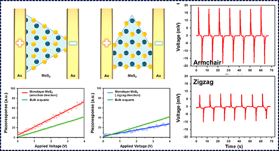
Figure 3. Schematic diagram depicting the lateral PFM measurement setup and the corresponding piezoresponse in armchair configuration and in the zigzag direction of MoS2. Reprinted from [109], Copyright (2016), with permission from Elsevier.
Download figure:
Standard image High-resolution imageAlthough CVD is one of the most widely used techniques for the synthesis of 2D materials, it unavoidably results in the formation of defects. These defects introduce free electrons, which in turn produce a potential screening effect that diminishes some of the piezoelectric potential developed under mechanical deformation and thereby reduces the piezoelectric effect. For instance, S vacancy in MoS2 acts as an n-type carrier in MoS2 and generates a screening effect. Therefore, the n-type carrier density should be decreased in order to enhance the piezoelectric properties of MoS2. In an exciting study, a CVD-grown MoS2 PENG was described via S vacancy passivation and the results before and after S treatment were analyzed [70]. It was found that the S-treated monolayer MoS2 nanosheet-based PENG exhibited an increase in current of more than three times (100 pA) along with a twofold increase in voltage (22 mV) in comparison to the pristine MoS2 PENG (figure 4(a)). Furthermore, an impressive tenfold enhancement in the output power was obtained (73 µW m−2). These findings elucidate that S treatment helps reduce the electron concentration on the pristine MoS2 surface and effectively prevents the screening effect, which is critical for enhancing the output performance of the PENG.
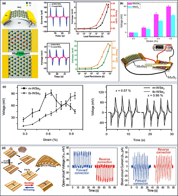
Figure 4. (a) Schematic illustration of MoS2 nanosheet-based PENG and depiction of S vacancy before and after treatment. Output performance and load matching analysis of pristine and S-treated MoS2 PENG. [70]. John Wiley & Sons. © 2018 WILEY-VCH Verlag GmbH & Co. KGaA, Weinheim. (b) Output comparison of MoS2 and MoSe2-based PENG devices and its demonstration to drive a MoS2 pH sensor. Reprinted with permission from [110]. Copyright (2020) American Chemical Society. (c) Peak output voltages derived from monolayer and bilayer WSe2 with respect to strain%, and at 0.57 and 0.95% strain. [111] John Wiley & Sons. © 2017 WILEY-VCH Verlag GmbH & Co. KGaA, Weinheim. (d) Diagram illustrating the transfer process of h-BN NF. Open-circuit voltage (OCV) and short-circuit current derived from single h-BN NF in forward and reverse connections. Reprinted with permission from [112]. Copyright (2019) American Chemical Society.
Download figure:
Standard image High-resolution imageIn addition to MoS2, other 2D TMDs, such as MoSe2, MoTe2, WS2 and WSe2 have also been found to exhibit intriguing piezoelectric properties. The piezoresponse exhibited by monolayer MoSe2 (60 mV at 0.6% strain) was almost 50% larger than that of MoS2 (figure 4(b)) [110]. A flexible PENG fabricated with monolayer MoSe2, which was derived from CVD, demonstrated noteworthy electromechanical energy conversion (∼7.2%), which was seen to successfully drive a pH sensor and a photodetector based on MoS2 and MoS2/WSe2 heterojunction, respectively.
Whilst monolayer TMD materials exhibit peculiar piezoelectricity, nearly compared to the existing traditional piezoelectric materials, their mechanical endurance for practical implementation raises serious concerns. Multi-layered structures present one of the crucial ways to address this issue. However, in general, TMDs in multi-layered configurations display considerably eliminated piezoelectricity due to the presence of an inversion center due to the alternating polarization directions in the structure. In 2012, the occurrence of reliable piezoelectricity was demonstrated in WSe2 bilayers by adopting a layer-by-layer stacking approach (turbostratic stacking) [111]. In contrast to the monolayer WSe2 fabricated nanogenerator in which the device performance started to show a significant decline over strain of 0.63%, the bilayered WSe2 device was seen to withstand strains of up to 0.95% while retaining an output voltage of 85 mV (figure 4(c)). The emergence of prominent mechanical properties in bilayer WSe2 stems from the high Young's modulus along with the interlayer sliding phenomenon existing in bilayer TMDs.
In addition to TMDs, piezoelectricity in 2D h-BN nanoflakes was realized in an analysis conducted in 2019 [112]. By envisaging mechanochemical exfoliation, a 2D h-BN nanoflake was obtained with an average lateral size of ∼0.82 µm and a thickness of ∼25 nm. It was subsequently transferred onto an electrode line-patterned flexible substrate to examine its energy conversion efficiency (figure 4(d)). Upon mechanical agitation, an alternating piezoelectric output voltage of 50 mV and a current of 30 pA could be generated. Correspondingly, the piezoelectric voltage coefficient (g11) of 2.35 × 10⁻³ Vm N−1 was determined.
Considering the difficulties associated with monolayer BP fabricated devices that undergo rapid oxidation in air, it was later that the piezoelectricity in multilayer BP was delineated. Due to the spring-shaped structure of BP, the loss of piezoelectricity in multilayer BP is constrained, unlike the case with other 2D materials [113]. In this work, the authors described the energy harvesting properties of multi-layered BP along the armchair orientation by exfoliating Te-doped BP flakes onto a PET substrate. The constructed devices revealed an output current of 4 pA on subjection of a compressive strain of −0.72%, providing opportunities to design biomedical harvesting devices (figure 5(a)).

Figure 5. (a) Spring-shaped structure of BP, an optical image of the as-fabricated multilayer BP PENG device along the armchair orientation and its output current in the forward and reverse directions. [113]. John Wiley & Sons. © 2020 WILEY-VCH Verlag GmbH & Co. KGaA, Weinheim. (b) Schematic showing the formulation of MoS2-PVDF composite NFs. Output response of leaf and matchstick when fallen from different heights at the surface of a PENG device. Output voltage response and capacitor charging capabilities of PENG. [121] John Wiley & Sons. © 2017 Wiley-VCH Verlag GmbH & Co. KGaA, Weinheim.
Download figure:
Standard image High-resolution imageIn 2012, piezoelectricity in 2D SnSe crystals was demonstrated for the first time [114]. SnSe flakes obtained using a mechanical exfoliation process were seen to generate an output voltage of 760 mV. Consequently, a maximum power density of 28 mW m−2 was attained resulting in an energy conversion efficiency of 6.5%. Moreover, SnSe displayed anisotropic piezoelectric characteristics, wherein the piezoresponse along the armchair configuration was almost five times larger than that along the zigzag orientation. Nanogenerators constructed using SnSe materials were also able to monitor human activity, including vital health parameters, such as heart and pulse rate. In addition, the authors demonstrated a self-powered sensor unit solely realized using 2D material. By integrating a SnSe nanogenerator and a MoS2 sensor on one chip, an all-in-one system was tested and seen to reveal remarkable sensing performance.
Recent studies have shown a tremendous upsurge towards the fabrication of PENGs based on polymeric composites of 2D materials. This is due to the multiple advantages introduced by these composites, which include high mechanical robustness, ease of manufacturing, excellent chemical resistance and low cost. In this regard, PVDF and its copolymers, such as PVDF-TrFE, are very promising choices for energy harvesting due to their excellent piezoelectric and ferroelectric properties, superior thermal and chemical stability, and biocompatibility [115]. PVDF is a semi-crystalline polymer that exhibits five crystalline phases namely, α, β, γ, δ and  . In order to utilize PVDF for energy harvesting applications, nucleation of the electroactive β phase is highly desired. However, in contrast, the α phase is the most thermodynamically favored, but lacks the crucial piezoelectric attributes. Therefore, enriching the β phase by modulating the 2D material as a filler serves as an attractive approach for realizing improved performance of piezoelectric energy harvesters. The high surface-to-volume ratio furnished by 2D materials adds to the capacitance of the micro-capacitor incorporated in the material. In addition, interfacial interactions occurring between 2D materials, and the polymeric chains orient the chains in a favorable arrangement, which is required for yielding high-performing composite materials.
In 2020, piezoelectric enhancement studies were conducted by the addition of rGO into the PVDF matrix and was subsequently investigated for energy harvesting application [116]. A sonication-assisted method was adopted to prepare rGO nanosheets. The nanocomposite film of PVDF/rGO was then fabricated via a solution-casting process. The as-formulated composite film was extensively characterized by XRD, which revealed the presence of both α and β phases. However, as the concentration of rGO increased in the PVDF, the peaks associated with the β phase displayed significant enhancement that kept increasing with increased concentration of rGO. The surface morphology examined by SEM revealed random distribution of rGO nanosheets in the polymer matrix. Moreover, a quantitative analysis of β phase content was performed by envisaging FTIR experiments, which showed an increase from 53% to 70% and corroborated well with the XRD results. This signifies that the addition of rGO contributes largely towards the nucleation of β phase. In addition, the ferroelectric response of the nanocomposite displays a noteworthy improvement in remnant polarization values in comparison to pure polymer. Upon examination of the piezoelectric energy harvesting capabilities of the nanocomposite, the output voltage demonstrated an increase from 0.886 to 1.915 V, indicating an enhancement in the piezoelectric properties. In addition, the composite films demonstrated a 13.8% enhancement upon exposure to UV-vis light under identical testing conditions.
PVDF-TrFE, one of the copolymers of PVDF, is attracting widespread attention due to its relative ease of obtaining β phase, which is reasonably unaffected by the fabrication conditions [1, 117–119]. In an interesting study, rGO/PVDF-TrFE composite films were formulated by employing a scrap coating method and in situ electric polarization was accomplished to yield PENGs with enhanced performance characteristics [120]. The effect of adding rGO to PVDF-TrFE was extensively analyzed by XRD and FTIR measurements, which revealed improved crystallinity of the β phase due to the formation of hydrogen bonds between the oxygen groups in rGO and the F atoms in PVDF-TrFE chain. As a result of these interactions, facile orientation of CH2-CF2 dipoles in polymeric chains in one direction was obtained, which were further aligned by the in situ electric polarization process. The piezoelectric performance demonstrated a maximum open-circuit voltage of 8.3 V and a short-circuit current of 0.6 μA. Correspondingly, a maximum power density of 28.7 W m−3 was achieved, which was twice as high as that from a pure PVDF-TrFE-based device.
In addition to graphene derivatives, composite formulation based on other 2D materials is also actively pursued. In 2017, a 2D piezoelectric MoS2 nanogenerator and a nanosensor composed of PVDF nanofiber webs (NFWs) for self-power electronics were reported [121]. For the very first time, the authors disclosed an ultra-sensitive PENG made up of a few layers of MoS2 nanosheets contained in electrospun PVDF NFs. The PENG was seen to provide distinguished electrical output responses even when extremely light objects such as leaves and matchsticks fell from different heights (30, 25 and 20 cm) indicating precise detection of minuscule changes in mechanical impact (figure 5(b)). Such high-level detection capability opens up potential industrial applications towards counting batch products alongside quality monitoring and safety packaging. This indicates a major contribution rendered by MoS2 nanosheets in the PVDF NFWs. PVDF occupies interstitial sites in MoS2 and vice versa, wherein an interaction between the -CH2 dipoles with S atoms and CF2 dipoles with Mo takes place leading to the formation of favorable interactions desired for the nucleation of electroactive crystalline phases in the polymer. The presence of labile Mo-S bonds that undergo rapid deformation upon stress is one of the chief reasons for contributing to the ultra-sensitivity of PENG. Spurred by the promising output response of the device, the authors examined its efficacy towards speech recognition and demonstrated a 70-fold improvement in acoustic sensitivity to sensors made from neat PVDF NFW, establishing its viability in the biomedical sector. Furthermore, ultrafast charging capabilities i.e. 9 V in 44 s was exhibited by the PENG device providing possible routes to power up electronic equipment instantly.
Stimulated by the incorporation of 2D TMD materials as a filler for enhancing the overall output performance of a PENG device, a recent study reported WS2/PVDF nanocomposites and demonstrated colossal energy conversion efficiency of 25.6%, which is the highest among the values reported for PVDF-2D materials-based PENG [122]. In this work, WS2 nanosheets were chemically exfoliated and dispersed into dimethylformamide (DMF) to which PVDF powder was added forming homogeneous WS2/PVDF nanocomposites. Systematic analysis revealed no change in the optical or crystallinity of WS2 nanosheets. Finally, fabricated WS2/PVDF composed flexible devices were subjected to test under 105 kPa, which resulted in a supremely high piezoelectric output voltage of 116 V. Moreover, a piezo-phototronic device, under the illumination of 410 nm, delineated a high responsivity (6.98 × 10⁻³ A W−1) and detectivity (8.61 × 1010 cm H1/2 W−1) at a strain of 0.75%, opening up new avenues towards constructing photosensitive multifunctional PENG devices for portable electronic devices.
In addition to TMDs, the latest trend has started witnessing the usage of other classes of emerging 2D materials, namely MXene towards piezoelectric energy harvesting capabilities. In a study performed in 2021, the incorporation of MXene as the filler into PVDF-TrFE was investigated and its dependence and influence on the piezoelectric properties were examined [123]. The presence of numerous functional groups on the surface of MXene provides unique opportunities to interact with PVDF-TrFE chains together with their increased electrical conductivity, which can aid in better polarization of PVDF-TrFE, during electrospinning (figure 6). The piezoelectric fabricated devices were subsequently tested under a force of 20 N and a frequency of 1 Hz. A maximum output voltage of 1.5 V was obtained for the optimized 2 wt% MXene composite device, which was almost three times higher than that obtained from the pure polymeric device. Apart from displaying superior energy harvesting capabilities, MXenes also provide an enormous platform for designing humidity-responsive pressure sensors, due to their hydrophilic nature subjected to suitable adjustments. The output performance of PENGs realized from 2D materials is summarized in table 1.

Figure 6. Schematic showing the electrospinning process for the fabrication of MXene/PVDF-TrFE-based PENG with enhanced beta phase. Diagram depicting the fabricated PENG as humidity sensor attached under the heel for detecting feet sweat and the corresponding voltage response upon sweating. Reprinted from [123], Copyright (2021), with permission from Elsevier.
Download figure:
Standard image High-resolution imageTable 1. Summary of the performance of PENGs realized from 2D materials and their polymeric composites.
| 2D materials | Voltage | Current | Power output (efficiency) | References |
|---|---|---|---|---|
| MoS2 | 15 mV at 0.53% strain | 20 pA | 2 mW m−2 (5.08%) | [108] |
| S-treated MoS2 | 22 mV | 100 pA | 73 µW m−2 | [70] |
| MoSe2 | 60 mV at 0.6% strain | — | 7.5 pW (7.2%) | [110] |
| Bilayer WSe2 | 85 mV at 0.95% strain | — | 4.05 pW at 0.89% strain | [111] |
| h-BN NF | 50 mV at 0.28% | 30 pA | — | [112] |
| SnSe | 760 mV | — | 28 mW m−2 (6.5%) | [114] |
| rGo/PVDF | 1.9 V | — | — | [116] |
| rGO/PVDF-TrFE | 8.3 V | 0.6 µA | 28.7 W m−3 | [120] |
| MoS2/PVDF | 14 V at 7 N | — | — | [121] |
| WS2/PVDF | 116 at 105 kPa | — | 48.5 µW cm−2 at 3.1 kPa (25.6%) | [122] |
| MXene/PVDF-TrFE | 1.5 V at 20 N | — | 3.64 mW m−2 | [123] |
| BN NFs/PDMS | 9 V | 200 nA | 0.3 µW | [112] |
4. Triboelectric nanogenerators
The triboelectric effect or contact electrification dates back thousands of years, but TENGs were introduced recently, in 2012 [15]. The TENG works based on the coupling effect between contact electrification and electrostatic induction [15]. Contact electrification is a phenomenon in which two materials develop equal and opposite charges when they come into contact with each other [15–17, 124–126]. Electrostatic induction is the development or induction of charges due to the influence of another charged object or charge. The TENG device operates in four different modes, viz. vertical contact-separation mode, single-electrode mode, lateral sliding mode and freestanding triboelectric-layer mode (figure 7) [18, 127]. The basic underlying mechanism of all four modes is the same. The only difference being in the device design, device performance, direction of force and relative motion of layers [18, 23]. In general, when two materials are in complete contact, they develop equal and opposite charges. In the absence of force, the opposite layer tries to separate, allowing the development of charges on the back electrode via induction, creating a potential difference. The potential difference leads to the flow of electrons between the electrodes generating the half-cycle of the TENG output. When the force is applied again, the two layers come close to each other allowing the flow of electrons in the reverse direction, producing the other half-cycle of the TENGs AC output [15, 23, 124]. The TENG can work in solid−solid as well as solid−liquid contact. However, the physics behind the solid−liquid contact TENG is more complex than that of the solid−solid contact [128, 129].
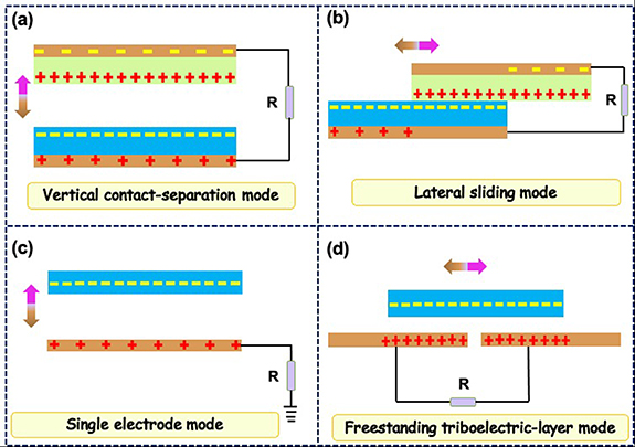
Figure 7. Four different modes of TENG. (a) Vertical contact-separation mode, (b) lateral sliding mode, (c) single-electrode mode and (d) freestanding triboelectric-layer mode. Reproduced from [23]. CC BY 4.0. © 2022 The Authors. Advanced Materials published by Wiley-VCH GmbH.
Download figure:
Standard image High-resolution imageIt has been reported that 2D materials have been used as the electrode, active triboelectric layer or both in the TENG. For any device, material with low internal resistance and high electrical conductivity is desirable to use as an electrode. These materials help in achieving a high production rate of induced charges in the TENGs [130]. Graphene offers excellent electrical conductivity and superior charge mobility, allowing electrons to travel without scattering up to a few micrometers [131–133]. The atomic thickness and large lateral size of 2D materials led to a high surface area to improve the effective contact area between the active layers of the TENG device. One such example is MoS2, which provides effective charge trapping sites due to the specific surface area and quantum confinement effects [66, 134]. In addition to enhancing the output performance of TENGs, the flexibility, optical transparency and mechanical stability of 2D materials also help in extending the applications of TENGs in e-skin, wearable electronics and optoelectronic devices [73, 76, 78].
4.1. TENGs with 2D materials as electrodes
The ever-increasing demand for flexible, foldable and wearable electronics, sensors and e-skin shifts the attention of researchers towards the development of flexible, portable and self-sustaining power sources. Flexible power sources, such as TENGs, can bend, fold, stretch and twist if designed with this type of active layer, electrode material and substrate. Active layer materials and electrodes can be tuned or modified to impart different functionalities to TENG including flame retardance. Some optoelectronic applications require transparent TENGs, where active layers, top and bottom electrodes and substrates essentially need to have high optical transparency.
Graphene has been explored as a transparent electrode for the fabrication of a high-performance flexible and transparent triboelectric nanogenerator (FTTG) [135]. Graphene as an electrode can offer low internal resistance and increase the rate of induced charges [130]. The performance of graphene was compared with the dominant flexible and transparent indium tin oxide (ITO) electrodes. Devices with monolayer graphene as the bottom electrode and ITO top electrode (IG); graphene as both top and bottom electrode (GG), and ITO as the top and bottom electrode (II) was fabricated (figure 8(a)). FTTG with a GI electrode produced the highest output of 56 V among all the electrode combinations. The output performance follows a trend of GI > II > GG > IG. The ITO is not suitable as a top electrode due to an increase in sheet resistance under applied strain [135]. The sheet resistance of graphene is much higher than that of ITO, which leads to a low output of the GG electrode combination. Thus, graphene as the top and ITO as the bottom electrode is the most suitable electrode combination for high output performance.

Figure 8. (a) Vertical contact-separation FTTG with different electrode combinations. [135]. John Wiley & Sons. © 2017 Wiley-VCH Verlag GmbH & Co. KGaA, Weinheim. (b) Transfer of touch into Morse code on a mobile device for assistive communication demonstration. Reprinted from [136], Copyright (2016), with permission from Elsevier. (c) Surface engineering process demonstrating the preparation of the electrode on PET sheet. Reprinted with permission from [137]. Copyright (2017) American Chemical Society. (d) Shear exfoliation and transfer process of shear exfoliated graphene. Reproduced from [138]. CC BY 4.0. © 2018 The Authors. Published by WILEY-VCH Verlag GmbH & Co. KGaA, Weinheim. And (e) vertical contact-separation mode TENG with LIG electrodes, PU and PI as the active triboelectric layers. Reprinted with permission from [34]. Copyright (2019) American Chemical Society.
Download figure:
Standard image High-resolution imageSimilarly, atomically thin graphene (<1 nm) was used as an electrode for the fabrication of a single-electrode TENG with polydimethylsiloxane (PDMS) as the triboelectric layer and PET as the substrate [136]. A TENG can attach conformally to human skin to produce output with contacts in different clothes. The fabricated device was demonstrated for assistive communication by transferring the touch into Morse code (figure 8(b)) on a mobile device. Later, the ability of CVD-grown graphene as a transparent electrode was improved by modifying it with conductive polymer poly(3,4-ethylenedioxy-thiophene) polystyrene sulfonate (PEDOT:PSS) [137]. Figure 8(c) schematically shows the surface engineering process to obtain the electrodes. The modified graphene exhibited 83.5% transmittance with 140% enhancement in the TENG's current density and 118% enhancement in the power. The enhancement in the output performance was due to the decrease in sheet resistance from 725 to 85 Ω sq−1 after PEDOT:PSS modification [137].
The liquid phase exfoliation to obtain an atomically thin layer of graphene offers low-cost and easy processability over CVD. However, the films deposited using liquid-phase exfoliation offer high resistance and generally require further modifications [138, 139]. To circumvent this issue, a facile method shown in figure 8(d) was used for the exfoliation of pristine graphene in water [138]. First, shear exfoliated graphene (SEG) was obtained at high shear mixing in water/sodium cholate solution. Later, isopropyl alcohol assisted direct transfer process was used for the transfer and assembly of SEG films. Water-exfoliated graphene can be transferred onto various substrates (paper, polymer, glass and Si) and used for the fabrication of single-electrode TENG (SE-TENG).
The other method to obtain graphene is irradiating a carbon source, such as polyimide (PI) or poly(etherimide), with a laser to convert the carbon to sp2 hybridized carbon [143, 144]. This process produces laser-induced graphene (LIG). LIG is a cost-effective approach offering ease of synthesis, stability and high conductivity [144]. The ease of processability makes LIG attractive for the fabrication of flexible TENGs. In this regard, PI was lased to form a high-performance LIG electrode for TENG. The LIG/PI TENG produced an output voltage of 3100 V in single-electrode mode with Al as the opposite contact layer [34]. The LIG was also used as an electrode in the vertical contact-separation mode TENG with PI and polyurethane (PU) as the active triboelectric layers (figure 8(e)). A 9 cm2 TENG device produces an output voltage of ∼1 kV. The direct write capabilities of LIG also allowed its transfer to the PDMS matrix for the fabrication of TENG. Similarly, LIG electrodes with a sheet resistance of ∼7 Ω sq−1 were used for the fabrication of a flexible triboelectric sensing array (TSA) for tactile sensing [140]. Figure 9(a) shows the fabrication process of 16 × 16 high-resolution TSA. The LIG was obtained on PI using a 10.1 μm CO2 laser. TSA works in single-electrode mode with silicone rubber as the active triboelectric layer. The TSA was used for the real-time detection and visualization of sliding, multipoint touch and finger motion [140].
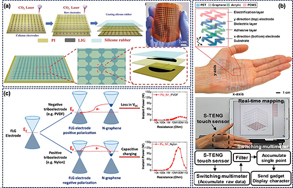
Figure 9. (a) Fabrication process of CO2 lased 16 × 16 triboelectric sensing array on polyimide. [140]. John Wiley & Sons. © 2021 Wiley-VCH GmbH. (b) Ultrathin conformally adherable S-TENG and the noise-reducing filter logic for real-time mapping. Reprinted from [141], Copyright (2019), with permission from Elsevier. And (c) mechanism for loss and gain in Voc when N-doped graphene was placed below negative and positive triboelectric layers. Reprinted from [142], Copyright (2021), with permission from Elsevier.
Download figure:
Standard image High-resolution imageAtomically thin graphene was also used as an electrode for the fabrication of an auxetically mesh-designed single-electrode TENG (S-TENG) [141]. The S-TENG with PDMS triboelectrification layer and PET substrate is shown in figure 9(b). The ultrathin (∼10 μm) S-TENG can be attached conformally for wearable applications and shows stretchability of 13.7% in the X-direction and 8.8% in the Y-direction. Figure 9(b) depicts the real-time mapping where the noise is reduced using a filter logic to display the number in trajectory mode. Recently, nitrogen-doped graphene was used as the interlayer between the triboelectric layer and the few-layer graphene (FLG) as an electrode to increase the capacitance [142]. An enhanced output TENG with nylon as the positive triboelectric layer and polyvinylidene fluoride (PVDF) as the negative triboelectric layer was designed. The use of N-doped graphene/PU as the interlayer below the nylon showed a 30% enhancement in the output power compared to TENG with PU as the interlayer. However, the performance of TENG decreases when the N-doped graphene/PU interlayer is placed below the PVDF layer. Figure 9(c) shows the mechanism for loss in Voc when N-doped graphene is placed with a negative triboelectric layer and an increase in Voc when placed below the positive triboelectric layer. The Fermi energy level (EF) shifts up for negative polarization of the FLG electrode and vice versa for positive polarization. For negative polarization, the capacitive charging of N-graphene is advantageous, and electrons will fill up in the conduction band of the N-graphene. For positive polarization, due to lowered EF, electrode depolarization and charge transfer occur from N-graphene to the FLG electrode leading to decreased Voc [142, 145].
The liquid GO dispersion was also used as the electrode in liquid single-electrode TENG (LS-TENG) [148]. The LS-TENG produced an output voltage of 123.1 V, a current density of 18.61 mA m−2 and a power density of 4.97 Wm−2. The liquid GO dispersion-based TENG was superior in performance (18.61 mA m−2) compared to NaCl-based electrode (1.8 mA m−2) and liquid metal electrode (8.6 mA m−2)-based TENG. Furthermore, the performance of LS-TENG (4.97 W m−2) was higher than that of solid GO electrode (3.13 W m−2) based on SE-TENG. The better performance was attributed to the presence of functional groups, effective charge transfer and electrical properties of GO [148]. However, the electrical conductivity of GO is poor compared to graphene.
The 2D metallic MoS2 nanosheets were combined with the 1D silver nanowires (Ag NWs) to attain high conductivity and flexibility for the fabrication of stretchable TENG (STENG), as shown in figure 10(a) [68]. The STENG (2.5 cm2) produced a power density of 0.16 W m−2 and was able to maintain stable performance under 50% stretching. The STENG is attached conformally to irregular surfaces such as plant leaves, as shown in figure 10(a).
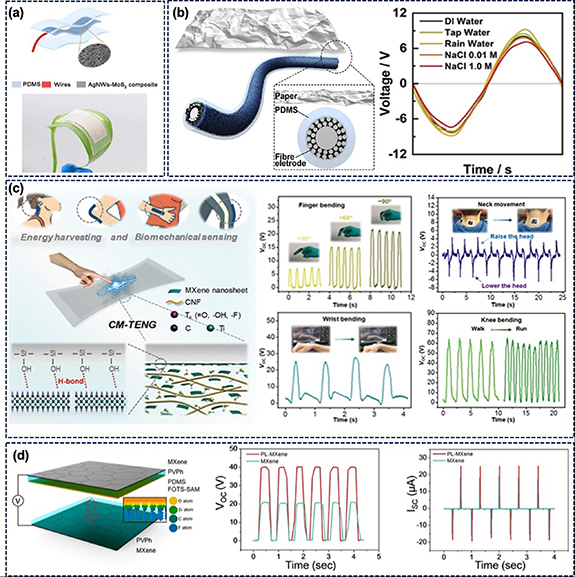
Figure 10. (a) AgNW-MoS2-based STENG and its conformal attachment to the irregular leaf surface. Reprinted from [68], Copyright (2019), with permission from Elsevier. (b) Ag nanoparticle-decorated MXene on yarn for TENG and variation in the output under different water (DI, tap, rain and NaCl). Reprinted from [74], Copyright (2020), with permission from Elsevier. (c) Shape-adaptive CM-TENG and the output under different biomechanical motions. [146] John Wiley & Sons. © 2020 Wiley-VCH GmbH. (d) 3D illustration of PVPh-coated MXene-based environmental stable TENG and the output comparison with and without coating. Reprinted with permission from [147]. Copyright (2021) American Chemical Society.
Download figure:
Standard image High-resolution imageMXenes (Ti3C2Tx ) offer excellent conductivity for use as an electrode. A yarn-based TENG was fabricated by coating the fiber with Ti3C2Tx MXene ink [74]. To further improve the conductivity, the Ag nanoparticles were decorated on MXene-coated yarn via electrostatic adsorption. Figure 10(b) shows the design of yarn-based TENG that produced an output voltage of 7.7 V. The TENG yarn was also capable of harvesting rain/DI/tap water as well as water containing NaCl, as shown in figure 10(b). Finally, to demonstrate the applicability of agrotextile, yarn was weaved into the textile to harness the water-flow energy. Later, Ti3C2Tx MXene/cellulose nanofiber (CNF) composite was used as the flexible liquid electrodes for TENG [146]. Figure 10(c) shows the overview of shape-adaptive CM-TENG for energy harvesting and biomechanical sensing. The 1D CNF plays the role of interlocking agent to improve the interconnections in MXene nanosheets. The CM-TENG generated an open-circuit voltage and short-circuit current of ∼300 v and 5.5 μA, respectively, due to the electron capability of MXene. Figure 10(c) depicts a few examples demonstrating the CM-TENG for self-powered biomechanical sensing. Recently, a thin polymer film of poly(4-vinylphenol) (PVPh) was spin-coated on a solution-processed MXene transparent electrode for protection against oxidation [147]. The PL-MXene electrode was used for the fabrication of environmentally stable TENG. Figure 10(d) shows PL-MXene-based TENG comprises FOTS-treated PDMS on a PL-MXene electrode and PL-MXene as the opposite layer. The device produced an open-circuit voltage of 40 V and a short-circuit current of 25 μA. The PL-MXene showed superior performance and stability over bare MXene (20 V, 17 μA). However, other polymers, such as ethyl cellulose, polymethyl methacrylate (PMMA) PVDF-TrFE were also explored for coating over MXene. All selected polymers based on TENG showed superior performance compared to bare MXene.
4.2. TENGs with 2D materials as an active triboelectric layer
Triboelectricity is ubiquitous and can happen between all materials including metals, biomaterials, nanomaterials, polymers, etc [149]. However, materials that lie far apart in the triboelectric series are always the choice of preference for the fabrication of high-performance TENGs [23, 150]. 2D materials offer high surface area, tunable work function and surface functional groups that makes them excellent candidates for active triboelectric layer as well as intermediate charge trapping layer [133].
In 2013, GO was reported for the fabrication of a multilayer TENG shown in figure 11(a) [151]. The multilayer structure comprises ITO/PI/GO on one side and Al/PI on the opposite side of the TENG (GONG). The GONG generated an output voltage and current of 2 V and 30 nA, respectively. The device without GO produced negligible output due to similar triboelectric layers in contact. Similarly, rGO was used as the electron-trapping interlayer below PI for the fabrication of enhanced output TENG (figure 11(b)) [152]. The rGO sheets accept electrons from donating diamine and behave as charge trapping sites. The TENF with PI:rGO layer showed 30 times enhancement in power density compared to that without PI:rGO layer. The rGO also worked as an electron-trapping site in the lateral sliding TENG.

Figure 11. (a) Design of GO film-based multilayer TENG. Reproduced from [151] with permission from the Royal Society of Chemistry. (b) 3D illustration of TENG based on rGO as electron-trapping layer. Reprinted from [152], Copyright (2017), with permission from Elsevier. (c) Fabrication process of AGS and PDMS composite film on conducting electrode. Reprinted from [153], Copyright (2017), with permission from Elsevier. (d) Exploded view of TENG based on MoS2 electron acceptor layer. Reprinted with permission from [66]. Copyright (2017) American Chemical Society.
Download figure:
Standard image High-resolution imageThe anti-corrosion, superhydrophobicity and self-cleaning properties of fluorinated graphene were utilized as the protective layer in the TENG [154]. The use of FC as an electronegative coating enhances the durability of TENG for water-wave energy harvesting under extreme alkali or acidic conditions. In another report, aligned graphene sheets (AGS) were mixed with PDMS (AGS@PDMS) for the fabrication of TENG [153]. Figure 11(c) schematically shows the fabrication process of AGS@PDMS-based TENG. The output performance of AGS@PDMS-based TENG was also compared with graphite particles and dispersed graphene sheets. The AGS exhibited a 1.44 times enhancement in the current compared to the disordered sheets. The TENG based on AGS, graphite microparticles and graphite nanoparticles produced an output current of 26, 13 and 14 μA, respectively. The AGS behaves as a plane-parallel microcapacitor to improve the overall device capacitance. Furthermore, a small gap between the AGS minimizes the dielectric loss and provides a maximum breakdown voltage [153].
Monolayer MoS2 was introduced as an electron acceptor layer into the PI triboelectric layer, as shown in figure 11(d) [66]. The TENG with MoS2 produced a power density of 25.7 W m−2, which is ∼120 times higher than that without MoS2. The large specific area of MoS2 imparts electron capture properties to MoS2 and charges are stored inside the layer to weaken the air breakdown effect. Thus, MoS2 effectively suppresses the electron and positive charge recombination. Following this, the contact-electrification behavior of MoS2, MoSe2, WSe2, WS2, GO and graphene (GR) was studied in order to propose the triboelectric series of 2D materials [155]. The TENGs were prepared in combination with different opposite materials including PDMS, polytetrafluoroethylene (PTFE), nylon, mica, PET and polycarbonate (PC) to perform the relative polarity test. Figure 12(a) shows the position of MoS2 revealed from the relative polarity test. Similarly, the positions of other 2D materials were revealed with respect to other triboelectric materials. Furthermore, Kelvin probe force microscopy was used to calculate the work function of 2D materials. MoS2 showed the highest work function (4.85 eV), followed by MoSe2 (4.70 eV), GR (4.65 eV), GO (4.56 eV), WS2 (4.54 eV) and WSe2 (4.45 eV). The output voltage of the nylon layer increases with increase in work function. However, WSe2 was the exception due to the difference in the surface roughness. Figure 12(a) shows a triboelectric series where 2D materials are included with respect to conventional polymers. The chemical doping process was also used to dope MoS2 with p-type gold chloride (AuCl3) and n-type benzyl viologen (BV) [156, 157]. The doping with AuCl3 increases the work function of MoS2, while BV doping reduces the MoS2 work function. The position of atomic scale 2D materials in TE series will broaden the application of TENG by paving a path towards thin and flexible devices. Later, a large CVD-grown MoS2 monolayer was used to fabricate flexible and bendable TENG [158]. The TENG with MoS2 showed better performance compared to those without MoS2. The MoS2/PS/ITO/PET TENG with PPy/PET top layer produced an output voltage of 18.4 V a current density of 1.8 μA cm−2 with a maximum power density of 33.1 μW cm−2. In addition, ferroelectric and non-ferroelectric PVDFs were introduced below the bottom layer (figure 12(b)). TENG I-MV is an ohmic contact, TENG II-MV is a Schottky contact and TENG III-MV is a p−n junction-based device. TENG III-MV produced the highest output of 80 V, 8 μA cm−2 and 455 μW cm−2 among all the devices. The best output of TENG III-MV was attributed to the synergistic effect of the ferroelectric PVDF layer and depletion layer. The Schottky and p−n junction device showed superior performance compared to the ohmic contact device due to the formation of a depletion layer by diffused charges [158]. MoS2 was also added as the lubricant layer to improve the wear resistance and surface charge density [159]. The durable TENG comprising polyvinyl carbonate (PVC)/MoS2 and polyamide (PA) as the active triboelectric layer produces an output voltage of 398 V and a short-circuit current of 40 μA. The 25 wt.% MoS2 leads to 19.4% (0.29) decrement in the frictional coefficient compared to pure PVC films. This work provides a new way of using 2D materials as a lubricant to improve the performance and life of TENG. Similarly, diamond-like carbon, MoS2 and Ti3C2Tx coatings were explored as protective films to improve the wear resistance of PTFE surface [160]. The MXene showed the best performance in vertical contact-separation mode due to the presence of oxygen and fluorine functional groups on MXenes.

Figure 12. (a) Arrangement of MoS2 using relative polarity test and triboelectric series of 2D materials. [155]. John Wiley & Sons. © 2018 WILEY-VCH Verlag GmbH & Co. KGaA, Weinheim. (b) Design of ohmic, Schottky and p−n junction-based TENG devices. Reprinted from [158], Copyright (2019), with permission from Elsevier. (c) 3D illustration of MoS2 quantum sheet-based TENG. Reprinted with permission from [67]. Copyright (2022) American Chemical Society. And (d) design of contactless TENG based on MoS2 incorporated LIG and its demonstration for touchless hand sanitiser. [161] John Wiley & Sons. © 2022 Wiley-VCH GmbH.
Download figure:
Standard image High-resolution imageThe N-doped biphasic MoS2−x Nx films were explored as electron acceptor layer in the TENG [162]. The N-doping increases the work function and surface roughness leading to superior performance, i.e. ∼three times enhancement over MoS2 alone. Later, MoS2 quantum sheets (QS) were also explored as a charge trapping layer to boost the output performance of TENG [67]. Figure 12(c) illustrates the 3D view of MoS2 QS-based TENG that generated peak-to-peak output voltage of 142 V, which is 2.7 higher than that without MoS2. Recently, MoS2-incorporated LIG was also demonstrated as a charge retention layer for contactless TENG based on Siloxene/Ecoflex, as shown in figure 12(d) [161]. The use of MoS2/LIG leads to a fourfold enhancement in the surface potential. MoS2/LIG as a charge trapping layer showed better performance compared to LIG and MoS2 alone as the charge trapping layer. Silicone/Ecoflex with a MoS2/LIG layer produced an output voltage of 31 V and a current density of 7 μA m−2. The best performance of MoS2/LIG was due to the improvement in the dielectric properties and better polarization effect. The device was demonstrated for touchless hand sanitizer to prevent the spread of COVID (figure 12(d)). The device was also demonstrated for controlling object motion in the game. Defect engineering of TMDs was also used to improve the performance of TENGs. In this regard, the process of thiol-ligand conjugation using different alkanethiols (mercaptopropionic acid (MPA); mercaptooctanoic acid (MOA); mercaptohexanoic acid (MHA) and mercaptoundecanoic acid (MUA)), as shown in figure 13(a) [163]. Figure 13(a) shows the design of WS2-TENG and the voltage output with different ligand conjugations. The MUA conjugation showed the most negative behavior and produced the highest output of 12.2 V among all other conjugations. The ligand conjugated (LC) WS2-TENG exhibited ten times enhancement in electrical performance compared to pristine WS2-TENG.
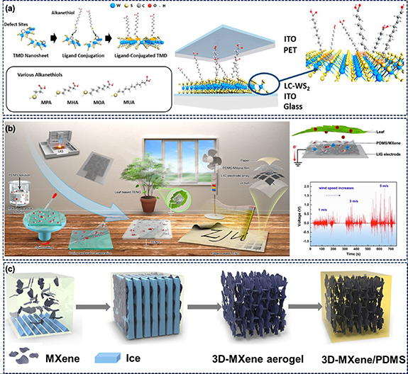
Figure 13. (a) LC of WS2 using various alkanethiols and the device design of LC WS2-TENG. Reprinted with permission from [163]. Copyright (2021) American Chemical Society. (b) Fabrication process of TENG with LIG electrode and PDMS/MXene composite layer and its demonstration for leaf swing energy harvesting. Reprinted from [164], Copyright (2019), with permission from Elsevier. And (c) freeze drying and vacuum impregnation process for the preparation of 3D-MXene/PDMS. Reprinted from [165], Copyright (2020), with permission from Elsevier.
Download figure:
Standard image High-resolution imageMXene attracted tremendous attention due to its high electrical conductivity and tribonegative properties superior to or comparable to Teflon due to the presence of the surface functional groups mentioned earlier. Ti3C2Tx is the most widely studied material of the MXene family and is used in all the works discussed below. Thus, MXenes can be used as an excellent triboelectric material and filler to boost the TENG performance. One such example is porous PDMS/MXene film with LIG as an electrode for the fabrication of flexible TENG [164]. Figure 13(b) illustrates the TENG fabrication process. The introduction of MXene increases the surface potential of PDMS from ∼−95 to ∼−301 V confirming the tribonegative behavior of MXenes. The MXene/PDMS TENG (MXene 15 mg ml−1) produced an output voltage of ∼119 V and an output current of ∼11 μA, which was sevenfold higher than pure PDMS. Figure 13(b) also depicts a device demonstration for harnessing leaf swing energy. The device was also demonstrated for human writing recognition. Likewise, a MXene/PDMS nanocomposite was prepared using a freeze-drying and vacuum impregnation method [165]. The method allows the formation of an interconnected MXene network (figure 13(c)). The 3D MXene/PDMS films were used to fabricate TENG with nylon as the opposite triboelectric layer, which produced an output of 45 V and ∼0.6 μA. The enhancement in output was not significant as pure PDMS produced 33 v and ∼0.2 μA. The reported method is complex with no significant advantage for TENGs. However, the films have a high thermal conductivity that can be used in thermal management.
Electrospinning, being a versatile technique with the advantage of a high surface-area-to-volume ratio of fibers, was explored for TENG active layer preparation. Furthermore, electrospinning offers an easy route to introduce different fillers to impart functionality to the fibers. In this regard, all electrospun active layer TENG based on PVA/MXene NF as a negative triboelectric layer and silk fibroin (SF) NF as the positive triboelectric layer was reported [166]. Figure 14(a) depicts the PVA/MXene and SF NF film fabrication process. The MXene-based TENG showed an exceptional output power density of 1087.6 mW m−2, which was used for body motion monitoring and powering electrowetting on a dielectric (EWOD) chip. EWOD chips are used for DNA analysis, environmental monitoring, cell manipulation and drug delivery. Similarly, MXenes were electrospun with PVDF-TrFE to obtain NFs with high surface charge density and dielectric constant [167]. The 10 wt. % MXene-loaded films exhibited the highest dielectric constant as well as dielectric loss. The enhancement in the dielectric constant is due to the applied electric field in the electrospinning process. The electric field creates microscopic dipoles providing better charge accumulation and charge storage. The fabricated EN-TENG produced an output voltage of 270 V, a transfer charge of 160 nC and a current density of 140 mA m−2. The EN-TENG was used to power stopwatches, LEDs and thermos-hygrometers. The EN-TENG was also demonstrated as a switch to trigger a door lock. Ti3C2Tx was also incorporated into PVDF to fabricate electrospun NF-based TENG [168]. The nylon 6/6 NFs were used as a positive triboelectric layer. The introduction of MXene improves the surface charge density and dielectric properties to enhance the TENG performance. In other work, MXene NF-based TENG was demonstrated to drive the MXene/TiO2/CNF heterojunction-based ammonia sensor.

Figure 14. (a) Electrospinning process of PVA/MXene and SF solution to obtain NF films. Reprinted from [166], Copyright (2019), with permission from Elsevier. (b) Device design of LC MXene/ZIF-67 TENG. Reprinted from [170], Copyright (2022), with permission from Elsevier. (c) Voltage output and device design of the TENG with and without h-BN buffer layer. Reprinted from [171], Copyright (2015), with permission from Elsevier. (d) Exfoliation and the coating process of BNNs for the fabrication of BoPET TENG. Reprinted from [172], Copyright (2021), with permission from Elsevier. (e) Fabrication process for CNF/phosphorene hybrid paper. [80] John Wiley & Sons. © 2017 WILEY-VCH Verlag GmbH & Co. KGaA, Weinheim.
Download figure:
Standard image High-resolution imageMXene (Ti3C2Tx ) was also extended to design fabric-based TENGs. The MXene/Ecoflex nanocomposite was coated on different fabrics to prepare FW-TENG [169]. The fabric texture, surface roughness using sandpaper and composite thickness were tuned to achieve the best performance. The 6 wt. % MXene loading generated the best output (780 V and 180 μA). The FW-TENG was able to harvest rain and wind energy. The MXene/PDMS was coated on fabric that was difficult to use for real-time applications considering the increase in fabric thickness, poor deformability and difficulty in integration with conventional textiles. Wash durability is another critical aspect that has not been explored. Later, porous laser carbonized (LC), MXene/ZIF-67 was introduced as an intermediate layer to enhance the output performance of fabric-based CNM-TENG (figure 14(b)) [170]. The LC MXene/ZIF-67 offers high surface area, excellent charge trapping properties and also improves the surface potential of the charge generating layer. The CNM-TENG produced an output power density of 65 W m−2. In addition, in non-contact mode, the TENG achieved a charge density of 15.3 μC m−2. CNM-TENG was demonstrated for numerous applications including gait monitoring, smart robots, and touchless wearable keyboards for powering electronic devices.
In 2015, h-BN was used to facilitate the deposition of high-κ dielectric Al2O3 on graphene [171]. The h-BN protects the graphene against oxidation and allows the deposition of high-quality Al2O3. A TENG using Al2O3/h-BN/graphene with graphene as the opposite layer was fabricated and compared with Al2O3 deposited without h-BN buffer layer (figure 14(c)). The Al2O3/h-BN/graphene-based TENG produced an output voltage of 1.2 V and a current density of 150 nA cm−2. The absence of the h-BN buffer layer allows the formation of AlOOH, which produces negligible output. Following this, pulsed laser deposition was used to obtain biphasic MoS2-hBN (2D/2D) composite thin films for the fabrication of TENG [77]. MoS2-hBN behaves as an electron acceptor layer with superior performance compared to h-BN and MoS2 alone. The MoS2-hBN produced an output voltage of ∼14.7 V, while h-BN and MoS2 produced an output voltage of 2.3 and 7.2 V, respectively. MoS2-hBN biphasic films have more trap sites for negative charges, endowing them with superior performance. Recently, in 2021, 2D h-BN nanosheets (BNNs) were coated on biaxially oriented PET (BoPET) for the fabrication of enhanced output TENG [172]. Figure 14(d) shows the exfoliation process and preparation of BNN coating on BoPET. The BNN/BoPET-based TENG generated an output voltage of 200 V, a current density of ∼0.48 mA m−2 and power density of ∼0.14 W m−2. The BNN/BoPET TENG exhibited 70 times enhancement in output power compared to the BoPET TENG. The enhancement in output was attributed to an increase in dielectric permittivity and electron accepting abilities of BoPET after BNN coating.
Phosphorene, a monolayer BP, offers high carrier mobility and exhibits excellent semiconducting behavior. Phosphorene has not been explored much for energy harvesting applications due to its poor environmental stability [173]. In an attempt to solve the problem, CNFs were used as a host to fabricate TENG based on tempo-oxidized CNF/phosphorene [80]. The CNF provides environmental stability to phosphorene. Figure 14(e) shows the fabrication process of CNF/phosphorene hybrid paper, which remains stable for 6 months under ambient conditions. The CNF/phosphorene TENG produced five (5.2 V) and nine times (1.8 μA cm−2) improvement in the voltage and current density compared to pure CNF paper-based TENG.
In 2019, MOFs were reported for the first time for the fabrication of TENGs and self-powered tetracycline sensing [53]. Since then, MOFs and COFs have garnered attention for energy harvesting due to their exceptionally high surface area, tunable porosity and ease of post-synthetic modifications [83]. The majority of MOFs/COFs reported for TENG are 3D structures and only a few of the MOFs/COFs crystallize in a layered structure. One such example is Co/Zn bimetallic framework (BMOF), which forms elliptical nanosheets [174]. A BMOF-TENG was fabricated based on Co/Zn BMOF nanosheets coated on conductive fabric (BMOF/FCF) as the tribopositive layer and PTFE as the tribonegative layer. Figure 15(a) shows the synthesis and coating of Co/Zn BMOF on textile and its flexibility. The output of BMOF-TENG increases with an increase in the Zn content of Co/Zn BMOF. The 15% Zn content produced the highest output of 47 V and 7 μA, which is ∼450% enhancement in the TENG performance. The BMOF-TENG was demonstrated for ammonia sensing at room temperature (figure 15(a)). Figure 15(a) also shows the ammonia-sensing mechanism. BMOF offers adsorption sites that change the number of available electrons and thus the resistance of BMOF. BMOF is an n-type material whose resistance decreases when exposed to reducing gas.

Figure 15. (a) Synthesis of Co/Zn BMOF, its coating on conducting fabric for the fabrication of TENG and the ammonia-sensing response with the mechanism. Reprinted from [174], Copyright (2021), with permission from Elsevier. (b) Device fabrication process of GTNG. [39] John Wiley & Sons. © 2014 WILEY-VCH Verlag GmbH & Co. KGaA, Weinheim. (c) R2R growth and hot water delamination process to transfer graphene on EVA/PET. [33] John Wiley & Sons. © 2015 WILEY-VCH Verlag GmbH & Co. KGaA, Weinheim. (d) 3D illustration of CG-TENG with spring spacer. Reprinted from [175], Copyright (2019), with permission from Elsevier. And (e) voltage output and the corresponding device designs for comparing the performance of MXene with PTFE. Reprinted from [75], Copyright (2018), with permission from Elsevier.
Download figure:
Standard image High-resolution image4.3. TENGs with 2D materials as both active triboelectric layer and electrode
Some 2D materials, such as graphene and MXenes, can play dual roles, i.e. electrodes as well as active triboelectric layers due to high electrical conductivity, large surface area and the presence of functional groups. In 2014, large-scale CVD-grown graphene was used to fabricate TENGs (GTNGs). Different graphene transparent layers, i.e. monolayer (1L), randomly stacked bilayer (2L), trilayer (3L) and quad layer (4L) as well as Bernal stacked graphene, were used in GTNGs [39]. The 1L graphene transferred onto PET also serves as the top electrode. Figure 15(b) shows the GTNG fabrication process. The 1L GTNG showed better performance with an output voltage of 5 V and a current density of 500 nA cm−2. The difference in output can be attributed to the work function and frictional differences. The friction varies with the number of graphene layers due to the electron-phonon coupling and puckering effect. However, the regularly stacked graphene layer showed superior performance (9 V, 1.2 μA cm−2) compared to 1L graphene.
The roll-to-roll (R2R) technique can be used to transfer CVD-grown graphene onto different flexible substrates. The R2R green transfer process was used to transfer graphene onto ethylene vinyl acetate EVA/PET film (figure 15(c)) for the fabrication of TENG [33]. The method was clean and eco-friendly as the complete process was realized using water with no involvement of any toxic etchant. The TENG device comprises graphene/EVA/PET as the upper layer and PDMS/graphene as the bottom layer. Graphene serves as an electrode as well as an active triboelectric layer. The TENG produced an output voltage of 22 V and a current of 0.9 μA.
Crumpled graphene (CG) offers surface roughness and a high work function controllability to improve the performance of TENG [175]. A vertical contact-separation-mode TENG (CG-TENG) consisting of PDMS and CG as the triboelectric layer with spring spacer was fabricated [175]. The CG also serves as an electrode for the top PDMS layer, as shown in figure 15(d). The CG-TENG produced an output voltage, current and power density of 83 V, 25.78 μA and 0.25 mW cm−2, respectively. Furthermore, the performance of TENG was directly related to the crumple degree of graphene, which increases the effective contact area, work function difference and surface area. The CG-TENG was also modified into a stretchable device by replacing the spacers. The stretchable TENG produced 78.5 V at = 0%, which was reduced to 41.4 V at = 120%. A stretchable TENG was employed to test the finger bending angle and bending rate [175]. CG was also reported for the fabrication of small-size stretchable TENGs with high output performance, where silicone was used as the opposite triboelectric layer [176]. The stretchable TENG can work under stretching, compression and in hybrid mode. The beauty of stretchable CG-TENG fabricated in this work is that there is no significant change in the output even at 200% strain [176]. Recently, in 2022, the work function of graphene was tuned using a defect-mediated strategy (DMS) to fabricate high-performance TENGs. Different oxygen content and carbon defects in graphene were achieved using annealing temperatures in the range of 500 °C–3000 °C leading to a tunable work function from 4.68–4.49 eV. An annealing temperature of 2000 °C produced the lowest work function of 4.49 eV corresponding to a maximum output of 190 V and 14 μA. DMS is an effective strategy to tune 2D materials for enhanced TENG performance.
Excellent conductivity and surface properties of Ti3C2Tx were used for the fabrication of a single-electrode mode TENG [75]. Figure 15(e) depicts three single-electrode mode TENGs for the comparison of MXene with PTFE. The MXene TENG and PTFE TENG showed similar performance in single-electrode mode. The nearly zero output between MXene and PTFE suggests a similar behavior for the materials in contact. In the contact separation mode, the ITO-MXene and PET-MXene interface pairs generated an output voltage of 650 V and a power density of 400 mW m−2. The device produced an output of 40 V when clamped at 30° [75]. Table 2 shows the performance comparison of 2D material-based TENG.
Table 2. The output performance of TENGs based on 2D materials as electrodes, active layers and both as electrodes and active layers.
| Functionality | 2D material | Active layer | Voltage (V) | Current or current density | Power density or power | References |
|---|---|---|---|---|---|---|
| Electrode | Graphene (G) | PI-PET | — | — | 101 mW m−2 | [135] |
| PDMS | 47.1 | 7 μA | 144 mW m−2 | [136] | ||
| PDMS | 4.98 | 0.52 μA | — | [138] | ||
| PDMS | 15.1 | 4.7 μA | 360 mW m−2 | [141] | ||
| PI-Al | ∼3500 | ∼60 μA | ∼2400 mW m−2 | [34] | ||
| GO | PDMS | 123.1 | 16.7 μA | 4975 mW m−2 | [148] | |
| MoS2 | PDMS | 95.8 | — | 160 mW m−2 | [68] | |
| Active layer | Graphene | Al-PI | — | — | 6300 mW m−2 | [152] |
| Cu-G/PDMS | 117 | 26 μA | 4800 mW m−2 | [153] | ||
| G@PDMS | 2 | 0.002 μA | — | [177] | ||
| GO | GO@SDS@PDMS | 438 | 55 μA | 4800 mW m−2 | [178] | |
| Carbon aerogel composite | 80 | 0.03 μA | 0.4 μW | [179] | ||
| MoS2 | Al-PI@MoS2@PI | 400 | — | 25 700 mW m−2 | [66] | |
| MoS2-PP | 7.2 | 0.52 μA | 276.3 mW m−2 | [77] | ||
| MXene | SF-MXene@PVA | — | — | 1087.6 mW m−2 | [166] | |
| BP | Au-BP@CNF | 5.2 | 18 mA m−2 | 10.6 mW m−2 | [80] | |
| Both electrode and active layer | Graphene | PET-G | — | — | 25 mW m−2 | [39] |
| PDMS-G | — | — | 2500 mW m−2 | [175] | ||
| MXene | PET-MXene | 650 | — | 400 mW m−2 | [75] | |
| Graphene-MXene | Paper-MXene@PDMS | — | — | 609.1 mW m−2 | [164] |
5. 2D material-based photovoltaics
Incorporation of inorganic 2D nanomaterials for the development of solar PVs holds great promise for future renewable energy technologies [31, 180–182]. 2D nanostructures possess unique advantages, such as high optical transparency, electrical conductivity, high absorption, tunable band gap, mobility, charge carrier lifetimes and flexibility as discussed earlier. Recent developments in this area have led to a wide variety of atomically thin layered materials including graphene, h-BN, transition metal dichalcogenides (TMDs-MoS2, WSe2 etc)), MXenes (Ti3AlC2), BP and silicene [27, 183]. These material systems meet the crucial requirements of third generation solar cells, such as efficient photon absorption, wide electronic band structure, generation and separation of charge carriers, stable performance, sustainability and scalability [184, 185]. Some of these features are much better than the previous generation PV cells that used single crystalline and thin films of semiconductors as active layers. For instance, monolayer graphene has shown the best reported optical transparency as it absorbs only 2.3% of sunlight in the visible region with minimal reflectance of ∼0.3%. In comparison, the same optical transparency metric can be attained only with an equivalent Si thickness of ∼20 nm, which has practical development constraints. This has paved the way for the potential replacement of ITO transparent conductors with graphene in solar cells. Graphene as a transparent conductor has been tested for organic PVs, thin films and Schottky junction solar cell, which has been observed to perform on par with traditional films of ITO and fluorinated tin oxide [31]. 2D TMDs are attractive candidates since they possess tunable electrical characteristics of semimetals, semiconductors and superconductors. Bulk MoS2 displays an indirect band gap of 1.3 eV, which exhibits a direct band gap of 1.8 eV in its ultrathin monolayer form. Due to these attributes, the optical absorption of MoS2 falls in the range of 5%–10%, which allows it to be utilized as an active component in PV cells [186]. The crystalline quality, areal coverage and number of layers play a key role in incorporating TMDs in third generation solar cells. PV cell architectures including p–n junction (WSe2/n-type ZnO) and Schottky junction (WSe2/Al) have demonstrated PCE in the range of 5%–6%, which is currently being studied for future enhancement. Parallel developments in organic PVs have gained significance due to their effective utility in flexible and wearable electronics systems, which are used largely under ambient outdoor conditions [187]. Graphene, MoS2 and BP were used as charge transport layers in organic PVs where their role was to swipe the photo-generated charge carriers efficiently from the bulk organic heterojunctions and transport them to contact electrodes. These cells were meant to perform under multiple bending conditions and produced moderate PCE in the range of ∼8%. Similarly, perovskite solar cells (PSCs) are projected as potential alternatives for Si PVs in the future where layered 2D structures have been incorporated as charge carrier transporters, conducting electrodes and stabilizers. PSCs are the frontrunners in the current PV developments, with the PCE already exceeding 20%, and it is expected that during the current decade cell performance will improve with the extended application of 2D materials [188–190]. Recently, 'all 2D solar cells' have gained significant attention due to their strong interactions with light, along with a tunable band gap [191]. Novel 2D heterostructures, such as MoS2/graphene and MoSe2/WSe2 form sharp interfaces with good light absorption characteristics (∼10%), which paves the way to produce ultra-thin PV cells with demonstrated PCE in the order of 5%. Figure 16 shows the comprehensive illustration of the four categories of solar cells, (a) graphene and TMD/Si PVs, (b) organic PVs, (c) PSCs and (d) 2D heterostructure PVs. The incorporation of 2D materials into these PVs enhances their performance through their unique structure and properties. The subsequent sections explain the cell architecture of these PV types and the role of 2D components along with recent progress to improve overall efficiency.
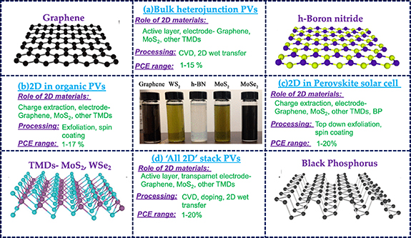
Figure 16. Schematic illustration of the overview and role of emerging 2D materials in the development of third generation solar cells. Photograph in the middle row shows the exfoliated wide 2D materials for spin coating. [191] John Wiley & Sons. © 2018 WILEY-VCH Verlag GmbH & Co. KGaA, Weinheim.
Download figure:
Standard image High-resolution image5.1. Graphene and TMDs in bulk solar cells
The highly successful Si PV technology is based on p–n junction, which creates an energy barrier across the interface to separate the photogenerated charge carriers. Graphene is known to be a semimetal with zero band gap and is observed to form a Schottky junction with n-type Si to develop solar cells (figure 17(a)). Graphene/ Si PV stack is prepared by a wet transfer process of CVD-grown graphene with a SiO2 separation layer and metal contact on opposite sides [192, 193]. The formation of graphene/n-Si Schottky junction followed by Fermi-level band alignment leads to a built-in potential across the interface. This built-in voltage is developed due to the diffusion of electrons from Si towards graphene, which creates a depletion region with a barrier for the transportation of the majority carriers. The built-in potential is much smaller than the conventional Si p–n junction but provides two effective scenarios for the photogenerated charge carriers. They are as follows: (1) an electron–hole (e–h) pair is generated in Si when the incident photon energy is higher than the band gap and the charge carriers separated by holes (h+) move to the graphene layer with electrons bound in Si, (2) an e–h pair generated in graphene when the incident light energy is higher than the Schottky barrier but lower than Si. This PV cell architecture has shown an OCV of ∼0.5 V and a PCE of 1%–1.7% when a study was conducted, initially in 2010. Over this period, the cell structure has gone through fine modifications, such as doping of graphene, integrating a layer of TiO2 antireflection coating and tuning of Si native oxide thickness (5–20 A˚), which led to the demonstration of PCE of 15.6% with Voc of 0.6 V. These values are on par with the commercial Si PV technology. This cell uses a lightly doped (2–4 Ωcm) n-type Si wafer as a base with the following advantages compared to conventional Si PV|: (a) low-cost graphene transfer (b) overcoming the high-temperature diffusion doping process, (c) graphene serves the dual role of photoactive junction layer for hole collection as well being a highly transparent conductor. The problems associated with traditional ITO transparent conductors (i.e. drained resources, long-term stability and cost) can be addressed by replacing graphene in solar cells. The lack of band gap and low Schottky barrier prompted us to utilize TMDs as a photoactive layer in PVs due to their intrinsic properties. CVD-grown monolayer MoS2 (t ∼0.65 nm) transferred to a bulk p-Si substrate over an area of 1 cm2 with an Al electrode (t-15 nm) on the top layer for ohmic contact and optical transparency [194, 195]. The n-MoS2/p-Si cell structure displays a type II heterojunction with illumination and demonstrated a Voc of 0.2 V and a PCE of 5.23%, which is quite promising for further improvement (figure 17(b)). The light absorption in this cell architecture can be improved by multiplying the number of 2D layers, which has a negative effect as the band gap is altered to an indirect one. In addition, the existence of surface states and defects are the deteriorating factors that affect the built-in voltage at the MoS2/Si p–n junction, which has been countered by introducing an Al2O3 passivation layer over the 2D layer. With these features incorporated, CVD-grown MoS2 film active layer PV cell has demonstrated robustness in terms of repeatable output with a PCE of 5.6% with an Al2O3 passivation layer. These developments set platforms to incorporate other 2D TMDs as Si heterojunction solar cells for future applications.
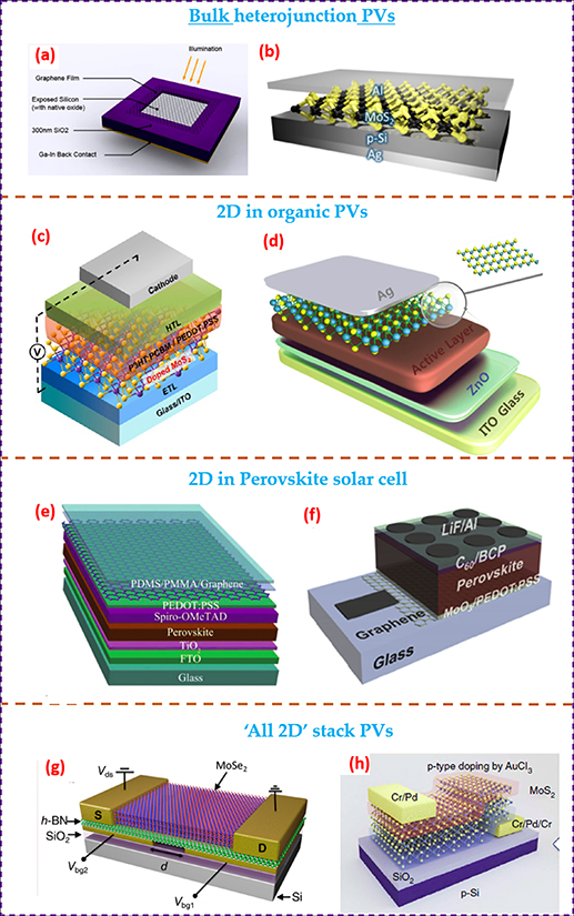
Figure 17. Illustration of four different types of solar cell architectures using the 2D materials through the different state-of-the-art processing techniques. Bulk heterojunction (a), (b) and 'all 2D' stack solar cells use as active photoactive and electrode layers. Reprinted with permission from [192]. Copyright (2015) American Chemical Society. Reprinted with permission from [195]. Copyright (2014) American Chemical Society. OPV (c), (d) and PSC. Reprinted with permission from [187]. Copyright (2013) American Chemical Society. [197] John Wiley & Sons. Copyright © 2013 WILEY-VCH Verlag GmbH & Co. KGaA, Weinheim. (e), (f) Cells mainly utilize them as charge extraction layers as well as transparent conductors. [31] John Wiley & Sons. © 2018 WILEY-VCH Verlag GmbH & Co. KGaA, Weinheim Reprinted from [199], Copyright (2019), with permission from Elsevier. (g), (h) 'all 2D' heterostructures based vertical p-n junction solar cells [191] John Wiley & Sons. © 2018 WILEY-VCH Verlag GmbH & Co. KGaA, Weinheim.
Download figure:
Standard image High-resolution image
5.2. Role of 2D materials in organic PV
Organic solar cells have gained significant advantages among the third generation PV developments due to the merits of low cost, being lightweight and having inherent flexibility [196]. The organic photovoltaic (OPV) cell structure consists of a separate electron and hole extraction layer along with OPV layers and electrodes (figures 17(c) and (d)). A variety of 2D materials play crucial roles possibly in all the layers to provide enhancement in either bulk or layered heterojunction OPVs. The photogenerated excitons (e–h pair) possess high binding energy (0.1–1 eV) and low diffusion length (1–10 nm). In addition, organic materials suffer from a narrow light absorption band (100–200 nm) [31]. These issues are prompting us to incorporate inorganic 2D materials into OPVs to improve cell outputs without losing their inherent advantages. The commonly used photoactive polymer material consists of poly(3-alkylthiophenes) P3HT: ([6,6]-phenyl-C61-butyric acid methyl ester) (PC61BM) (P3HT: PCBM), which form heterojunctions of electron donor–acceptor components. The photo-generated electrons from this junction are extracted using inorganic materials, such as ZnO, TiO2, etc, and the holes are transported most commonly by poly(3,4-ethylenedioxythiophene) doped with poly(styrene sulfonate) (PEDOT: PSS)). The charge carrier transport layer is expected to have high mobility and a low work function to conduct the electrons efficiently to the cell's outer electrodes. 2D materials, such as graphene, MoS2 and BP meet the layer requirements (band gap, mobility, transparency) along with low-temperature processing conditions. PEDOT: PSS is a widely used p-type conductor in OPV devices. It is hygroscopic and tends to corrode photoactive and electrode materials. Doped p-type TMDs (MoS2 and WS2) are potential replacements as hole transport layers, which are more stable compared to PEDOT: PSS to make efficient hole extraction [187]. A typical OPV structure consists of ITO/ZnO/photo active bulk junction polymer ((P3HT: PCBM))/PEDOT: PSS/Ag, which produces PCE in the order of 1%–3%, as seen largely from previous works. Recenty, novel OPV stack processing has demonstrated that cell performance metrics can be pushed towards being on par with Si PV by benefiting from 2D materials. Notably, the chemical exfoliation of MoS2 sheets from Lix MoS2 via ultrasonication followed by dispersion in alcohol solvent proves an efficient methodology to produce high-quality layers for hole extraction. A few layers of MoS2 spin coated on Ag conductive electrode with PTB7:PC71 BM active layer produced an output Voc ∼0.7 V and a PCE of 8.11%. This significant improvement is achieved by making use of 2D materials as hole extraction layers [197]. A similar top-down method has been used for bulk commercial powders of MoS2 and WS2 to prepare a suspension of 2D sheets followed by spin coating to demonstrate high-efficiency OPVs. The spin-coated WS2 on the ITO film was used for hole extraction from the bulk heterojunction of semiconducting ternary compound PBDBT-2F:Y6: PC71BM (PBDB-T-2F:Y6: [6,6]-phenyl-C71-butyric acid methyl ester) (PC71BM)). This architecture has demonstrated that one of the highest recorded PCEs of 17% and Voc of 0.84 V with WS2 2D layers plays an active role as a hole extraction layer [198]. BP is an emerging 2D material that has been shown to act as an effective charge transporting interlayer in OPV due to its attractive physical properties, such as its high mobility (1000 cm2/V-s), band gap and anisotropic structure. Chemical exfoliation followed by spin coating of thin BP in a PTB7:PC71BM active-layer solar cell as an interface layer helped to improve the PCE in the range of 8%–11%. This has been attributed to the cascaded band gap of BP, with other charge transporting materials, such as ZnO and PEDOT: PSS. While graphene has always been a material of choice for many components of OPVs, the advent of a new class of 2D systems with interesting physical properties provides ample opportunities to develop highly efficient, flexible low-cost solar cells.
5.3. 2D materials for PSCs
PSCs are emerging as an important class in PV cell development with consistent demonstrations of PCE in excess of 20% where cell architectures share notable similarities with OPV [189, 199, 200]. They are projected for the future with high hopes of competing with commercial Si technology. The photoactive layer in PSC is an organic-inorganic hybrid generally denoted by ABX3, where A refers to CH3NH3, B is a cation (Pb/Sn) and X is halogen (Cl, Br and I) where one of the widely studied solar cell compounds is methyl ammonium lead iodide (CH3NH3PbI3). The perovskite active layer is sandwiched between the electron and hole transporting layer similar to OPV cells (figures 17(e) and (f)). The band structure is created by Pb/I atoms and the methylammonium cation contributes to the formation of a 3D perovskite lattice. It holds a direct band gap (1.55 eV) with a large light absorption coefficient over a wide light spectrum, which takes control of efficient light-harvesting followed by charge carrier generation [201, 202]. The ability to tune the optical band gap by altering the cation/halogen component and attain more stable optical absorption keeps the PSCs ahead of the OPVs to achieve higher efficiency. 2D materials have been reported to serve to constitute an ultrafast electron and hole transport layer in PSCs, which helps to achieve high PCEs. 2D TMDs, such as MoS2, WS2 and BP prepared using top-down chemical exfoliation followed by spin coating on mixed halide perovskite CH3NH3PbI3–xClx act as efficient interlayers for highly efficient stable PSC performance. Typical hole extraction layers in such PSCs are prepared using PEDOT:PSS or commercial Spiro-OMeTAD, which inflicts iodine diffusion across perovskite active material into the hole extraction layer, which affects the stability of the cell through degradation [188]. In addition, this will lead to the perovskite layer making contact with the outer electrode with the possibility of photogenerated charge carriers recombining before being extracted from the cell. These technical bottlenecks of PSCs have been effectively solved by making use of 2D TMD interlayers between photoactive and charge carrier extraction layers. The spin-coated MoS2 flake interlayer at the interface of MAPbI3/ Spiro-OMeTAD (HEL) have demonstrated PCE of 13% without degradation for the tested duration of 550 h. The same device stack without a MoS2 charge extraction interlayer has shown a PCE of 7% with device degradation of 34%. The incorporation of MoS2 has passivated the perovskite surface to prevent iodine diffusion and provided a suitable energy-level alignment for efficient charge carrier transportation without recombination. Further attempts to use TMDs as interlayer and stand-alone carrier extraction layers have helped to push the PSC PCE towards 20%. One notable recent effort in PSC is graphene-perovskite panels that utilized graphene and MoS2 in electron and hole extraction layers and further demonstrated large-area (4.5 m2) perovskite panels as a direction towards outdoor installation from laboratory model [29]. In this system, the basic cell consists of TiO2 as the electron transport layer with the addition of a graphene enhancer and poly(triaryl amine)/MoS2 combination layer for hole extraction. For each unit, if the solar cell has an area of 11 × 11 cm2 (active area ∼9.1 cm2) and a total of 360 modules have been connected, this demonstrates the potential scalability of this development. This significant step towards the installation of a consumer utility has covered a panel solar farm area of 4.5 m2 with peak power of more than 250 W. The cell produced a PCE of 11%, which has huge scope to improve further beyond 20% and produce solar farms in the upcoming decades.
5.4. 2D heterostructure-based PVs
The unprecedented development of a wide variety of 2D materials has shown the fabrication pathways to develop 2D heterojunctions both in the lateral and vertical directions. The evolution of PV technology development started with bulk Si followed by thin films with organic and hybrid active layers. The evolution of 2D materials has provided the pathway to produce an 'all 2D stack' solar cell for future energy applications [28, 203, 204] (figures 17(g) and (h)). (This provides the possibility of developing the thinnest possible PV cell along with the merit of attaining the high energy density per unit mass of the PV cell compared to the previous generation cells) [191]. 2D materials overcome all the technical shortcomings of the previous generation, such as high absorption over a wide optical range, tunable band gap, efficient photogeneration followed by transportation, stable materials under service, light weight, high transparency, low cost and scalable cell development process. The two choices for 2D junctions are as follows: (1) lateral heterostructure; the built-in potential is created along a 1D edge where the electric field is parallel to the 2D crystal plane and (2) vertical junction by fabricating a layer-by-layer stack where the built-in electric field acts perpendicular to the 2D plane. Novel attempts have been made to create lateral doping-free p–n junction of 2D TMDs and extract the photo response from the layer. The lateral p–n junction of WSe2 is produced by making use of the bottom split gate configuration fabricated on high-k dielectric layers of HfO2 and SiN [205]. Opposite charge carriers are generated by applying opposite biasing at two (split) gates simultaneously. A lateral rectifying behavior is observed on opposite sides of monolayer WSe2 with a photo response. The device was illuminated using a halogen lamp (140 mW cm−2) and showed a PCE of 0.5% with Voc of 0.87 V. The split gate configuration was further improved by engineering the stack with different 2D materials, dielectrics and metal electrodes. WSe2 is a highly transparent (∼95%). TMD has been tried as a lateral p–n junction using a split gate approach with h-BN 2D layers as a gate dielectric in the stack. It has been realized that a junction with multilayers leads to higher photovoltaic current to produce higher PCE. This has been well understood by creating a multilayer WSe2 active layer lateral p–n junction through a split gate to enable a PCE of 14%, which is on par with the likes of organic and hybrid PVs. This demonstration illustrates that the other means of creating p–n junctions (e.g. doping and lateral heterojunction) are potential pathways to realize high-efficiency 2D PVs. Vertically stacked 2D layers offer innovative PV cell configurations that have achieved performance comparable to current PV generation cells. The 2D vertical configuration provides engineered stacking options for homojunction, heterojunction (type I–III) and vdW heterostructures. Doping of MoS2 layers using AuCl3 (p-type) and benzyl viologen (BV-n-type) has helped with the fabrication of 2D vertical p–n junction and the study of the photovoltaic behavior of the cell stack [206]. With an effective doping layer depth of 1.5 nm and a junction depth of 3 nm we have produced Voc of 0.6 V and a PCE of 0.4%. With the advent of new 2D materials, many options are being tried in the 2D/2D vertical configuration that do not pose lattice mismatch stress issues as in thin epitaxial films, which hamper the device performance. The low PCS of 'all 2D stack' PVs is largely attributed to the thickness-dependent adsorption, which can be addressed by incorporating a nanoparticle layer to improve plasmonic effects. With the early stage of development, improving the stack configuration with efficient charge generation and transport, an appropriate 2D vdW stack and energy band matched metal contact will help to achieve higher PCEs.
6. Conclusion, challenges and future perspective
2D materials have been widely explored for energy harvesting applications. This review entails research on 2D materials for PENG, TENG and PV. Exciting features of 2D materials include tunable work functions and band gaps, excellent flexibility and electrical properties. Furthermore, the surface, electrical and optical properties of 2D materials can be altered by surface functionalization, change in dimensions and phase. Despite significant efforts, the relationship between process, structure, properties and performance beyond graphene and MoS2 is in the early stage. The challenges associated with 2D materials include the following:
- 1.The 2D materials are investigated in detail for energy harvesting including PENG, TENG and PV. The properties of 2D materials including high transparency, electrical conductivity, high absorption, tunable band gap, mobility, charge carrier lifetimes and flexibility are the reasons behind the tremendous research in the field. 2D materials, such as MXene, have the potential to replace conventional electrodes in electronic devices. In TENGs, these materials can lead to high surface area, and functional groups like fluorine on the MXene can produce high output. However, the large-scale growth, synthesis and manufacturing of most 2D materials beyond graphene is still in its infancy and poses significant challenges. The key requirement is a cost-effective transfer of large-scale, high-quality 2D films onto the substrate while achieving controlled thickness and dimensions. Currently, hydro or solvothermal synthesis, liquid-phase exfoliation and growth techniques, such as CVD, physical vapor deposition (PVD) and molecular beam epitaxy (MBE), are widely used for the process and growth of 2D materials [207]. Hydro and solvothermal methods and liquid-phase exfoliation are cost-effective methods, but they fail to deliver controlled thickness, size and quality of the 2D material. CVD, MBE and PVD can produce high-quality 2D materials with controlled thickness. However, growth techniques generate low yield, are expensive and have stringent requirements on vacuum, temperature and substrates [207]. A low-cost, easily processable large-scale manufacturing method is a much-needed step-up change required to extend 2D materials for energy harvesting applications.
- 2.
- 3.The majority of 2D materials have not been studied in detail to establish their cytotoxicity and biocompatibility. 2D materials have been reported for numerous applications including energy harvesting, sensing and wearable electronics. Energy harvesters, especially PENG and TENG, are well known for harvesting low-frequency motions, such as biomechanical energy, where the device comes into human contact, and these devices are also implanted in animal models for various applications. However, the long-term in vivo and in vitro cytocompatibility studies beyond graphene are still in the early stage and require huge attention considering human and environmental safety [210–212]. Further surface functionalization, modification and dimensional change can alter the cytotoxicity of the materials. Thus, it is important to systematically investigate the effect of 2D materials on humans via in vivo and in vitro studies. Moreover, cytotoxicity is concentration-dependent and a database containing the safe concentration of 2D materials is very helpful for the applications of 2D materials where living organisms are involved.
- 4.The performance of the majority of 2D materials is far below that compared to the state-of-the-art materials, such as polymers for TENG and ceramics for PENG. Recently explored MXene (Ti3C2Tx ) showed triboelectric performance comparable to or similar to the most triboelectric-negative material Teflon [75]. Approaches, such as surface functionalization, modifications, and defect and strain engineering, can be used to improve the energy harvesting performance of 2D materials. In the case of TENG, surface functionalization or modification with small molecules can improve the surface charge density, thereby improving the material figure of merit [213]. Alternatively, hybrid devices combining PENG, TENG and PV can be used to design high-performance devices. The PENG-TENG hybrid using a single material has already confirmed the possibility of enhancing the device performance [214].
- 5.Discontinuous output of PENG and TENG cannot be used directly to drive electronics, sensors or any other components. It is essential to store the output generated from energy harvesters in a storage unit (supercapacitor or battery) [215–217]. Integration of the energy harvester and the energy storage unit requires intermediate circuits leading to power loss. In addition, external circuits are not flexible and hinder the applicability and miniaturization of the overall system. Moreover, low output power from 2D energy harvesters requires combining multiple energy harvesters to enhance the power density. The energy harvesters have different impedances causing the problem of impedance mismatch for device integration. In 2015, the concept of a self-charging supercapacitor power cell (SCSPC) was introduced for creating an all-in-one system [218]. Since then, numerous internal and external SCSPCs have been reported. However, charging the storage unit to a voltage of 1.5–2 V in a short time is still challenging. Several attempts have been made to enhance the performance of the storage unit by replacing the electrolyte to improve the device packaging for long-term stability. The continuous developments and advancements in both energy harvesting and storage may soon lead to the development of an effective all-in-one system.
Most 2D materials have been investigated theoretically or experimentally for the demonstration of piezoelectricity, but the majority of them have not been demonstrated for energy harvesting applications. MOFs are multifunctional materials that have been demonstrated for TENG-based self-powered sensing and the enhancement of β-phase in the PVDF for PENG [219]. However, many MOFs exhibit a non-centrosymmetric space group indicating the presence of potential piezoelectricity in the MOFs, which has not yet been investigated. Furthermore, in most MOF-based TENGs, the powder is attached directly to conducting adhesive, which leads to poor device stability and cannot be used for self-powered sensing where MOF pores are advantageous [150]. Thus, more effort is needed in the growth of MOFs to extend the application of MOF-based TENG. Thus, continuous advancements in the fields of material science, chemistry and manufacturing may soon overcome these challenges by extending the 2D materials for energy harvesting applications.
Acknowledgments
This work is supported in part by the Engineering and Physical Science Research Council (EPSRC) through an Engineering Fellowship (EP/R029644/1) and NextGenT-TEG Standard Grant (EP/V003380/1). The work on this paper was started by R Dahiya's Bendable Electronics and Sensing Technologies (BEST) Group when he was at the University of Glasgow. The work was completed after he moved to the Northeastern University, where his research group is also known as the Bendable Electronics and Sustainable Technologies (BEST) Group.
Data availability statements
The data that support the findings of this study are available upon reasonable request from the authors.