

Abstract
Spin relaxation is investigated in lateral nonlocal graphene spin valves with increasing densities of soft-landed Au3 and Au6 clusters. It is found that both gold clusters scatter spins via the Elliot–Yafet mechanism. The induced spin–orbit coupling strength is a few meV for both clusters, with the value for Au3 being roughly twice as large as that of Au6. A gradual increase of the deposited cluster density (up to  clusters cm−2) decreases the spin and momentum lifetime of the graphene channel, with Au6 clusters affecting both spin and momentum lifetime more strongly than the Au3 clusters. Density functional theory calculations provide insights into the spin relaxation mechanism. The dependence of graphene's electronic and spintronic properties on the density and the exact cluster size indicates the importance of the microscopic details for graphene functionalisation towards spintronic applications.
Export citation and abstract BibTeX RIS

Original content from this work may be used under the terms of the Creative Commons Attribution 4.0 license. Any further distribution of this work must maintain attribution to the author(s) and the title of the work, journal citation and DOI.
1. Introduction
Graphene's potential for spintronic applications has gained a lot of attention due to its gate tunability, high mobility, low hyperfine interactions, and its low intrinsic spin–orbit coupling (SOC) strength [1–4]. Researchers exploited these properties to propagate the electron spin up to 30 µm [5, 6]. Besides long distance spin communication, charge-spin conversion is essential to encode and process information in the spin degree of freedom [7–9]. Consequently, for an all-graphene based spintronic platform, control over the SOC is a necessary ingredient. Theoretical and experimental works indicate that strong Rashba spin–orbit coupling in graphene can be induced by the proximity effect. Transition metal dichalcogenides (TDMC's) and adatoms have the potential to enhance the SOC [10–12], hereby inducing spin anisotropy [4, 13–15], enabling gate manipulation of spin transport [16, 17], induce a robust quantum spin Hall state [18], convert electrical current to spin current via the spin Hall effect (SHE) and vice-versa (iSHE) [19–22]. However, fundamental questions remain on the spin relaxation mechanisms in graphene. Both experimental and theoretical studies on the role of impurities and adatoms on the spin scattering yield contradictory results on the dominant spin scattering mechanism [23–27]. Moreover, in the case of adatom decorated graphene, recent theoretical studies highlight the importance of the microscopic details of these graphene-adatom interfaces. For example, ab initio calculations within the density functional theory framework showed that the induced SOC strongly depends on the adatom species and its exact position on the graphene lattice [28, 29]. Therefore, careful control on the atom-scale is an essential requirement in functionalizing graphene for spintronic properties.
In contrast to adatoms, cluster decoration allows not only to vary the elemental species, but also to tailor the cluster size. This additional degree of freedom provides a unique possibility to functionalize graphene. State-of-the-art cluster fabrication and deposition techniques allow size and composition flexibility of clusters with atomic resolution as well as ultimate control of the deposition energy and density [30, 31]. Using these techniques, gas phase clusters showcased a distinct atom-by-atom size dependence, dominated by quantum confinement effects in the electronic and structural properties. This leads to unique physico-chemical properties, such as magnetic clusters made of atoms that form non-magnetic bulk metals [32] and catalytic activity of gold clusters opposed to their inert bulk phase [33–35]. Therefore, clusters can be considered an extension to the periodic table of elements in the third dimension [36]. These unique building blocks create a vast playground to modify graphene's electronic and spintronic properties.
Scheerder et al explored the electronic properties of graphene when decorated with few atom gold clusters [37, 38]. Size selected Au3 and Au6 clusters in an areal density range of 1013–1014 clusters cm−2 were incrementally deposited on graphene, while its electrical properties were characterized. The electric properties of the hybrid material are dependent on the precise cluster sizes, including a size dependent doping efficiency. Moreover, DFT simulations showed that the triangular Au6 cluster preferentially adsorbs parallel to the graphene with the gold atoms positioned above hollow sites of the hexagonal lattice, while the Au3 cluster prefers to adsorb vertically with one Au atom above a C–C bridge. These size dependent structural differences make clusters unique adparticles to explore and control spin scattering in graphene for spintronic applications.
In this work, graphene's spin transport properties are studied at room temperature, while the Au cluster density is gradually increased. We show that Au3 and Au6 clusters deposited on graphene reduce the spin lifetime. However, at the same densities of deposited Au3 and Au6 clusters, the Au6 reduces the spin lifetime to a greater extent. In particular, we observe that Au6 is five times more effective as a spin scatterer and ten times as a momentum scatterer, in comparison to Au3 clusters at the same deposited density. In the framework of Elliot–Yafet (EY) spin relaxation mechanism, the Au3 cluster is observed to have a larger SOC compared to the Au6 cluster. This dependence on cluster size highlights the importance of the microscopic details of the graphene-adparticle interaction. First-principles calculations performed in this work provide insights into these microscopic details. In these calculations, the SOC correspond to the experimentally obtained values.
2. Overview devices in their as-fabricated state
Graphene spin valves were fabricated to study the spintronic properties of graphene as a function of Aun
cluster density. A typical sample measured in this work is presented in figure 1(a). These spin valves consist of a  m wide graphene strip connected to six Co contacts (30 nm thick) separated by a 1 nm TiOx
barrier to mitigate the conductance mismatch [39, 40]. The inner electrodes contacting graphene are separated by
m wide graphene strip connected to six Co contacts (30 nm thick) separated by a 1 nm TiOx
barrier to mitigate the conductance mismatch [39, 40]. The inner electrodes contacting graphene are separated by  m. The Co bars cover the full width of the graphene flake. One bar connects the numbered contacts from #2 and #6 and is 290 nm wide; the bar that connects #3 and #5 is 320 nm wide. The small width difference ensures a difference in coercivity in the easy magnetisation direction. The graphene layer resides on a highly doped Si
 substrate terminated with a 300 nm SiO2 top layer, which allows to control the carrier density using the ambipolar field effect [41]. The graphene is grown using platinum-based chemical vapor deposition (Pt-CVD) and subsequently transferred to the substrate [42]. In-house fabrication steps were performed using e-beam lithography and molecular beam epitaxy (MBE) deposition to nanopattern and metallize the spin valve. Fabrication details are summarized in the supplementary information (SI section 1) (available online at stacks.iop.org/JPMATER/4/045005/mmedia).

Figure 1. (a) Scanning electron micrograph of a typical device used in this work. The scalebar represents 5 µm. The Co/TiO electrodes (false coloured in blue) are numbered #1–#6. The vertical dark strip is the graphene flake (false coloured in green). (b) Sheet conductivity
  of graphene as a function of back-gate voltage
  of the virgin devices A and B. The electron and hole mobility (
 and
and  , respectively) and the value of the charge neutrality point
  are extracted from this measurement. (c) Nonlocal resistance
  as a function of applied magnetic field perpendicular to the graphene plane (blue circles), fitted with the Hanle spin precession curve (black line). A quadratic background was subtracted from the raw data. The charge carrier density used for the nonlocal measurement is
  holes cm−2, corresponding to Vg
= −30 V (device A) and −25.5 V (device B), as indicated by the vertical red lines in panel (b).
holes cm−2, corresponding to Vg
= −30 V (device A) and −25.5 V (device B), as indicated by the vertical red lines in panel (b).
Download figure:
Standard image High-resolution imageTwo devices are discussed in this work: devices A and B. Device A has been decorated with Au3 clusters, device B with Au6 clusters. First, the virgin properties of both devices are examined, i.e. before cluster deposition. The sheet conductivity of both devices as a function of back-gate are presented in figure 1(b). The measurements were performed using a local four point probe measurement technique with a current of  A. The current was applied from contact number #1 to #4, while voltage is measured over #2 and #3 (figure 1(a)). The density of charge carriers is calculated as
  , with
  resulting from the 300 nm SiO2 dielectric,
  the applied back-gate voltage and
  the charge neutrality point. Similar virgin electronic properties (
 and
and  ) are found for samples A and B. The electron and hole mobilities were obtained from linear least-square fitting procedures in a 2 V interval around the steepest part of the conductivity curve
  [43, 44].
Figure 1(c) presents nonlocal Hanle spin precession measurements [45] of both graphene spin valves. A current of  A is applied from contacts numbered #4 to #3, while a nonlocal voltage
  is detected over contacts #1 and #2 (figure 1(a)). A magnetic field is applied perpendicular to the graphene plane. The nonlocal resistance is defined as
  . Due to the square geometry of the graphene flake (
 ), a significant background contribution to
  is observed [46]. Similar to Volmer et al [47], this background is asymmetric in the applied field and is attributed to inhomogeneous injection and detection of charges due to pinholes in the 1 nm TiO
 barrier. The linear current-voltage relationship and the gate dependence of the nonlocal resistance (
 ) confirm the pinhole character of the TiOx
barrier [48]. Details can be found in the supplementary information (see SI section 3). This background was subtracted for all Hanle measurements.
) confirm the pinhole character of the TiOx
barrier [48]. Details can be found in the supplementary information (see SI section 3). This background was subtracted for all Hanle measurements.
In order to compare the spintronic properties of both devices, a back-gate voltage was applied at a constant voltage difference from the  to keep the charge carrier density constant. As a result, the Hanle spin precession measurements performed in this work are all obtained at a constant carrier density of
  holes cm−2. The Hanle spin precession measurement is fitted to equation (1) originating from the 1D spin diffusion equation [45].

where  , with
  the spin diffusion length and
  the Larmor precession frequency induced by the applied magnetic field B. Here, D is the diffusion constant, τs
the spin lifetime, g the electron g-factor,
the Larmor precession frequency induced by the applied magnetic field B. Here, D is the diffusion constant, τs
the spin lifetime, g the electron g-factor,  the Bohr magneton, and
  the reduced Planck's constant. The proportionality becomes an equality when the measured nonlocal signal
  is normalized to its value at zero magnetic field after background subtraction. The fitting procedure estimates the parameters
  and D for devices A and B. The spin lifetimes of the as-fabricated devices A and B are 397 ps and 936 ps, their diffusion constants are 0.032 m2 s−1 and 0.030 m2 s−1, respectively. The different lifetimes can be attributed to batch-to-batch variations in the fabrication process.
Due to a high correlation between the two fitting parameters, the relative (1-sigma) errors on the best fitting parameters  and D are roughly 25% for device A and 10% for device B. These errors were obtained from the reduced
  (68% confidence) contour line in the (
 , D)-parameter space. Details on the fitting procedure are given in the supplementary information (SI section 3). The charge diffusion constant calculated using the Boltzmann formula [49] and Einstein equation matches well with the diffusion constant obtained from the Hanle fit (D = 0.032 m2 s−1 and D = 0.031 m2 s−1 for devices A and B at the doping level
  holes cm−2, respectively). Next, the electronic properties of graphene are explored, while the cluster density is gradually increased.
3. Electronic properties of the gold cluster decorated graphene devices
The gold cluster production was performed using magnetron sputtering and inert gas condensation. Argon ions in a DC generated plasma sputter atoms from a gold target. These atoms cluster in the helium atmosphere of the condensation chamber and subsequently expand through an iris into vacuum forming a cluster beam. A quadrupole mass filter is able to size-select charged clusters with atomic precision. The selected clusters are soft-landed ( eV atom−1) on the microscopic graphene device [50]. During the complete experiment (multiple deposition and electrical characterization steps) the device is held in high vacuum (
 mbar). Details of this apparatus can be found in [37].
Figure 2(a) presents the mass spectrum of the cluster beam before mass selection. It can be seen that a range of gold clusters can be created with the magnetron sputtering method. The total amount of clusters deposited on the device is monitored in real-time. Since all clusters arriving at the device carry a charge of  , the total amount of clusters landed is
  , where Q is the total charge obtained by taking the time integral of the current from the graphene device to ground during cluster deposition. Knowing the total area A of the device, the cluster density is
  .
.

Figure 2. (a) Mass spectrum of the singly charged negative gold cluster beam. Note that two measurement ranges are presented here: from 0 to a mass of roughly 4.7 Au atoms and from 4.7 to 7.5 Au atoms, since different source parameters (pressure, Ar flow rate, plasma power etc.) were used to record the two mass spectra. (b) Conductivity as a function of gate voltage for devices A and B and at different cluster densities. Cluster density nc
ranges from 0 to  cm−2 for device A and from 0 to
  cm−2 for device B. (c) Charge neutrality point
  of the graphene flake as a function of cluster density. (d) Momentum scattering time plotted as a function of cluster density for Au3 on device A and for Au6 on device B. The momentum lifetimes are measured at charge carrier density
  holes cm−2. The solid lines present the best fit to the Matthiessen's rule.
Download figure:
Standard image High-resolution imageFigure 2(b) presents the conductivity measurements for devices A and B at different cluster densities. In the case of device A, it can be seen that the deposition of Au3 up to a density  cm−2 decreases the
  , while widening the valley of the conductivity curve. The same behaviour can be observed in the conductivity curve of device B. It is important to note that not only clusters of a different size were deposited on devices A and B, but that also the maximum density of deposited clusters is different. The cluster Au6 density deposited on device B is an order of magnitude lower than the Au3 density deposited on device A. The total Au6 cluster density deposited on device B is
  cm−2. The lower Au6 cluster density was a necessary condition in order to have a measurable nonlocal spin resistance
  . The
. The  as a function of cluster density is presented in panel (c).
  decreases for both cluster sizes with
  , indicating electron transfer from the cluster to the graphene [51]. It can be seen that Au6 clusters cause a larger shift of V
 per density of added clusters compared to the Au3 clusters. Using the cluster density and the shift in the charge neutrality point, the doping efficiency or number of electrons transferred from the cluster to graphene (or vice-versa) can be calculated [51]. The doping efficiency ε for Au3 and Au6 is
  electrons/cluster and
  electrons/cluster, respectively. These values correspond well with previous experimental observations by Scheerder et al [38].
To isolate the contribution of the cluster to the total momentum scattering in graphene, Matthiessen's rule is applied. Assuming there are two independent momentum scattering mechanisms: one due to the adsorbed clusters ( ) and one umbrella term for all other possible scatterers in the virgin state (
 ), the total momentum scattering rate can be written as
  . Moreover, the cluster induced scattering rate is assumed to scale linearly with cluster density, i.e.
  with
with  the cluster induced scattering rate per density of deposited clusters. The measured momentum scattering time and fit are presented in figure 2(d). The datapoints are calculated from the conductivity
  and charge carrier density
  holes cm−2 using the Boltzmann formalism. The best fit parameters are
  cm2 s−1 and
  fs for Au3 on device A and
  cm2 s−1 and
  fs for Au6 on device B. From these best fit parameters, it can be seen that the momentum scattering rate in the virgin state is similar for both devices. However, the induced rate
  due to the clusters is highly dependent on the cluster size, with a 10 times higher scattering rate per density for Au6 as for Au3. This large difference between the cluster sizes is compatible with charge impurity scattering theory [43, 52]: the Au6 which has the largest doping efficiency also induces the largest scattering rates.
4. Spintronic properties of the gold cluster decorated graphene devices
Figure 3 presents the spintronic properties of devices A and B and their dependence on the Au3 and Au6 deposited cluster density. Figure 3(a) shows examples of Hanle measurements conducted after Au3 cluster depositions on device A. Note that the shape of the curves are similar to those of the device before cluster deposition (figure 1(c)), but the maximum amplitude of the nonlocal resistance at zero magnetic field decreases after each cluster deposition step. Figure 3(b) presents the Hanle spin precession measurements at different Au6 cluster densities on device B. Similar as for device A, an overall decrease in signal with  can be observed, while the shape of the curve is unaltered.

Figure 3. (a) Hanle measurements after background subtraction of device A at different Au3 cluster densities and charge carrier density  holes cm−2. (b) Hanle measurements after background subtraction of device B at different Au6 cluster densities and charge carrier density
  holes cm−2. For clarity, only deposition steps 1, 3 and 6 are shown. The legends in panels (a) and (b) give the cumulative density of deposited Au3 and Au6 clusters, respectively. (c) Nonlocal resistance at zero magnetic field obtained from the Hanle fit. (d) Spin scattering time as a function of cluster density for Au3 on device A and for Au6 on device B. The solid lines present the best fit of the Matthiessen's rule.
Download figure:
Standard image High-resolution imageFor the virgin and low cluster coverage measurements, the characteristic parameters of spin transport ( ) are obtained by fitting the data to equation (1). The spin lifetime at higher cluster density is extracted differently. Due to the lower signal to noise ratio (S/N) of the nonlocal resistance
  and the inherent correlation between the Hanle fitting parameters
  and D, the Hanle fitting method fails to extract these parameters reliably (see SI section 3). Therefore, an alternative method, discussed below, is applied for the higher cluster densities. The extracted spin lifetimes, for both methods, are presented in figure 3(d).
According to Takahashi et al [53], in the case for the intermediate regime in barrier resistances, the spin contribution to the nonlocal signal can be written as

with  , where P (AP) denotes the relative orientation of the center Co bar magnetization orientation as (anti)parallel. Furthermore,

where R1 and R2 are the barrier resistances and  is the geometric average of the injection and detection efficiency. As a result, the nonlocal spin signal
  can be separated into the factor C, which only depends on device geometry, barrier resistance and spin injection/detection efficiency,
  the graphene sheet conductivity, and the function
  , capturing the quality of the channel/medium through which the spin current propagates. The function f only depends on the length of the spin valve L and the spin diffusion length
  .
.
For the data presented in figure 3 panels (a)–(c), the barrier resistance remained constant, allowing us to compare the nonlocal resistance  at zero field as an indicator for the quality of the graphene channel as a spin conductor. Using the
  obtained from the Hanle fits at low cluster densities, C is calculated with equation (2) for each device. Subsequently, equations (2) and (3) are used in the inverse direction at high cluster coverages to obtain the spin diffusion length λs
from the amplitude of the nonlocal signal at zero magnetic field. For both devices A and B, the nonlocal resistance at zero magnetic field as a function of cluster density is plotted in panel (c). In combination with the diffusion constant
obtained from the Hanle fits at low cluster densities, C is calculated with equation (2) for each device. Subsequently, equations (2) and (3) are used in the inverse direction at high cluster coverages to obtain the spin diffusion length λs
from the amplitude of the nonlocal signal at zero magnetic field. For both devices A and B, the nonlocal resistance at zero magnetic field as a function of cluster density is plotted in panel (c). In combination with the diffusion constant  , found from the electrical characterization, the spin lifetime
  is obtained (see figure 3(d)).
Similar to the Matthiessen's fit to the momentum relaxation time, the same procedure is applied to the spin scattering time, i.e. 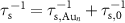 with
with  . In this manner, the cluster contribution to the spin scattering can be distinguished from the virgin scatterers. The result of the fitting are shown as the solid lines and result in a
  cm2 s−1 and
  ps for the Au3 deposition on device A. Au6 on device B produced
  cm2 s−1 and
  ps. These fitted
  's compare perfectly with the spin lifetimes in the virgin state obtained from the Hanle fitting (figure 1(c)). The fitted
  's indicate the size-dependent properties of the two cluster sizes: Au6 is five times more effective as a spin scatterer compared to the Au3 cluster.
In summary, the experiments provide a clear difference between the induced momentum and spin scattering rates per density ( 's) for the two cluster sizes examined. It is found that the Au6 cluster is more effective in momentum scattering by a factor of ten, and in spin scattering with a factor of five compared to the Au3 cluster. Next, to obtain insights in the spin–orbit coupling induced by the cluster, density functional theory simulations are carried out.
5. Density functional theory simulations
In addition to the experiments, first-principles calculations were performed based on density functional theory using the Vienna ab inito simulation package (VASP) with plane wave basis sets [54–57]. First, the most stable geometrical configuration for the graphene-Aun
( 6) system was searched by relaxing the cluster in different orientations and at different adsorption sites on the graphene plane. It is found that the triangular Au3 cluster prefers to adsorb on a C–C bridge position with C-Au bond lengths between the two nearest C atoms 2.25 Å and 2.5 Å. The triangular Au6 cluster prefers a configuration parallel to the graphene plane. The stable geometry of the Au6 cluster is adsorbed 3.5 Å above the graphene plane (see figure 4, panels (c) and (f)). The binding energy of Au3 cluster on graphene is estimated to be −1.57 eV, while that of Au6 cluster is −2.25 eV. These computational results indeed show the position of the bond is different for both cluster sizes. Details on these calculations can be found in the supplementary information (SI section 5).

Figure 4. Au valence orbital projected band structure of Au3/graphene (a) and Au6/graphene (d) without spin–orbit coupling, Fermi level adjusted to 0 eV. The size of the red dots are equivalent to the weighted contribution of Au s and d orbital to the band structure. Panels (b) and (e) corresponds to the computed band structure with spin-orbit interaction for Au3/graphene and Au6/graphene in the vicinity of the Dirac point (full band structure is provided in the supplementary information, section 6). The arrows indicate the intra-band splitting, along which the energy difference between band lines is computed. Panel (c) displays the relaxed structure for Au3/graphene (side view) and panel (f) for Au6/graphene (top view).
Download figure:
Standard image High-resolution imageFigures 4(a) and (d) present the band structures without spin-orbit interactions using a  graphene supercell with 50 carbon atoms (
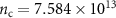 cm−2) and one adsorbed Au3 and Au6 cluster, respectively. It can be seen that the valence Au 6s orbitals of the Au3 cluster are energetically close to the Fermi level and strongly hybridize with the C
  orbital. Furthermore, there is a band opening at Dirac point in graphene-Au3 system. Strong orbital hybridization could be the reason for this gap opening. Taking into account the cluster density in this simulation, the shift of the Dirac point with respect to the Fermi level corresponds to a cluster doping efficiency of ε = 0.062 e/cluster. For Au6 clusters on the other hand, the Au valence orbitals are far from the Fermi level (panel (d) of figure 4). Here, it can be seen that the Au6 cluster does not affect the Dirac cone by much near the Fermi level. Moreover, Au6 adsorption does not shift the Fermi level with respect to the Dirac cone and therefore the Au6 shows a negligible doping efficiency.
The experimental doping efficiencies are not reflected in the DFT calculations. Possible reasons for this mismatch could be due to (a part of) the clusters having a different geometry than what is considered in the DFT simulations, leading to a different interaction and doping efficiency, potentially mediated by the presence of defects/residues on graphene interacting with the cluster. Furthermore, we should keep in mind that we are simulating a free-standing perfect graphene layer interacting with Aun clusters, which may be different from the transferred graphene layer on the Si/SiO2 substrates.
Panels (b) and (e) present closer views at the Dirac cone, in this case including spin-orbit interactions, for adsorbed Au3 and Au6 clusters, respectively. Spin–orbit coupling lifts the degeneracy of spin states and causes band splitting. In graphene spin-orbit interaction opens up a gap in the Dirac cone. Weeks et al studied this SO induced gap for indium and thallium adatom coverage on graphene [18]. However, in the present work there is strong orbital hybridization between graphene and Au valence orbital, opening up a gap even in the absence of SO coupling. Marchenko et al observed a strong enhancement in the SO splitting for graphene covered by a graphene monolayer due to hybridization with Au 5d state [58]. They also observed a splitting of the Dirac cone of a few meV when the graphene sublattice is in top position with respect to the gold monolayer and estimated the SO splitting in the vicinity of the Dirac point along the band line. Marchenko et al estimated the SO splitting by calculating the absolute values of energy difference between band lines along valence band [59]. Therefore, to study and distinguish the SO induced splitting from orbital hybridization, intra-band splitting is measured along the band line away from the Dirac point ( and
and  ) as indicated by the arrows in panels (b) and (e).
The strength of the induced spin–orbit coupling with varying cluster density is studied by performing simulations on different sizes of graphene supercells ( ,
,  ,
,  and
and  carbon atoms supercells) containing one Au3 or Au6 adsorbed cluster. The estimated SOC strength from the computed band structures are shown in figure 5, evaluated in a range of −0.1 eV to −0.6 eV below the Dirac point. The errorbars present the range in SOC in this energy interval. The SOC induced intra-band splitting is in the range of 4–13 meV for Au3 and 2–5 meV for Au6. So, also for the SOC a cluster size dependence is observed with Au3 inducing a larger SOC. A SOC of the same order of magnitude (
 meV) has been reported for Rashba SOC in graphene in contact with a full layer of Au atoms [58, 60]. Theoretical predictions also yield similar results for impurities on graphene [10]. Next, the DFT simulations are compared to the experimental observations.

Figure 5. Averaged spin-orbit induced intra-band splitting for different cluster densities (i.e. different supercell sizes) for both Au3 and Au6.
Download figure:
Standard image High-resolution image
6. Discussion
In order to compare the DFT results to the experiments, a specific spin scattering mechanism needs to be considered in order to extract a SOC energy from the experimentally obtained scattering lifetimes ( and
and  ). In both devices, the spin lifetime decreases as the momentum scattering time is reduced, indicating an Elliot–Yafet (EY)-like [61, 62] spin scattering induced by the gold clusters. The spin scattering rate in the EY mechanism is
  . Note that the Fermi level
  eV is constant in the experiment since the charge carrier density was fixed at
  holes cm−2 by tuning the back-gate voltage. In order to extract the SOC induced by the clusters, the Matthiessen's rule is applied as before to exclude the virgin state's contribution. Therefore,
 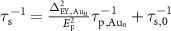 , with
  the induced SOC by the gold cluster assuming the EY mechanism as the dominant spin relaxation mechanism and
  the spin lifetime in the virgin state. Rewriting this equation results in an EY SOC induced by the gold clusters

Using the fitted  and
and  , the
, the  is found to be
  meV and
  meV for Au3 and Au6, respectively. As the EY SOC is related to a spin scattering probability at each momentum scattering event, a cluster density independent
  is compatible with the EY theory [63]. Both the order of magnitude and the relative
  strength of the Au3 and Au6 systems are consistent with the SOC extracted from the density functional theory simulations (see figure 5), which did not show a clear trend with the cluster density, further supporting the EY scattering mechanism.
In summary, a consistent cluster size dependence of the SOC is seen in experiment and DFT simulations. The SOC differs a factor of 2–3 in the simulations and about  in the experiments between Au3 and Au6 decorated graphene, with Au3 inducing the largest value.
7. Conclusion
This work demonstrates the manipulation of spin currents using adsorbed size-selected Au clusters in a graphene spin valve. It was found that Au6 clusters adsorbed on graphene are more effective momentum and spin scattering centres per density compared to Au3 clusters. Guided by ab initio simulations, similar SOC values were found in the simulations assuming that Aun
clusters ( 6) scatter the diffusing spins through the Elliot–Yafet mechanism. Moreover, it is found that the adsorbed Au3 cluster induces a stronger spin–orbit coupling in graphene than the adsorbed Au6 cluster. This indicates the importance of the exact positioning of the adparticle on the graphene lattice as well as the strong size-dependent properties of the cluster. This approach not only provides insight into the spin relaxation mechanism, but opens possibilities to investigate the robust quantum Hall state and the (i)SHE towards spintronic applications.
Acknowledgments
This research has been supported by the Research Foundation-Flanders (FWO project G.0D56.19N) and by the KU Leuven Internal Research Fund C14/17/080.
Data availability statement
The data that support the findings of this study are available upon reasonable request from the authors.