
Abstract
We demonstrate that thicker layers can be achieved in gallium nitride (GaN) epitaxy by using a patterned silicon (Si) substrate compared to a planar Si substrate. GaN films were grown by metalorganic vapour-phase epitaxy on 6-inch Si (111) substrates patterned with arrays of squares with various corner shapes, height and lateral dimensions. Stress spatial distributions in the GaN pattern units were mapped out using confocal Raman spectroscopy. It was found that the corner shapes have an effect on the uniformity of the stress distribution. Patterns with round corners were found to have more uniform stress distribution than those with sharp corners. The largest crack-free square size for a 1.5 μm thick GaN film is 500 × 500 μm2.
Export citation and abstract BibTeX RIS

Original content from this work may be used under the terms of the Creative Commons Attribution 4.0 licence. Any further distribution of this work must maintain attribution to the author(s) and the title of the work, journal citation and DOI.
1. Introduction
The continuous improvement of III-Nitrides growth processes opens a new possibility for future power devices. However, the growth of thick gallium nitride (GaN) on silicon (Si) substrates remains a problem for III-V semiconductor technology. The large mismatch in the thermal expansion coefficients between GaN and Si (55%) lead to high crack density on GaN surface [1, 2]. The GaN layer grown by metalorganic vapour-phase epitaxy (MOVPE) results in tensile stresses on Si wafer and in compressive stresses on sapphire [3]. For nearly two decades, AlN transition layer or thick AlxGa1−xN grading between Si and GaN was only method in order to suppress the formation of cracks in grown films [4]. By inserting different AlxGa1−xN interlayers, compressive stress is introduced to compensate the tensile stress produced during the cooling process to eliminate surface cracking. The growth on silicon-on-insulator (SOI) substrate allows using significantly thinner AlGaN buffer layer compared with the growth on bulk Si [5], however build-up of stresses during epitaxy results in GaN cracking at thicknesses exceeding 1μm. Recently, the thin AlN transition layer grown on Si by plasma-enhanced atomic layer deposition (PEALD) has been demonstrated [6]. Despite fact, that layer was polycrystalline, PEALD remains promising low-cost method for the formation of nucleation layers.
Selective area growth (SAG) has been proposed to reduce build-up of stress during GaN epitaxy. A SAG method was applied to the GaN growth on Si, where Si substrate is covered by a SiO2 or SiN patterned mask in order to suppress the formation of GaN cracks [7]. Subsequently, a non-continuous GaN film can be directly grown on these Si substrates. For window sizes of (0.1–0.2) mm × (0.1–0.2) mm, 1.5 μm thick GaN films free from cracks have been achieved [8, 9]. So far, SAGs have extensively used rectangular growth patterns where the stresses peak at the pattern corners and it is at these corners where the crack in the GaN layers nucleates [9–11]. In a recent work, 19μm thick crack-free GaN layers on Si has been reported [12], where SAG was performed for circular patterns with 350μm diameter. As their thermal stress simulations showed, the corner stress is significantly reduced when more corners were added to the pattern and is lowest for a circular interface. Although the combination of these two approaches, the AlN transition layers and SAG, result in improved material quality in the overgrown regions, the size and shape of patterns are still limited and the method has not been demonstrated on large area substrates. Furthermore, they require a re-growth procedure in which the grown sample is taken out of the reactor for the deposition and patterning of a masking layer, or for etching the seed layer, and then inserted back into reactor to complete the growth.
So far, patterned Si wafers are mainly utilized for semi-polar GaN growth [13]. However, in [10], the effect of pattern size on crack density was studied for Ga-polar GaN. For this goal, the GaN layer was grown on patterns of different sizes (5–100 μm) fabricated using reactive ion etching (RIE) on (111) Si wafer. The layer is grown under conditions similar to those of an unpatterned layer and enables an analysis of the effect of lateral dimension changes on the layer properties. The trenches between mesas were 0.5–0.6 μm deep and 2–4 μm wide. It was shown that crack-free material of thickness ∼0.7 μm, can be grown on square patterns smaller than 14.0 ± 0.3 μm size.
In this article, the effects of using a patterned 6-inch Si (111) substrate for metalorganic vapour-phase epitaxy (MOVPE) GaN growth are investigated. We present a systematic study on the effect of patterned Si substrate parameters on epitaxial growth and resulting layer quality. Moreover, an extended study of a method presented in [10] is also given. By the variation of different size parameters, trench depth and corner shapes we were able to reach 1.5 μm crack-free thick GaN on patterned 6-inch Si wafer. The nature of stress spatial distributions in the GaN pattern units were extensively studied by the post-growth Raman scattering studies.
2. Experiment
2.1. Patterned Si wafers
Three different 6-inch Si (111) substrates for GaN growth were investigated: a bulk silicon substrate (non-patterned) and patterned silicon substrate with 10 μm (sample A) or 40 μm (samples B) deep trenches between mesas. Mesas were square shape with sizes of L: 500, 1500, 3000, 5000 μm, and trenches between mesas, W: 20, 50, 150 μm as shown on a figure 1. All substrates were p-type silicon (111) with total thickness 1000 ± 25 μm.

Figure 1. Schematic picture of 6-inch wafer and square pattern mesas with different sizes L: 500, 1500, 3000, 5000 μm and trenches between mesas, W: 20, 50, 150 μm. All squares have sharp corners except for the zones 2, 4 and 8, where they have round corners.
Download figure:
Standard image High-resolution imageIn order to determine effect of corner stresses, zones 2, 4 and 8 (figure 1) had round shape corners, zones 1, 3 and 5–7—sharp corners, the difference shown on figure 2. The substrates were manufactured by Okmetic Oyj.

Figure 2. Round shape (a) and sharp (b) corners of patterned wafers.
Download figure:
Standard image High-resolution image2.2. MOVPE growth
GaN (0001) layers were grown on Si wafers using the standard step graded AlxGa1−xN and AlN approach by the metalorganic vapour-phase epitaxy (MOVPE). The reactor had a 1 × 6-inch close coupled showerhead configuration. Thimethylaluminium (TMAl), thimethylgallium (TMGa) and ammonia (NH3) were used as precursors for aluminium, gallium and nitrogen, respectively. Hydrogen was used as the carrier gas, more details can be found in [5].
Figure 3 presents cross-sectional SEM image of the structures grown on non-patterned Si substrates. The growth process was started by in-situ annealing to remove the surface native oxide. After annealing, a 300 nm AlN buffer was deposited. The buffer consists of low temperature and high temperature AlN grown at 980 °C and 1085 °C nominal substrate surface temperature, respectively. Next, a step graded AlxGa1−xN buffer was grown at 1060 °C with three different compositions. These were 260 nm of Al80Ga20N, 280 nm of Al50Ga50N and 470 nm of Al20Ga80N. Finally, 900 nm of GaN was grown at 1040 °C. The sample parameters are listed in table 1.
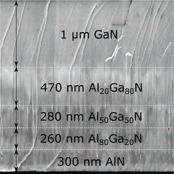
Figure 3. Cross-sectional SEM-image of the epitaxial layers on non-patterned Si.
Download figure:
Standard image High-resolution imageTable 1. Fabricated sample structures.
| Sample | non-patterned Si | A | B |
|---|---|---|---|
| Si (μm) | 1000 | 1000 | 1000 |
| AlN (nm) | 300 | 300 | 300 |
| Al80Ga20N (nm) | 260 | 260 | 600 |
| Al50Ga50N (nm) | 280 | 280 | 600 |
| Al20Ga80N (nm) | 470 | 470 | 500 |
| GaNa (nm) | 600 | 600 | 1200 |
| GaNb (nm) | 300 | 300 | 320 |
The reactor pressure during growth was 100 mbar, except for the last GaN which was grown under 400 mbar pressure. The higher growth pressure increases the crystalline quality of GaN while material grown at 100 mbar pressure has a higher carbon concentration and forms a semi-insulating layer [14]. This type of semi-insulating layer is typically used for device insulation, for example, in GaN high electron mobility transistors (HEMTs). Device layers, such as HEMT or light emitting diode (LED), could then be grown on these epitaxial templates.
An optical in-situ measurement system was used to assess the growth rate and wafer surface temperature profile. A more detailed measuring mechanism description is explained in detail in [5]. Besides an optical in-situ measurements, the thickness measurements were verified with cross-sectional scanning electron microscope (SEM). Moreover, a behaviour of crack distribution was studied by SEM. The surface roughness of the GaN layers was determined by atomic force microscopy (AFM).
2.3. Local stress analysis via confocal Raman spectroscopy
Confocal Raman spectroscopy is a nondestructive and sensitive optical method for quantitative characterization of stress distribution in GaN layers via observing Raman peak shifts [12, 15–17]. Modern Raman tools operate close to the optical diffraction limit and are capable of detecting the local stresses with lateral spatial resolution of only 0.5 μm [18]. However, due to the tiny magnitude of Raman peak shifts, it is noteworthy that the Raman 1-D, 2-D and 3-D measurements are easily influenced by various potential error sources that can distort the scan results if not accounted for [19–21]. For accurate measurements, a laser induced heating and stress should be considered due to their effect on the Raman peak shift [22]. Another major error source can be a lack of proper spectrometer calibration, often affected by the environment in real time, because it is used to linearize the spectral axis and thus correct the Raman peak shifts [17]. In order to estimate absolute stress values, both of these effects were accounted for in this work. The essential point to remember is that the collected spectra are to be interpreted with care due to the fact that a multi-layered high refractive index film is being measured as depicted in figure 3. In other words, although the laser beam was carefully focused on the air-GaN interface, its collection volume extends through all the grown layers and results in a weighted sum of each layer spectrum.
To evaluate the local residual stress differences in the grown GaN layers, a confocal Raman microscope, WITec alpha300 RA+ was used in the backscattering configuration to estimate the absolute biaxial stress, σxx from the Raman peak position, ω of GaN's main optical phonon mode,  . When the biaxial stress component is dominating, their linear relationship can be written as
  , where, in case of the Raman peak
  568 rel. cm−1 is a still-debated stress-free value [12, 15] and K = 4.2 cm−1 GPa−1 is an experimentally measured phonon deformation potential [12, 23]. The Raman scattering was excited by a 488nm wavelength laser with 10 mW power, focused through an intermediate magnification/numerical aperture×20/0.4 dry objective lens. A MATLAB toolbox wit_io was used to boost the data analysis [24].
3. Results and discussion
3.1. 900 nm thick GaN on non-patterned 6-inch Si substrate
As a practical example of biaxial stress analysis, the GaN layer grown on non-patterned Si substrate was line scanned ∼1 cm from its center and edge, as demonstrated in figure 4. The center and the edge regions of the wafer were found to be spatially uniform with tensile biaxial stresses of σxx = 468 ± 33 MPa and σxx = 528 ± 41 MPa, respectively. Here plus-minus sign represents standard deviation from the mean value. Averaged tensile biaxial stress is then found to be σxx = 498 ± 47 MPa (total of 102 data points from total of 2 line scans). Observed anomalous deviations from the mean in figure 4 (b)–(c) and (f)–(g) are attributed to some local changes within the multilayer film structure, for instance, to a local defect, but detailed analysis is beyond the scope of this work. The top layer surface uniformity was verified by AFM measurement with a root-mean-square (RMS) roughness of 1.46 nm for 10 × 10 μm image scan.
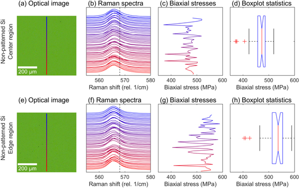
Figure 4. Row-by-row comparison of biaxial stresses in the center (the top row) and the edge (the bottom row) regions for the non-patterned Si sample. The columns are as follows: (a) and (e) show the 600 μm vertical line scan positions in the optical images with green tint due to a 488 nm laser notch filter. (b) and (f) give a cascaded representation of the  Raman peaks for total of 51 spectra. Here the change in color is equivalent to the change in position within the line scan. Dashed vertical line marks the stress-free
  Raman shift at ω0=568 rel. cm−1. (c) and (g) display the tensile biaxial stresses calculated from the Lorentz-fitted
  Raman peak position. (d) and (h) summarize the biaxial stress statistics with use of notched box plots. Here the median value is shown by the red vertical line, the 95% confidence interval by the triangle notch, the interquartile range by the blue box ends, the statistical data limits by the black vertical whiskers and the outliers by the red plus signs.
Download figure:
Standard image High-resolution imageThe obtained biaxial stresses are not high and are comparable to the previous research [12]. The small stress difference could be explained by the different temperature in the center and edge of the substrate during GaN growth.
In order to account for the instrument spectral axis nonlinearity, a highly spectrally stable bulk ammonothermally grown GaN reference sample spectrum was also taken with each measurement. The reference sample spectrum was once meticulously linearized using dozens of neon atomic lines, explained in detail in this [17]. Each collected spectra was then Raman shifted together with the corresponding reference spectrum in a way that the peak of interest, the main Raman peak of GaN,  recovers its absolute position. It is noted here that possible but small laser-induced heating effect to the peak positions was assumed to be sufficiently equivalent for each sample and thus is handled by the previously described methodology.
3.2. 900 nm thick GaN on patterned 6-inch Si substrate
The same MOVPE process recipe used for the GaN growth on non-patterned Si was then utilized for a patterned Si wafer, denoted as Sample A. Figure 5 presents emissivity-corrected in-situ substrate surface temperature and 633 nm wavelength reflectance during a growth run on (a) non-patterned Si and (b) patterned Si substrate (Sample A). It can be seen that the patterned substrate does not significantly alter the growth. The growth rates are 0.5 μm h−1, 1.1 μm h−1, and 2.3 μm h−1 for AlN, AlGaN and GaN layers, respectively for the growth on both substrates. The similar growth rate of high pressure GaN in both cases (1.2 μm h−1) shows that epitaxy is not affected by substrate patterning. Nevertheless, the amplitude is slightly smaller on a patterned substrate due to the fact that measured point covers both the mesa and trench. The effect of mild layer degradation during AlGaN buffer deposition (5000–9000 s) is due to surface roughening, this can be optimized in future.

Figure 5. In-situ substrate surface temperature and reflectance data during growth on (a) non-patterned Si and (b) patterned Si. For patterned substrates, the measurement spot covers both the mesa and trench.
Download figure:
Standard image High-resolution imageFigure 6 demonstrates microscope top view images of grown GaN layers on 20/500 μm mesas. It can be seen that GaN grown on both mesas with sharp corners (a) and round corners (b) is crack-free. However, the GaN grown in the areas outside mesa patterns are cracked from trenches with sharp corners, as is shown by arrows in figure 6(c). For round corners in (d), they remained crack-free. In fact, sharp corner trenches generate GaN cracks between mesas while round corner trenches prevent GaN from cracks. The high-resolution stitching microscope image of the whole crack-free pattern is demonstrated in figure 7.

Figure 6. Microscope images of crack-free GaN on 20/500 μm mesas with (a) sharp corners and (b) round corners of sample A. Optical microscope images of GaN grown on the edge of size W = 20 (μm) trench with (c) sharp corners and (d) round corners. Arrows indicate cracks in (c) between mesa patterns.
Download figure:
Standard image High-resolution image
Figure 7. Microscope image of the crack-free 900 nm thick GaN grown in pattern with 20/500 μm sharp corner mesas of sample A.
Download figure:
Standard image High-resolution imageFigure 8 shows a cross-section edge of the 20/1500 μm square patterned zone of Sample A. The thickness difference of the grown layer in mesa and trench areas is mostly due to a higher growth rate and earlier coalescence of GaN crystallites on top of the mesas. The GaN growth direction in flat mesas and trenches bears a similarity to a standard c-plane (0001) growth on (111) Si. The growth direction in side walls is supposedly (11-20) a-plane, but proof of this requires additional x-ray diffraction measurements.

Figure 8. Cross-sectional SEM image of the 20/1500 μm mesa and trench (Sample A).
Download figure:
Standard image High-resolution imageFigure 9 displays a GaN stress distribution comparison between the sharp (zone 3, figure 1) and round (zone 8, figure 1) cornered mesas. The perceptually uniform color map of matplotlib [25] was chosen for representing the stress maps to aid in the visual inspection in the least biased way. This allows us to see in figure 9 that GaN in the round corner mesa (b) is slightly more tensile stressed than in the sharp corner mesa (a). The cross-sections (figure 9(e)) indicate to an excellent stress distribution uniformity in vertical (V) and horizontal directions (H). In contrast to previous reports on the circle shaped mesas, where compressive strain is maximum at the center and relaxes towards all the edges [12, 16], here stresses distribute uniformly for the whole square mesa surface. However, the slight asymmetry in figure 9(e) could be caused by an unintentional artifact of accumulated instrumental errors [17], since biaxial stress distributions in figures 9(a) and (b) tend their highest values towards the bottom-right corners. From the comparison of figures 9(c) and (d) it is easy to note that the round corners seem to alleviate the stress more quickly than the sharp corners. The same effect is presented in the cross-section measurements (f). Here semi-transparent thick trend lines are the 1st order polynomial fit lines and were added to demonstrate that the round corner mesa reaches the stress equilibrium slightly faster than that of the sharp corner mesa, also seen in (e).

Figure 9. Comparison of biaxial stress distribution by Raman mapping for the sharp (a) and round (b) corner 20/500 μm mesas in sample A with the same perceptually uniform color scaling. Cross-section (e) plots the normalized biaxial stress from red (a) and blue (b) rectangles with respect to the mesa maximum. (c) and (d) show the top-right corners of each mesa via a high resolution image scan. Cross-section (f) indicate biaxial stress values from red (c) and blue (d) lines normalized with respect to the mesa maximum.
Download figure:
Standard image High-resolution imageThe line-averaged tensile biaxial stresses calculated in table 2 supports Raman map results. Based on table 2, patterned Si substrate has some effect on the GaN stress values. GaN on non-patterned Si substrate has slightly lower tensile biaxial stresses. This is probably due to GaN thickness difference between samples. The GaN layer in round corner mesas is slightly more stressed than in sharp ones. This is probably due to stress difference between the edge and center of wafer similarly to non-patterned Si.
Table 2. Comparison of σxx biaxial stress averages in GaN layer grown on the 6-inch non-patterned and patterned Si substrates (Sample A). Each value was calculated from two Raman line scans.
| Sample | GaN thickness (nm) | Mesa | Data size | σxx (MPa) |
|---|---|---|---|---|
| A | 875 ± 25 | a20/500 μm | 72 | 547 ± 24 |
| A | 875 ± 25 | b20/500 μm | 79 | 618 ± 34 |
| non-patterned Si | 860 ± 47 | — | 102 | 498 ± 47 |
3.3. 1.5 μm thick GaN on patterned 6-inch Si substrate
The effect of substrate patterning on thicker GaN films was investigated with sample B, where time for Al80Ga20N, Al50Ga50N and GaNa scaled by factors of 2, while other layers kept similar to sample A. For sample B a patterned substrate with trench depth of 40 μm was used. In-situ reflectance data of sample B is shown in figure 10. As can be seen, reflectivity trends same behavior with sample A. A small decrease in reflectance amplitude, most probably due to a different trenches depth in measurement area, otherwise reflectivity is similar to the sample A/non-patterned Si. Nevertheless, the slight drop in the reflectivity average during AlxGa1−xN buffer growth indicates to increasing surface roughness, that require further optimization.

Figure 10. In-situ substrate surface temperature and reflectance data during growth on sample B.
Download figure:
Standard image High-resolution imageFigure 11 shows microscope image of Sample B 20/500 μm mesa surface, no cracks are seen. The total thickness of grown layers is supported by the cross-sectional SEM image (figure 11 (b)). In case of L ≥3000 μm, the GaN grown on the mesa often exhibited cracks. This effect of mesa size is probably due to a substrate bowing and cooling effects [26]. Although the growth process was developed for non-patterned Si substrates, it could be further optimized for growth on patterned wafers. As a result, with simply increasing growth time its possible to obtain crack-free thick GaN on patterned substrate.

Figure 11. (a) Top view of 1.5 μm crack-free GaN grown on patterned Si substrate with 20/500 μm mesas (Sample B), (b) cross-section of grown crack-free GaN layer in 20/500 μm mesas of sample E.
Download figure:
Standard image High-resolution imageOne of the crack-free GaN 20/500 μm mesas was 2-D scanned with confocal Raman spectroscope to show its stress distribution for visual comparison purposes as illustrated in figure 12. Averaged tensile biaxial stress is then found to be σxx = 761 ± 24 MPa (total of 65 data points from total of 2 line scans) which is more tensile stressed than sample A, but still has no cracks. In contrast to the sample A (Figure 9(a)), where stresses are distributed more evenly on the mesa surface, here the stress maximum is concentrated in the center of the mesa (figure 12 (a)). The color scaling was set same in all figures for comparison purposes. The cross-sections for normalized biaxial stress values (Figure 12 (b)) also demonstrates reaching the equilibrium point significantly slower than sample A (figure 9(e)). The effect of higher GaN strain and different stress distribution is probably due to the larger contribution of the low pressure GaNa to the summarizing GaN layer. For further growth optimizations, the thickness ratio of GaNa/GaNb should be considered.

Figure 12. Biaxial stress analysis for the sharp corner 20/500 μm mesa in sample B: (a) shows stress map, with rectangles in red mark the averaging cross-sections, plotted in (b). For mesa-to-mesa comparison purposes the cross-sections were normalized with respect to the mesa maximum. Dashed vertical lines reveal the mesa edges.
Download figure:
Standard image High-resolution image
4. Conclusions
Growth of 1.5 μm thick crack-free GaN on patterned 6-inch Si substrate was demonstrated. Crack-free growth was obtained on 20/500 μm size mesas, larger mesas exhibited cracks. Patterned Si substrates open a wide range of possibilities for various device applications. Therefore, these type of GaN templates on patterned Si could be used for LED or HEMT fabrication. Moreover, from fabrication point of view, trenches could be used for device dicing.
Confocal Raman spectroscopy measurements allowed to calculate σxx biaxial stresses of GaN in patterns. Results show that patterned Si substrate does not significantly alter the growth. In addition to that, the high resolution Raman scan reveals that further stress control is possible by controlling the corner shape of mesas.