

Abstract
This paper presents the development of planar zinc (Zn) resistor–capacitor (RC) filters from a single printed layer that are both printed and treated at room temperature. The fabrication process involves screen printing the resistor, capacitor and interconnects in a single patterned layer on kraft paper substrates using a Zn microparticle ink. In order to form a distinct resistor and capacitor in the patterned structure, reactive inkjet printing (RIJ) was performed to selectively dispense acetic acid on the RC filter pattern to achieve regions with highly contrasting resistance. The required high degree of spatial contrast was achieved using the positional control of the inkjet printer combined with the number of print passes and drop spacing used to dispense the acetic acid droplets. X-ray diffraction and scanning electron microscopy showed the crystal structure and grain size of Zn microparticles remained unchanged with increasing acetic acid exposure while the prominence of cold-welding increased with increasing exposure. Zn-based RC filters sharing a common set of dimensions but with a wide range of corner frequencies were successfully fabricated using this process. For a fixed filter geometry, the corner frequencies could be tuned from ∼7 kHz to ∼1 MHz as the number of print passes used to form the resistor increased in a stepwise manner. To the best of our knowledge, this is the first room temperature printing process to produce side-by-side resistors and conductors from the same printed layer and the first printing process of any type to produce RC filters with such a wide range of corner frequencies.
Export citation and abstract BibTeX RIS

Original content from this work may be used under the terms of the Creative Commons Attribution 4.0 license. Any further distribution of this work must maintain attribution to the author(s) and the title of the work, journal citation and DOI.
1. Introduction
Inkjet printing leads all additive manufacturing methods in the production of high quality electrical conductors [1–3] interconnects [4, 5] planar antennas [6–8], RFID systems [9–11], sensors/transducers [12–14] and a host of other electronic devices that utilize metals as the principal functional material. As such, development of printing processes has principally focused on achieving metallic structures with the highest possible electrical conductivity. Unfortunately, the number of processes designed specifically for the printing of high quality resistors is significantly lacking. Resistors are typically integrated into inkjet-printed circuits using the sophisticated bonding techniques associated with surface mount devices (SMDs) [15]. The integration of mechanically rigid SMDs hinders the mechanical flexibility of printed electronics and complicates the fabrication process. Printed resistors are typically fabricated using resistive carbon inks [16]. A wide range of resistances can be achieved by tuning the conductor/filler concentration [17] or by varying the geometry of the printed resistor (i.e. length, width, and thickness) [18]. Alternatively, resistance can be tuned via adjustments in the printing or treatment processes. For example, resistors have been printed using a silver nitrate-based precursor ink and an ascorbic acid-based reducing agent by printing the precursor ink and reducing agent separately in different sequences to achieve resistivities that vary by over four orders of magnitude [19]. Likewise, resistors have been formed using plasma reduction of a silver nitrate precursor ink using plasma treatment duration and plasma power to vary the resistivity by over six orders of magnitude [20]. To the best of our knowledge, a printing-only process capable of producing both high resistance and low resistance structures side-by-side in a single printed layer has yet to be developed.
The resistor–capacitor (RC) filter is a simple electronic device that utilizes both low resistance and high resistance circuit elements. In addition to its utility in a wide variety of electronic circuits, the RC filter is a convenient device to assess the efficacy and versatility of processes designed specifically to produce printed resistors. Several approaches have been used to fabricate RC filters by printing. Chen et al printed RC filters constructed of PEDOT:PSS conducting polymers [21]. The resistors and capacitors in these filters were fabricated in two distinct printed layers using two PEDOT:PSS inks of different chemical compositions to achieve variations in electrical conductivity. Moreover, the process required a curing step at 50 °C. Cao et al printed RC filters using two distinctly different inks: a PEDOT:PSS ink to form the resistor and a Ag nanoparticle ink to form the capacitor [22]. Their process required thermal treatment at 100 °C after printing to achieve the desired electrical properties. Sinar et al printed graphene-based RC filters using graphene-carboxymethyl cellulose inks. These structures required a thermal step at 320 °C after printing in order to decompose the ink [23].
As the preceding examples indicate, the fabrication of printed RC filters is challenging because the resistor and capacitor structures must either be fabricated using inks of different materials or using inks that require thermal processing steps to achieve distinct resistivities. Except under extreme conditions, it is not currently possible to fabricate the two components in a single printed layer, in particular on temperature sensitive substrates. The ideal process would utilize a non-thermal post-printing step with spatial control of electrical resistivity, thus enabling the fabrication of capacitors and interconnects alongside resistors in a single printed layer. Additionally, this process would enable the fabrication of structures that exhibit a wide range of electrical resistivity by varying an easy-to-control set of process parameters during the post printing step. The ideal process would be compatible with a wide range of temperature-sensitive substrates that are currently attractive for printed electronics but are incompatible with conventional inkjet printing techniques, which typically require annealing at temperatures above 100 °C. Inspiration for the work described in this paper comes from a previous study where we used low pressure argon (Ar) plasma to fabricate RC filters from a single inkjet printed Ag layer [24]. In that case, plasma was selectively applied to the printed structure to control the resistance of the capacitor and resistor. This process was effective in fabricating low-pass RC filters with corner frequencies ranging from 544 kHz to 3.6 MHz, but suffered from two process-related limitations: (1) the plasma lacked any degree of spatial control, requiring the use of a shadow mask to protect the resistors from excessive plasma exposure and (2) plasma bombardment resulted in substrate temperatures between ∼60 °C and ∼90 °C depending on the duration of plasma exposure. To address these limitations, this paper describes the development of a room-temperature printing process to fabricate RC filters from a single printed Zn layer using reactive inkjet printing (RIJ) to selectively dispense an acetic acid reducing agent. The work detailed in this paper leverages our previous work to develop low resistance Zn-based conductors using an acetic acid oxide etchant to form the conductors from Zn microparticle inks [25]. In that work, RIJ was used to selectively dispense the acetic acid in order to minimize damage to the patterned structure due to excessive exposure to the acid. The work reported herein builds upon that study by extending the RIJ process to resistor-based devices like RC filters.
2. Experimental methods
2.1. Printing details
Following the procedures described in our previous study to develop highly conductive Zn structures [25], a screen-printable Zn ink containing Zn powder was prepared as follows. First, polyvinylpyrrolidone (PVP) powder (Sigma Aldrich) was mixed with N-methyl-2-pyrrolidone (NMP) (Sigma Aldrich) in a glass vial using a PVP:NMP ratio of 1:5 w/w. Specifically, 1 g of PVP powder was mixed with 5 g of NMP. The PVP/NMP mixture was then stirred for 48 h on a 60 °C hotplate. Then, 30 g of Zn powder (1–5 μm particle size, Goodfellow Co.) was added to the PVP/NMP solution. Following this, the mixture was loaded onto a vortex mixer (Genie SI-0236) operating at 3200 rpm for 3–5 min to be fully dispersed. To further improve dissolution, a spatula was used to manually stir the Zn:PVP/NMP mixture. A detailed description of the ink and its properties are presented elsewhere [25].
A screen mesh with the desired RC filter patterns was designed in house and fabricated by a commercial vendor. A calendared stainless-steel mesh (325 Cal, 0.0011 in wire diameter, 0.002 in wire opening, SEFAR Inc.) was used to make linear resistors and RC filter devices. Samples were printed at room temperature on glass, silicon (Si) and kraft paper substrates. The average resistance for the as-printed samples exceeded the range of a Keithley 2000 multimeter (> 100 MΩ).
RIJ was then performed using an inkjet printer to control the deposition of the acetic acid chemical deoxidizing agent on the screen-printed Zn patterns. A Fujifilm Dimatix DMP3000 printer with 16 piezoelectric nozzles (DMC-11610) was used to print the acetic acid (CH3COOH). The acetic acid was diluted in deionized water (H2O) (CH3COOH: H2O = 1:10), after which 10 mL of this solution was loaded into the printer cartridge. The nozzle actuation voltage was set at 18 V. The drop spacing of the printer was set at 15, 25 and 35 μm, depending on the local Zn region to be deoxidized: the resistor pattern or the capacitor pattern. The platen temperature of the printer was set at room temperature.
2.2. Electrical testing
A Keithley 2000 Multimeter was used to measure the resistance of Zn samples after the RIJ step. The capacitance was measured using an LCR meter (GW-INSTEK LCR-821). Kelvin clips were connected to each interdigitated capacitor following each inkjet printing pass. To study the frequency response of the Zn RC filters, a 4-channel oscilloscope (Keysight InfiniiVision MSOX3024-200 MHz bandwidth) was used to generate a Bode plot of the RC filter and also the transient response of the RC integrator in the time domain. Each RC filter sample was connected to the Keysight oscilloscope, which had a built-in signal generator. A sinusoidal wave with 2.5 Vpp was generated and the frequency was swept from 10 Hz to 20 MHz. The oscilloscope automatically generated the Bode plot by calculating 20 log (Vo/Vi ) in real-time.
2.3. XRD and SEM analysis
The crystallinity of the printed Zn features was determined by X-ray diffraction (XRD) using a Bruker AXS system. Samples for XRD analysis were printed on glass slides to suppress unwanted background signals. Plan-view and cross-sectional scanning electron microscopy (SEM) was performed using a Thermo Fisher Apreo 2 system to assess the morphology and microstructure of the printed Zn structures. Samples for SEM imaging were printed on Si substrate in order to suppress charging effects and for ease of handling.
3. Results
3.1. Resistance versus print passes
Figure 1 plots the resistance versus number of print passes used during the RIJ step for a set of linear (2 mm × 8 mm) Zn resistors. The drop spacing of the printer was set at 25 μm. Figure 1 shows that the resistance decreases by nearly an order of magnitude from 3108 Ω to 802 Ω between 1 and 4 print passes and again from 802 Ω to 74 Ω from 4 to 8 print passes. This result is consistent with what we found in our previous study for screen printed Zn samples treated with acetic acid under similar conditions [25].
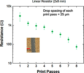
Figure 1. Resistance of rectangular Zn resistors versus the number of acetic acid print passes at 25 µm printer drop spacing.
Download figure:
Standard image High-resolution imageFor comparison purposes, the average resistance for screen printed resistors exposed to acetic acid by conventional pipette-based manual drop casting was also measured. The volume of acetic acid dispensed during the drop casting step was in the sub-milliliter range. The average resistance for the samples treated by drop casting was 14.25 ± 10.63 Ω, which was ∼5x lower than that of samples treated using 8 print passes. The high standard deviation is related to variabilities associated with manual drop casting combined with thickness variations in the screen printed test samples. It should be noted that the estimated total volume of acetic acid dispensed after 8 print passes was ∼64 nL, which is at least 4 orders of magnitude smaller than that dispensed by drop casting.
3.2. Capacitance versus print passes
The capacitance of an interdigitated electrode with 9 fingers was measured as a function of print passes. The drop spacing was set at 15 μm to achieve higher conductivity in the interdigitated structures compared to the Zn resistors described above. Figure 2 shows that the capacitance was independent of print passes at ∼4.2 pF, suggesting that the smaller drop spacing was sufficient to ensure full deoxidation of the Zn ink at least on the surface of the structure.
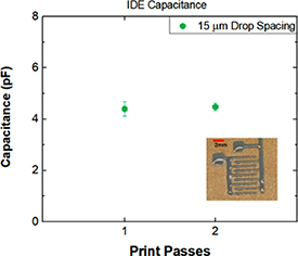
Figure 2. Capacitance versus print passes for a 9 finger interdigitated electrode capacitor.
Download figure:
Standard image High-resolution image3.3. RC filter fabrication and frequency response
The fabrication process for RC filters is illustrated in figure 3. After screen printing the RC filter pattern (figure 3(a)), the sample was dried under ambient conditions for 24 h. Then, the interdigitated electrode-based capacitor and the short interconnect that links the capacitor to the resistor was exposed to acetic acid via the inkjet printer using 2 print passes at a drop spacing of 15 µm (figure 3(b)). Next, the drop spacing of the inkjet printer was set at 35 µm and used to dispense acetic acid on the linear resistor (figure 3(c)). Based on the finding illustrated in figure 1, this step was performed for up to 6 print passes to tailor the resistance of the resistor. Figure 3(d) shows the completed fabrication process, where shading is used to illustrate the position of the capacitor and resistor in the single, planar Zn layer. In this study, five sets of RC filters with each set consisting of six distinct RC filter devices that differ only by the resistance of the resistor were printed using this method.
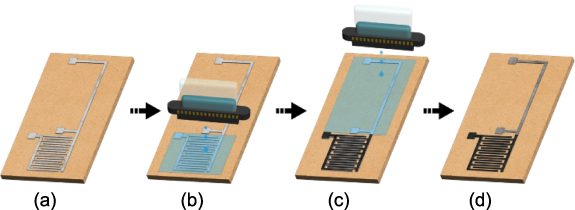
Figure 3. Schematics of Zn-based RC filter fabrication process. (a) As-screen printed RC filter. (b) Dispensing of acetic acid on the capacitor using inkjet printing with 2 print passes at a drop spacing of 15  m. (c) Dispensing of the acetic acid on the resistor using inkjet printing with 1–6 print passes at a drop spacing of 35
  m. (d) Completed fabrication of Zn-based RC filter.
Download figure:
Standard image High-resolution imageFigure 4 is a photograph of a Zn RC filter on a kraft paper substrate after the RIJ steps. The pad dimensions for this device are 2.5 mm × 2.5 mm. The total length of the resistor is nominally 43 mm. The 9-finger capacitor comprises an area of 9 mm × 8 mm inclusive of the interdigitated electrodes. The electrode gap is 0.5 mm. The width of the resistor and connectors are 1 mm while the electrode finger width for the capacitor is 0.5 mm.
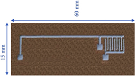
Figure 4. Photograph of a Zn RC filter printed on kraft paper.
Download figure:
Standard image High-resolution imageFigures 5(a) and (b) present the measured Bode magnitude and phase plots of a representative set of RC filters fabricated using the aforementioned technique. The frequency response plots were generated using the MSOX3024 oscilloscope. The corner frequencies of the filters were experimentally determined from the Bode plots by estimating the frequency at which the magnitude drops by 3 dB.
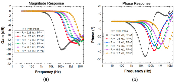
Figure 5. Bode plot of the RC low pass filter (a) magnitude response. (b) phase response.
Download figure:
Standard image High-resolution imageEach of the magnitude plots in figure 5(a) exhibits the characteristics of a low pass filter. Each of the magnitude plots showed an exponential roll-off of ∼12 dB/decade. The plot for the device with the 228 kΩ resistor (after 1 print pass), which had the lowest corner frequency at ∼7 kHz, shows a modest increase in the magnitude for frequencies beyond 100 kHz, which ultimately plateaus at 1 MHz. Such behavior is possibly due to a parasitic inductance associated with the interdigitated electrode gaps, an effect which has been observed in graphene-based RC filters [23]. Thus, the RC filter exhibits weak RLC filter-like characteristics with a resonance frequency at ∼202 kHz when R = 228 kΩ. The magnitude curve shows a trough at ∼202 kHz, corresponding to a 0° phase in the phase response.
Each of the phase plots in figure 5(b) exhibits characteristics expected of low pass filters, showing an increasingly negative phase angle when the frequency begins to exceed the corner frequency. For the RC filter incorporating the 228 kΩ resistor ( = 7 kHz), the phase angle drops to a minimum of nearly −46° at ∼29 kHz. This indicates, in the time domain, that the output voltage lags the input voltage by 46° at ∼29 kHz. At
  = 7 kHz, the phase angle is nearly −26°, which is slightly over half the phase angle at ∼29 kHz. This is consistent with the stop band characteristics of a low pass filter. Beyond 29 kHz, the phase angle begins to rise due to the parasitic inductance, until it reaches 0° at ∼202 kHz, which is the resonance frequency associated with the RLC characteristics over high frequency ranges.
The corner frequency ( ) of a low-pass filter can be calculated using:
where R is the resistance and C is the capacitance of the device [22, 23, 26]. The corner frequency of each RC filter was experimentally determined from the Bode plot by assessing the frequency at which the magnitude drops by 3 dB. In this study, a total of five sets of RC filters were fabricated with each set consisting of six RC filter devices that share a common capacitor but incorporate distinctly different resistors realized by the number of print passes used to fabricate them (1–6).
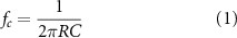
Figure 6 presents the relationship between corner frequency and resistance for the set of RC filters associated with the Bode plots in figure 5. Figure 6(a) presents a plot of the measured corner frequency versus resistance for these six RC filters. The corner frequency is observed to decrease linearly from ∼2 MHz to ∼7 kHz as the resistance is increased from ∼1.7 kΩ to ∼228 kΩ by successive print passes over the resistor. In order to relate these data to equation (1), figure 6(b) presents a plot of the corner frequency versus the reciprocal of resistance. A linear fit of these data have an R2 value of 0.9957, which indicates that equation (1) accurately describes the behavior of these filters.
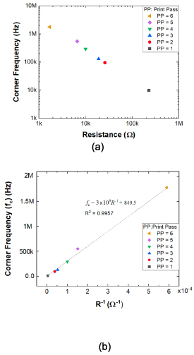
Figure 6. The relationship between corner frequency and resistance for the set of RC filters associated with the Bode plots in figure 5: (a) corner frequency versus resistance and (b) corner frequency versus inverse resistance.
Download figure:
Standard image High-resolution imageFigure 7 summarizes the relationship between the average corner frequency and average resistance for the five sets of RC filters developed in this study. Figure 7 is essentially a representation of the repeatability of the fabrication process described in this work. As with the data in figure 6(a) for a single set of RC filters, the data aggregated from the five sets also exhibit a linear relationship between corner frequency and the resistance of the resistor. According to equation (1), the corner frequency is inversely proportional to resistance. In a log–log plot, the corner frequency with respect to resistance would be linear with a slope of −1. For the data presented in figure 7, the slope of a line fitted to the average corner frequency versus average resistance was −0.952, which is within 5% of the theoretical value, indicating that equation (1) accurately describes the behavior of all filters included in this study. We believe the uncertainties in this plot are associated with run-to-run variations in RC filter geometry as well as the Zn microparticle density across the five sets of RC filters, which in turn are associated with the screen printing process and likely to be largest for the lowest resistance values.
Figure 7. Average corner frequency versus average resistance for the Zn-based RC filter devices.
Download figure:
Standard image High-resolution imageFigure 8 summarizes the relationships between the average corner frequency and the number of print passes used to fabricate the resistors for the five set of RC filters developed in this work. The average corner frequency is observed to increase significantly from ∼7 kHz to ∼1 MHz as the number of print passes increases from 1 to 6. In contrast to the plots that describe the relationship between corner frequency and resistance, the behavior in this figure is presented as a semilog plot because the number of print passes are discrete values. The data presented in figure 8 shows that the corner frequency for these Zn based devices can be tuned by the number of print passes used to form the resistor. The uncertainty in the corner frequency measurements is likely to be associated with small geometric variations in the printed structures as well as the Zn microparticle density among the five RC filter sets.
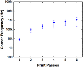
Figure 8. Average corner frequency versus number of print passes for the Zn-based RC filter devices.
Download figure:
Standard image High-resolution image3.4. Transient response
To evaluate a representative RC filter as an integrator, the transient response of select devices was characterized by applying time-varying input signals with frequencies below and above the measured corner frequency of the device and evaluating the resulting output signal. These simple tests were performed using a function generator (TTi TG35 Function Generator) and an oscilloscope (Keysight InfiniiVision MSOX3024T Mixed Signal Oscilloscope). The input excitation signal consisted of a square wave, whereas the output waveform was the measured voltage across the capacitor. Square wave inputs represent the scenario of repeated on and off direct current inputs at a fixed frequency, and therefore enable the time constant of the RC filter circuit to be determined. Figure 9(a) presents the transient response for an RC filter with a corner frequency of ∼130 kHz and a square wave input voltage (Vamplitude = 1.375 V) at a frequency of 20 kHz. As can clearly be seen, when the frequency of the excitation signal is less than the measured corner frequency (f <  ), the output signal is essentially a square wave in synchronization with the input. The time constant for this RC filter can be experimentally determined by estimating the time at which the signal reaches 63% of its final value; which for this device was ∼2 μs. The calculated capacitance from such a time constant value is ∼100 pF. Because the pulse duration of the input square wave signal was larger than five time constants of the filter device (25 μs > 5(2 μs) = 10 μs), the capacitor was fully charged during this 'on' time cycle and the output signal exhibits the square-wave like profile shown in figure 9(a). The peak of the output voltage (Vout peak = 1.14 V) is observed to be slightly lower than that of the input voltage (Vin peak = 1.22 V). In other words, the gain was ∼0.934, which, as expected, is close to unity. This small deviation (∼7%) can possibly be attributed to sampling resolution limitations of the oscilloscope. Another possible reason might be the contribution of high frequency harmonics on the RC filter device.
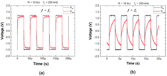
Figure 9. Transient response of the low pass RC filter. (a) Input frequency less than  = 200 kHz. (b) Input frequency greater than
  = 200 kHz.
Download figure:
Standard image High-resolution imageFigure 9(b) shows the output response for the same device when the frequency of the excitation signal was higher than the corner frequency (f >  ). For this particular measurement, the input frequency was 220 kHz. Because the pulse width of the input square wave (both charging and discharging cycle) was smaller in this case (2.5 μs < 5(2 μs) = 10 μs), the capacitor was only partially charged during a single cycle, resulting in a triangular waveform at the output. The profile of the measured output in this case is characteristic of an RC integrator and is consistent with a typical first-order RC low pass filter.
4. Material analysis
4.1. SEM analysis
Figure 10 presents low, medium and high magnification plan-view SEM images of as-printed Zn structures as well as structures subjected to 4 print passes and 8 print passes at a drop spacing of 35 µm. As expected, the low and medium magnification SEM images in figure 10(a) show that the as-printed structures are characterized by a uniform distribution of Zn microparticles in the 1–5 μm diameter range that appear to be densely packed. The high magnification image shows that these microparticles are not concatenated. The low and medium magnification images in figure 10(b) taken from the sample treated with 4 print passes also show a microstructure similar to the as-printed sample. However, the high magnification image from this sample clearly shows evidence of cold welding between two neighboring Zn microparticles. The low magnification image in figure 10(c) taken from the sample treated with 8 print passes shows a surface that appears to be more dense and less smooth than those from the other two samples. The medium magnification image from this sample shows evidence of cold welding between adjacent microparticles; evidence not seen in the medium magnification images from the other samples. The high magnification image from this sample shows that the density of cold-welded microparticles is the highest of the three samples. In fact, a network of connected structures composed of microparticles welded to multiple adjacent microparticles can be seen in the image.
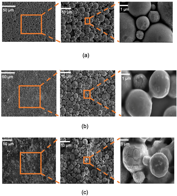
Figure 10. Plan-view low, medium and high magnification SEM images of screen-printed Zn structures: (a) as printed, (b) after 4 print passes, and (c) after 8 print passes.
Download figure:
Standard image High-resolution imageTo observe the effects of acetic acid diffusion into the screen-printed Zn structures, cross-sectional SEM imaging was also performed. Zn structures were printed on the unpolished side of a Si wafer and subjected to acetic acid exposure by RIJ for a prescribed number of print passes. The Si substrate was then cleaved to obtain mechanically sectioned samples for imaging purposes. Figure 11 presents cross-sectional SEM images from an as-printed sample as well as a sample after 8 print passes. Consistent with the plan-view images in figure 10(a), the SEM image in figure 11(a) taken from the as-printed sample shows Zn microparticles that are uniformly distributed throughout the thickness of the structure. There is no evidence of cold welding. The high image contrast between the Zn microparticles and the conducting Si substrate may be due to low intensity charging associated with the high electrical resistance of the Zn structure resulting from the native oxide that encapsulates the untreated particles. The SEM image from the sample treated with 8 print passes (figure 11(b)) indicates that the structure consists of a dense near surface region that sits atop a microparticle base. Image contrasts suggest that the dense near surface region is more conductive than the microparticle base which would be consistent with the formation of a network of cold-welded Zn microparticles.
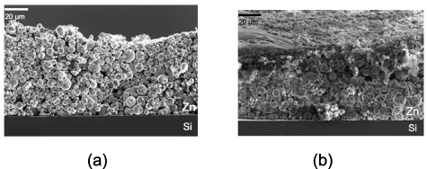
Figure 11. Cross sectional SEM images of (a) zero print passes and (b) 8 print passes.
Download figure:
Standard image High-resolution image4.2. X-ray diffraction analysis
Figure 12 presents XRD analysis of Zn structures exposed to acetic acid by inkjet printing and drop casting. The XRD spectra in figure 12(a) indicate that exposure of the screen-printed Zn structures to acetic acid does not cause a change in crystal orientation at the macroscale level regardless of the method used; therefore, the observed changes in electrical resistance with respect to the amount of acetic acid exposure cannot be ascribed to a change in crystal orientation. Figure 12(b) shows the calculated crystallite sizes for each diffraction peak in the XRD spectra presented in figure 12(a) using the Scherrer equation to calculate crystallite size (D):
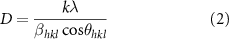
Figure 12. (a) XRD spectra of Zn samples, exposed to 4 and 8 acetic acid print passes. Spectra from an as-printed sample and a sample treated by the drop-cast method spectra are included for comparison purposes. (b) Calculated crystallite size of each spectra in (a).
Download figure:
Standard image High-resolution imagewhere k is the dimensionless shape factor (k = 0.9),  is the wavelength (=0.179 nm for Co-K alpha source),
  is the half-width of the diffraction band in radians and
  is the Bragg diffraction angle in radians.
In general, crystallite sizes range from roughly 60–80 nm depending on the crystal orientation. With respect to treatment conditions, the crystallite size associated with the (101) orientation is insensitive to acetic acid exposure. The crystallite sizes associated with the (102) and (002) peaks initially increase by ∼10 nm after 4 print passes and then decrease by roughly the same amount after 8 print passes, while the crystal size of the (001) orientation increases by ∼10 nm after 4 print passes and remains at the same size after 8 passes.
Combining the information in figure 12(b) with the SEM images in figure 10 suggest that the Zn particles are polycrystalline comprised of (002), (100), (101) and (102) grains which are largely unaffected by acetic acid exposure in terms of both orientation and grain size. Unlike thermal sintering during which the grains are significantly modified as a result of particle melting and solidifying, acetic acid exposure does not induce a modification of the crystal structure or grain size in the Zn microparticles, but rather only a chemical modification of their surfaces, resulting in a connected network of cold-welded Zn microparticles.
5. Discussion
Figure 13 presents a conceptual illustration that compares the conventional drop casting method of electrochemical sintering to the RIJ method in this work. Zn microparticles readily form electrically insulating ZnO and Zn(OH)2 oxidation layers on their surfaces when exposed to air [27]. These passivating oxides can be etched by an acetic acid/water solution through the following double displacement reactions:


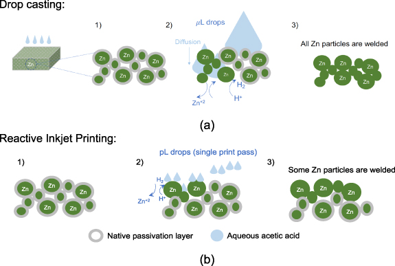
Figure 13. Concept drawing of electrochemical sintering of Zn microparticles by acetic acid using: (a) conventional drop casting and (b) the proposed reactive inkjet printing.
Download figure:
Standard image High-resolution image
The product Zn(CH3COO)2 is dissolved in water, leaving the metallic Zn exposed in the acetic acidic solution. The acidic environment enables the following Zn2+/Zn electrochemical redox reaction:

which allows dynamic dissolution and deposition of elemental Zn on the surfaces of exposed microparticles. This Zn self-exchange mechanism cold-welds adjacent microparticles into a percolated network.
In conventional drop casting, microliter drops of acetic acid are indiscriminately dispensed on the surface and diffuse into the bulk of the porous Zn microparticle structure, which dissolves the passivation layers encapsulating the Zn microparticles en masse. The combining effect of oxide etching and the subsequent chemical reactions result in the cold-welding of adjacent Zn microparticles [28] throughout the structure. This approach is effective in achieving minimum resistivity in the Zn structures but lacks the fidelity to control the resistance. In contrast, inkjet printing dispenses picolitre droplets of acetic acid in each print pass. Because the droplet volume is six orders of magnitude smaller than the droplets associated with drop casting, only a fraction of the Zn microparticles are subject to deoxidation and cold welding. Because the number of welded microparticles after a single print pass is significantly less than that associated with drop casting, the resulting electrical resistance is much higher. As illustrated in figure 1, repeated print passes using a relatively large drop spacing leads to significant reductions in electrical resistance as diffusion of acetic acid drives the deoxidation and cold-welding reactions deeper into the bulk of the structure thus expanding the network of cold–welded Zn particles with each print pass. As figure 2 implies, a small drop spacing ensures the formation of a low resistance network on the surface of the structure. Unlike conventional drop casting, the high degree of spatial control combined with pico-liter dispensing enables the side-by-side fabrication of resistors and conductors from a single printed Zn layer using the RIJ described herein. The ability to control the resistance of the resistor, not by changing the dimensions of the structure, but rather by precision dispensing of acetic acid means that a wide range of resistances can be realized in a resistor of fixed geometry. This versatility enables the room temperature fabrication of RC filters with the tunable filtering characteristics observed in figure 5 through 8 from a single printed Zn layer. This contrasts to conventional processes used to print RC filters which rely on a thermal processing step after printing to form the structure. In such cases, the corner frequency is determined primarily the geometry of the resistor.
6. Conclusions
In summary, this paper describes a process to print planar, single-layer Zn-based RC filters whose corner frequencies can be precisely tuned using a RIJ method for selective deposition of acetic acid on the printed structure. RIJ has an advantage over conventional drop casting in that both resistive and conductive patterns can be produced in the same Zn layer by leveraging the high spatial and volume control of an inkjet printer to dispense the acetic acid solution. XRD shows that acetic acid exposure does not change the crystal orientation or average size of the Zn particles. Plan-view SEM images indicate that the process dissolves the native oxide encapsulating the Zn microparticles, facilitating chemical reactions that lead to cold welding of adjacent Zn particles and the formation of a conductive network. Cross-sectional SEM images show that the depth over which cold welding occurs increases with increasing print passes. The XRD and SEM results indicate that the observed decrease in electrical resistance with increasing acetic acid exposure is solely a result of an increased prominence in cold welding which leads to an expanded network of low resistance pathways throughout the Zn structure. Use of an inkjet printer to dispense the acetic acid solution enables the resistance of the Zn structures to be precisely controlled in a manner that is not possible using other dispensing methods or thermal annealing. To demonstrate the utility of this process, Zn-based RC filters, whose corner frequency was tuned over roughly three orders of magnitude by the amount of acetic acid exposure, were fabricated from a single printed Zn layer of fixed geometry on paper substrates at room temperature. To the best of our knowledge, this is the first room temperature printing process to produce side-by-side resistors and conductors from the same printed layer and the first printing process of any type to produce RC filters with such a wide range of corner frequencies. The RIJ process demonstrated in this work utilizes biodegradable materials [29] and thus has the potential to produce printable electronics and sensors for environmental, agricultural and related applications.
Acknowledgments
This work was supported by the Advanced Platform Technology Center, Louis Stokes Cleveland VA Medical Center, OH, USA, under Grant VA250-17-P-4574.
Data availability statement
The data cannot be made publicly available upon publication because they are not available in a format that is sufficiently accessible or reusable by other researchers. The data that support the findings of this study are available upon reasonable request from the authors.