

Abstract
In this article, we report the development of a new method for the 3D printing of dielectrics. An aerosol-jet printer is used to deposit overlapping layers of photopolymer material under ultraviolet floodlight in the assembly of ramping microstructures in situ without the need for supporting structures. Printing is conducted using an in-house photodielectric ink, the development of which is presented with an emphasis on dielectric and mechanical bulk material characterization. Low dielectric loss at the X-band and structural strength are demonstrated, followed by print characterization wherein the driving mechanisms of the new method are explored, tied to print conditions, and related to specific material properties. Finally, a complex structure in the form of a 3D flower is printed to demonstrate the controlled and repeatable performance of the proposed technique.
Export citation and abstract BibTeX RIS

Original content from this work may be used under the terms of the Creative Commons Attribution 4.0 license. Any further distribution of this work must maintain attribution to the author(s) and the title of the work, journal citation and DOI.
1. Introduction
The benefits of additive manufacturing (AM) over conventional printed circuit board (PCB) technologies for electronics have recently been demonstrated in various applications [1–3], including antennas, filters, sensors, and bare semiconductor die interconnects, to name a few. In addition to reducing cost and waste, additive techniques enable the rapid prototyping of existing planar/PCB-like designs as well as the realization of flexible and/or conformal designs that were not feasible before [4, 5]. The possibilities for these designs have motivated the development of several different platforms for the deposition of conductors and dielectrics, each with its own benefits and drawbacks depending on the end use [6–8]. However, there is a constant demand for new deposition methods to augment present-day capabilities and accommodate the diverse and ever-expanding number of applications [9, 10]. This is especially true for radio frequency (RF) and microwave designs that drive emerging technologies such as 5G and the Internet of things (IoT). 5G and IoT stand poised to revolutionize the communication landscape, not only by increasing data rates and lowering latencies, but also by extending high-speed communication to a growing number of 'smart' devices. By enabling network connectivity, devices and systems that were once isolated can now work and be managed as a unit from a single screen anywhere in the world, benefiting unprecedented levels of cost and time savings to consumers and businesses alike. However, many smart devices, including wearables, health sensors, and any device integrated within a complex functional geometry (e.g. an air duct or the fuselage of a drone) are impractical due to cost or altogether impossible with PCB and other conventional techniques. Inexpensive, rapidly manufactured, flexible, and conformally printed electronics make these devices possible and are key to the success of 5G and IoT.
This paper presents a novel method for 3D printing low loss dielectric structures using photopolymer inks that are aerosol-jetted onto a substrate and simultaneously ultraviolet (UV) cured in-situ. Specifically, this is a 4D printing approach which leverages the time-varying behavior of a photopolymer under in situ UV cure, along with other parameters to be discussed, to attain a desired geometry [8, 11]. Referred to here as 'stack printing,' this phenomenon results from the incremental rastering and simultaneous curing of the photopolymer both vertically and horizontally from the bottom up. During the development of a low loss dielectric for use in traditional 2D aerosol-jet printing (AJP), print performance was characterized as a function of UV cure intensity and print speed. The ranges of these parameters were selected not only to capture print behavior under 'normal' conditions, but also to observe the effects at the extremes of the printer's commonly used range. At these points, the interplay between the amount of raster overlap, ink stream deposition rate, UV cure intensity, and print speed are significant to the novel print method to be discussed. A two-dimensional matrix of simple test structures was developed to study the relationship between the print speed and cure intensity. Upon printing the matrix, stacking was observed in the areas where the cure intensity was high and the print speed was very low, resulting in rapid and thorough curing with large linewidths and overlap ratios. Although many interesting approaches for the synthesis of 2D/3D structures have been presented, such as the graphene-based nanostructures shown in [12], the aerosol-jet printed dielectric structures reported to date have been either traditional horizontal/2D features, purely vertical or columnar stacked structures, or angular structures printed ex situ and/or requiring vertical support [13–20]. The material properties and printing conditions discussed herein enable both horizontal and vertical stacking of the overlapping lines in situ, that is, directly on the intended substrate without the need for supporting structures. Although similarly printed silver structures have also been previously reported [7, 21–25], they rely on a thermal mechanism by the diffusion of heat through the conductive structure and are not truly comparable with the method presented here.
The horizontal and vertical stacking of a direct-written dielectric presented here is a novel approach that can lead to various interesting applications requiring fine-resolution printing of complex, 3D, freestanding shapes directly onto a substrate with the potential for printing these shapes in or around existing structures; something which is not possible with other small-scale 3D printing paradigms such as stereolithography (SLA) or digital light processing (DLP). These existing structures can be 2D dielectric or conductor layers printed with AJP or other methods—such as syringe-dispense—and/or semiconductor devices integrated within an additive packaging scheme, to list a few examples. A stack printed 3D flower, further discussed below, was chosen to demonstrate both the controllability and repeatability of this print method. Comparing the in-house dielectric with NEA121, a commercially available electronics adhesive from Norland commonly repurposed for use with AJP, it was clear that properties specific to the material developed herein contribute directly to the mechanisms that enable controlled stack printing. These properties include the rate of spread/wetting after deposition, the rate of photopolymerization under UV excitation, and the resulting competition between these processes. It is evident from this work, as well as previous studies, that these material properties must be studied and optimized to develop novel 3D printed polymer architectures as reported here [26]. Therefore, presented alongside the new print method is an analysis of the dielectric formulation as well as characterization of its important properties, providing detailed insights into print performance especially as it pertains to stacking. Most significantly, a favorable surface energy profile and reduced photosensitivity allow the use of a larger regime of print settings to obtain the desired print behavior.
Beginning with the formulation of the dielectric, the molar absorptivities of a series of photoinitiators were compared to determine the strongest absorbance within the exposure range of the curing system used. Following the initiator selection, a series of photopolymer compositions representative of a diverse set of photochemical techniques were prepared. Test structures were then fabricated for electrical and mechanical characterization using both the drawdown technique and AJP. Although drawdowns allow for rapid testing of a large pool of samples, finalized test with an aerosol print ensures data consistent with the performance realized at the end use. It is important to determine the dielectric properties of materials developed for AM electronics because the complex permittivity of commercial materials is typically characterized at low frequencies (<10 MHz) [27], which can create issues when fabricating RF and microwave devices because material properties are needed at higher frequencies (>1 GHz). Moreover, the loss tangent of the materials can vary significantly at higher frequencies and can have a significant impact on device performance for RF applications. Consequently, in this study, the X-band dielectric loss is compared to demonstrate its applicability in RF designs. Dielectric characterization was performed using a transmission/reflection line (TRL) method with a WR90 (X-band) waveguide. Dynamic mechanical analysis (DMA) was then performed on the lowest loss dielectric. DMA is used to measure the dynamic modulus of the material. Compared to tensile testing, DMA provides a more compete mechanical picture with a much smaller sample size. Using DMA, the storage modulus, loss modulus, and the tan delta can be investigated over a wide temperature range. The peak and width of the tan delta can be used to decern the glass transition behavior of the material. Subsequent to DMA measurements, photo-differential scanning calorimetry (photo-DSC) was used to determine the cure kinetics, followed by contact angle measurements to provide an understanding of the substrate wetting behavior. The measured properties were then compared with those of NEA121. Finally, a detailed study of aerosol-jet printability is presented, beginning with initial print parameterization before shifting the focus to stack printing, its contributing mechanisms, and testing of its controllability and repeatability.
2. Methods
2.1. Photoinitiator selection
The photoinitiators studied in this work can be classified as either type 1 radical initiators, type 2 radical initiators, or photoacid generators. Type 1 radical initiators function through a homolytic cleavage mechanism. These initiators typically contain a characteristic aryl ketone moiety, which absorbs long wave ultraviolet (UVA) radiation. During absorption, the molecule transitions to an exited state and rearranges, resulting in the generation of a lone radical. This free radical can then enter any surrounding unsaturated bonds on surrounding monomers and initiate a free radical polymerization chain reaction. These initiators include 1 hydroxycyclohexyl phenyl ketone, 2-methyl-4ʹ-(methylthio)-2-morpholinopropiophenone, 2,2-dimethoxy-2-phenylacetophenone, and phenylbis (2,4,6-trimethylbenzoyl) phosphine oxide.
Similarly, type 2 initiators contain a sp2 hybridized region which can absorb and rearrange, typically exhibiting an anthracene-like architecture. However, unlike type 1 initiators, when type 2 initiators enter the exited state, these initiators rearrange in a way that requires the abstraction of a surrounding proton to yield a free radical. Due to this second order phenomenon, type two initiators produce radicals at a slower rate compared to type 1 initiators. Classic type 2 radical initiators include isopropylthioxanthone and benzophenone.
The third classification, photoacid generators, function through a much different mechanism compared to radical generating photoinitiators. A common photoacid generator is the onium salts. These salts contain a region of aromaticity which can absorb UV radiation and destabilize a latent counterion in the process. The counter ion then scavenges for a proton, resulting in the induction of a strong Lewis acid. The resulting Lewis acid then can act as a cation and will interact strongly with any available electron withdrawing oxirane groups, resulting in a cationic polymerization. These initiators include (4-phenylthiophenyl) diphenyl sulfonium triflate, diphenyliodonium hexafluorophosphate, diphenyliodonium p-toluene sulfonate, triarylsulfonium hexafluoroantimonate, and triarylsulfonium hexafluorophosphate.
The first step in formulating the photocurable dielectric was to choose a photoinitiator that exhibited an absorbance spectrum overlapping with the exposure spectrum of the curing equipment. A Cary 8454 UV–Vis spectrometer (Agilent Technologies) was used to compare the absorbance of the series of photoinitiators. Radical type 1 initiators were tested for use in acrylate photopolymerization, as well as cationic photoinitiators for epoxide photopolymerization. The radical initiators tested were 1-hydroxycyclophenyl ketone, 2-methyl-4ʹ-(methylthio)-2-morpholinopropiophenone, 2,2-dimethoxy-2-phenylacetophenone, and phenylbis (2,4,6-trimethylbenzoyl) phosphine oxide. For the cationic photoinitiators, the group tested (4-phenylthiophenyl) diphenyl sulfonium triflate, diphenyliodonium hexafluorophosphate, diphenyliodonium p-toluene sulfonate, triarylsulfonium hexafluoroantimonate in propylene carbonate, and triarylsulfonium hexafluorophosphate in propylene carbonate. All initiators were purchased from Millipore Sigma and diluted with gamma-butyrolactone until 1.5× absorbance was reached.
The photocurable materials were cured using a 365 nm LED array. The molar absorptivity of each radical initiator and cationic initiator are shown in figures 1 and 2, respectively. Radical initiator absorptivity data showed that only phenylbis(2,4,6-trimethylbenzoyl) phosphine oxide was absorbed at 365 nm. Therefore, phenylbis(2,4,6-trimethylbenzoyl) phosphine oxide was chosen as the preferred radical photoinitiator. For cationic initiator absorptivity, the three initiators showed similar UVA absorbance values. Triarylsulfonium hexafluoroantimonate was not used because it contains the toxic heavy metal antimony. Diphenyliodonium hexafluorophosphate was eliminated owing to its high cost. Thus, triarylsulfonium hexafluorophosphate was chosen as the preferred initiator for the epoxide initiation.

Figure 1. Radical initiator molar absorptivity between 300 nm and 400 nm.
Download figure:
Standard image High-resolution image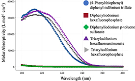
Figure 2. Cationic initiator molar absorptivity between 300 nm and 400 nm.
Download figure:
Standard image High-resolution image2.2. Monomer selection
Four photocurable polymer compositions were tested: two employing a radical-acrylate cure mechanism, and two employing an epoxide-cation cure mechanism. Radical acrylate chemistry is more commonly used in industrial photocurable coatings because of its low cost and versatility. Radical acrylate polymerizations, however, are characterized by resonance-stabilized radical propagation, which yields a rapid and uncontrollable polymerization reaction prone to oxygen inhibition [28–31]. On the other hand, epoxide cationic polymerization progresses through inductively stabilized cation propagation, a slower, more controllable reaction with no sensitivity to oxygen [32–39].
The two acrylate resins used in this study, CN131 and CN132, were purchased from Sartomer. CN131 is a derivative of bisphenol-A acrylate and CN123 is a urethane diacrylate compound. The third and fourth compositions used the epoxide monomers 3,4-epoxycyclohexylmethyl 3,4-epoxycyclohexanecarboxylate (EEC) and bisphenol-A-diglycidyl ether (BADGE), respectively. The EEC resin was purchased from Millipore Sigma, and the BADGE resin was purchased as a mix of eight-parts BAGDE and one-part trimethylolpropane triacrylate from Hexion under the trade name Epon 8111. All four resins were chosen because of their low viscosities and adhesion to plastic and metallic substrates. All resins were used as received without further purification.
Each composition was batched as 3 g samples in 20 ml glass jars covered in aluminum, sealed in nitrogen, and stirred using Teflon bars at 280 rpms for 24 h. All four compositions used 4% of their respective initiators, as described in table 1.
Table 1. Summary of the polymer composition candidate pool.
| Material ID | Ingredient used | Ingredient type | Initiator used |
|---|---|---|---|
| 1 | CN131 | Bisphenol-A acrylate oligomer | Type 1 radical initiator |
| 2 | CN132 | Urethane acrylate oligomer | Type 1 radical initiator |
| 3 | 3,4-epoxycyclohexylmethyl 3,4-epoxycyclohexanecarboxylate (EEC) | Cyclic aliphatic epoxy monomer | Photoacid generator in solution |
| 4 | Epon 8111 | BADGE epoxy oligomer/acrylate monomer blend | Photoacid generator in solution |
2.3. Dielectric test
Many techniques are available for the measurement of electric permittivity and loss tangent, including TRL, open-ended coaxial probe, and resonant cavity methods [40–42]. For its combination of accuracy and practical use when taking broadband measurements of solid materials, the TRL method was selected and configured using a Keysight X11644 WR90 waveguide calibration kit, Keysight materials measurement software suite, and FieldFox N9918A vector network analyzer [41, 43]. Broadband measurements are helpful for the characterization of unknown materials with potentially dispersive (i.e. frequency-dependent) behavior.
Using the TRL method, two-port S-parameter measurements are taken, and then the dielectric constant and loss tangent are extracted. The selection of the extraction method is also a consequence as this dictates the required material under test (MUT) sample thickness [44–47]. The Keysight software suite enabled the selection of the most accurate method with respect to the available thickness. Nicholson–Ross–Weir (NRW) extraction was chosen because of its widespread use and the sample thicknesses that can be achieved practically with the MUT's [48–51]. In the case of NRW, thicknesses less than or equal to λg/4, where λg is the guided wavelength within the MUT, are required for good accuracy. This applies across the band of interest, in this case, X-band, and requires an approximation of the permittivity of the MUT before test. Bulk MUT samples were fabricated to match the cross-sectional area of the WR90 waveguide with a thickness of 3 mm, which is sufficient for permittivity extraction using the NRW method.
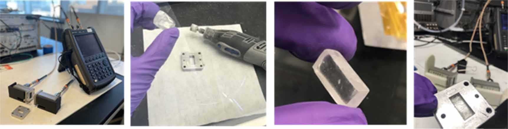
To fabricate drawdown samples for the initial tests, a doctor blade was used to administer layers of the material with 100  m thicknesses. After each layer, a PulseForge™ exposure unit was used to polymerize the material before subsequent layers were administered. The surrounding excess cured material was removed using a Dremel™ rotary tool for close fitting to the WR90 waveguide. All the samples were then heated to 150 °C for two hours to facilitate monomer conversion. This process was repeated for each material in the test pool. Images of the test setup and sample fabrication are shown in figure 3.
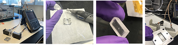
Figure 3. Dielectric test setup showing VNA and WR90 waveguide (far left), trimming of sample using a Dremel™ (middle left), finished MUT sample (middle right), and fitting into the WR90 for test (far right).
Download figure:
Standard image High-resolution imageNext, an aerosol-jet printed bulk sample of the in-house formulation was fabricated to obtain a high-quality sample for dielectric and mechanical characterization. Although the Epon composition was chosen because of its lower loss, its viscosity was among the highest tested. Therefore, to lower the viscosity and enable sufficient aerosolization, the ink in the printer was heated to 50 °C. This approach is also common practice when aerosol-jet printing NEA121 [15, 18]. Printing was performed using Optomec AJ5X Decathlon 1.0 with pneumatic atomization. This machine is equipped with 365 nm UVA LED flood lamps positioned above the print nozzle for real-time simultaneous in situ curing of photosensitive materials. To print the sample, a 300 μm print nozzle was selected to maximize material deposition (minimizing print time), and a rectangular area matching the cross-section of the WR90 was repeatedly rastered with a single pass and cured in situ at different print settings until a single layer with maximum thickness and sufficiently low surface roughness was achieved. Then, knowing that there should be little to no flow between a cured layer and subsequent layers, a special print loop code was written to programmatically raster the desired cross section with multiple layers until the thickness required for NRW extraction was reached. In this case, it was decided that a 2 mm thickness would be satisfactory and that, given a single layer thickness of 40 μm, 50 passes were necessary. A stylus profilometer from KLA Tencor was used for the thickness measurements, with step height accuracy from the nanometer range to 1200  m. Although AJP is generally insensitive to changes in the distance from the print nozzle to the print surface, or the z-height, the z-height deviation of 2 mm caused by the build-up of the structure layer-by-layer while keeping the print nozzle height constant would result in a significant alteration of the print behavior between the first and last layers. To eliminate this concern, a step increase in the print nozzle height equal to the thickness of a single layer was coded at the end of the loop, thus maintaining a constant z-height throughout the printing process.
2.4. Mechanical characterization
Following dielectric characterization, DMA was performed to understand the structural strength of the printed features. This was repeated for both the in-house formulation and NEA121, with the same drawdown samples used for the dielectric test. Specifically, the samples were measured using a tension clamp, strain of 0.02%, and frequency of 10 Hz from −30 °C to 100 °C at a ramp rate of 3 °C min−1.
As was the case with dielectric measurements, finalized bulk mechanical measurements were also performed on the aerosol-jet printed sample. Given the sizing required for each test, the same part was used for both the WR90 waveguide dielectric measurement and the DMA mechanical measurement. An image of the sample in the DMA setup is shown in figure 4.

Figure 4. DMA tension clamp with an aerosol-jet printed sample of the in-house formulation fastened into test position.
Download figure:
Standard image High-resolution image2.5. Contact angle and photo-DSC
Contact angle measurements are commonly used to analyze the surface energy relationship between an ink and substrate. Initially, contact angle measurements were used to understand the interaction between the in-house formulation and Kapton, a common conformal substrate used in printed electronics. A Theta Lite Optical Tensiometer was used to measure the contact angle of a 20  l ink sample over a 10 s period. For comparison, NEA121 was also tested using the same method.
Following the contact angle comparison, photo-DSC data were collected to analyze the cure kinetics of the in-house formulation and for comparison with NEA121. Photo-DSC measures the enthalpy released by a material when it is subjected to UV light exposure. Photo-DSC measurements were performed using a TA Instruments DSC 2500 equipped with an Omnicure S2000 high-pressure Hg lamp accessory emitting radiation between 320 and 450 nm. Approximately 10 mg of the material was used for each measurement, resulting in a sample thickness of 500 µm. Each sample was tested using aluminum pans under nitrogen and held at a 40 °C isotherm during the measurements. An exposure of 30 s at 1 watt per cm2 was used to compare the samples through differential scanning calorimetry. This dose of radiation was found to give sufficient resolution to compare the two material exotherms. A dual optical fiber guide was used so that the enthalpy on an empty reference pan could be simultaneously measured as the test sample was exposed. The enthalpy measured from the empty pan was subtracted from the sample measurements, leaving only the enthalpy released by the sample.
2.6. Optimization of print parameters
Printing was performed on an Optomec AJ5X Decathlon 1.0 with pneumatic atomization. This machine is equipped with 365 nm UVA LED flood lamps positioned above the print nozzle for real-time simultaneous in situ curing of photosensitive materials. The curing intensity is set as a percentage. Consequentially, the peak and average curing intensities at the surface of the substrate vs. machine percentage were measured using a DYMAX ACCU-CAL-50 radiometer calibrated for measurement at 320–395 nm (roughly equivalent to UVA). The results are shown in figure 5. Consistent with common practice when aerosol-jet printing other high viscosity dielectrics, the in-house dielectric was heated to 50 °C in the printer to decrease viscosity and enable better aerosolization.
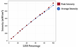
Figure 5. Plot of measured cure intensity vs. LED percentage for an Optomec AJ5X printer with UV floodlight.
Download figure:
Standard image High-resolution imageIn the first stage of testing, simple shapes and lines were printed to confirm basic aerosolization, wetting, line quality, curing, and the effects of overlap, as shown in figure 6. Subsequently, a test pattern was designed to characterize the printing performance more formally; namely, to obtain the linewidth, line/layer thickness, overspray, layer surface roughness, and adhesion while varying certain key parameters. The effects of varying the curing intensity and printer speed (and varying the raster overlap percentage consequentially with changes in linewidth due to increasing/decreasing speed) while maintaining a constant ink stream via fixed aerosol-jet flow rates were of particular interest in this study. The 2D matrix selected for the test pattern is shown in figure 7. A custom print code with nested loops was written to synthesize the matrix from a single print 'element' comprised of a rastered square, a meander line, and a rastered triangle used to characterize the printing of coatings, individual lines, and sharp-angled geometries, respectively.

Figure 6. Initial in-house dielectric aerosol-jet printability testing on Kapton polyimide substrate.
Download figure:
Standard image High-resolution image
Figure 7. Aerosol-jet print UV dielectric characterization pattern.
Download figure:
Standard image High-resolution imageThe printing process was started in the lower left of the pattern at a print speed of 0.5 mm s−1 and LED cure intensity of 10% (100 mW cm−2). Then, printing progressed to the right by programmatically adjusting the cure intensity at each new element before moving up and repeating the cycle at increased print speeds, which were also programmatically adjusted. The entire 'coupon' was thus printed from a single click, allowing for the use of this pattern as a standard benchmark for quickly testing multiple UV dielectrics consecutively. The aerosol-jet flow rates, which establish the ink stream deposition rate, were set to obtain 50 μm linewidths at 10 mm s−1 print speed and held constant throughout the print. Specifically, at a fixed print speed, the width and thickness of an aerosol-jet printed line are modulated via adjustment of the so-called atomizer and sheath flowrates. The atomizer rate is an inflow which propels the atomized ink droplets towards the print nozzle. A higher atomizer flowrate directly increases the deposition rate and thus leads to increased linewidth and line thickness, depending also on the sheath flowrate as well as the ink rheology (the latter of which is time-dependent for in-situ cure processes such as the UV cure studied here). The sheath flow collimates the ink stream at the print nozzle, providing the fine resolutions for which AJP is primarily known. A higher sheath flowrate increases collimation and thus leads to a thinner linewidth. Because the deposition rate is mostly held constant when increasing the sheath, a corresponding increase in line thickness is usually observed as well, again depending also on the ink properties. For comparison, the test coupon printing was repeated for both the in-house dielectric and NEA121. Again, the cure intensities and print speeds chosen for characterization were selected to capture the full range of print behaviors possible at a fixed deposition rate, the extremes of this range being of particular interest. All the sample matrices were printed on the metal side of a singly copper clad Kapton laminate. The copper on this laminate is rolled, as opposed to being electrodeposited, providing a smoother base for printing.
3. Results
3.1. Dielectric test
Pictures of the preliminary dielectric test samples are shown in figure 8. Table 2 summarizes the loss tangent and viscosity for all the compositions tested, including the commercially available electronics adhesive NEA121. Each of these materials exhibited a viscosity of less than 1200 cps, enabling pneumatic AJP. This series of reactive monomers was chosen with this viscosity range in mind. However, higher viscosity values can be achieved using oligomers with greater molecular weights; useful for targeting alternate printing methods such as syringe-dispense.
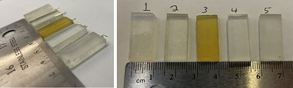
Figure 8. Drawdown photopolymer test samples fabricated for initial dielectric loss comparison.
Download figure:
Standard image High-resolution imageTable 2. Viscosity and dielectric loss of material candidates (viscosity data taken from vendor specification sheet).
| Material ID | Composition | Average loss (8.2–12.4 GHz) | Standard Dev. | Viscosity (cps) |
|---|---|---|---|---|
| 1. | CN131 | 0.0350 | 0.0017 | 210 |
| 2. | CN132 | 0.0608 | 0.0010 | 1000 |
| 3. | EEC | 0.0398 | 0.0014 | 375 |
| 4. | Epon 8111 | 0.0222 | 0.0007 | 950 |
| 5. (NEA121) | Proprietary | 0.0233 | 0.0012 | 300 |
Figure 9 shows a plot of the composition as a function of the viscosity and dielectric loss. After test, the Epon 8111 based epoxide photoacid composition emerged as the lowest loss candidate, including in comparison with NEA121. The dielectric exhibited an average loss tangent of 0.0222 ± 0.0007 between 8.12 and 12.4 GHz. In addition to offering the lowest loss, this material is also attractive from a processing standpoint. Because the Epon 8111 composition utilizes a cationic polymerization mechanism, the reaction proceeds uninhibited by oxygen. Additionally, when two propagating radicals collide with one another, the interaction yields a chemical bond between the two molecules stabilizing the radicals. When two cations interact with one another, no such bond can be made. Consequently, cationic polymerization cannot terminate through coupling. The failure of cationic polymerization to terminate through coupling reactions may aid in monomer conversion efficiency and explain the lower dielectric loss. Although the bulk dielectric performance is comparable with that of NEA121, it will be shown in later sections that the print performance is improved because of better spreading and reduced photosensitivity. Furthermore, given the paucity of research into new dielectrics for AJP, the dissemination of data for alternative materials will contribute to future advancements and spur greater interest in the area.
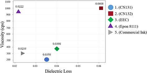
Figure 9. Plot of viscosity and dielectric loss of material candidates (viscosity data taken from vendor specification sheet).
Download figure:
Standard image High-resolution imagePictures of the aerosol-jet printed dielectric MUT sample, comprised of 50 40 μm thick layers for a total thickness of 2 mm, are shown in figure 10. A comparison of the printed sample's dielectric loss with that of the drawdown sample is shown in figure 11.
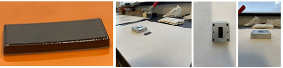
Figure 10. Aerosol-jet printed test sample on Kapton (left), sample fit into WR90 waveguide thru (right).
Download figure:
Standard image High-resolution image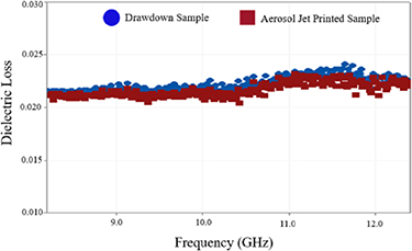
Figure 11. Dielectric loss of aerosol-jet printed sample compared with the sample fabricated via drawdown method.
Download figure:
Standard image High-resolution imageThe aerosol-jet-printed sample demonstrated a loss tangent of 0.0217 ± 0.0007 between 8.2 and 12.4 GHz, which is slightly improved compared with the initial drawdown part. This may be due to a combination of higher print quality with reduced surface roughness, enhanced curing due to prolonged UV exposure during the lengthy printing process, and/or entrapment of air bubbles between layers during printing.
3.2. Mechanical characterization
DMA measurements of the preliminary drawdown samples for the in-house formulation and NEA121 are shown in figure 12. The in-house formulation demonstrated a glass transition onset at 60 °C, peak loss tangent at 80 °C, and a 25 °C storage modulus of 6315 MPa at 25 °C. In contrast, NEA121 demonstrated a glass transition onset at 38 °C, a peak loss tangent at 60 °C, and a 25 °C storage modulus of 5593 MPa. Comparing the glass transition onset and amplitude of the loss tangent, the in-house formulation demonstrated a higher rigidity and thermal stability compared to NEA121.

Figure 12. Mechanical behavior for drawdown samples of both the in-house formulation and NEA121, with storage modulus on the left and loss tangent on the right. Measurements were completed via DMA at 10 Hz with 3 °C per minute temperature ramp.
Download figure:
Standard image High-resolution imageDMA measurements for the aerosol-jet printed sample are presented in figure 13, showing a higher glass transition temperature vs. the drawdown sample of 97.15 °C and a storage modulus of 10 179 MPa at 25 °C. Similar to the observed improvement in dielectric loss, this delta may also be due to the higher-quality sample and more thorough curing during printing.
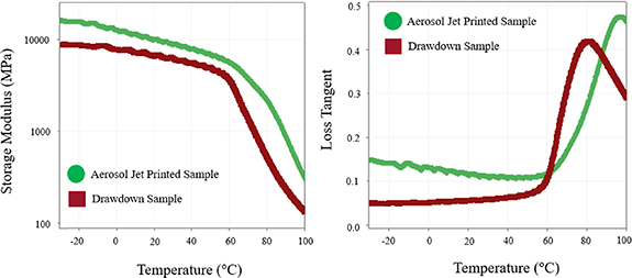
Figure 13. Mechanical behavior for an aerosol-jet printed sample of the in-house dielectric compared with that of the drawdown sample, with storage modulus on the left and mechanical loss tangent on the right. Measurements were completed via DMA at 10 Hz with 3 °C per minute temperature ramp.
Download figure:
Standard image High-resolution image3.3. Contact angle and photo-DSC
Contact angle results for both the in-house formulation and the NEA121 are shown in figures 14 and 15.
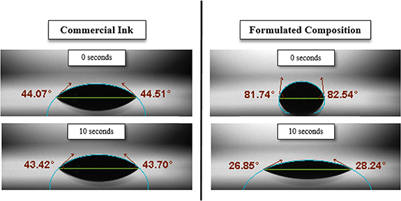
Figure 14. Contact angle profile for both the in-house formulation and NEA121 on a Kapton polyimide substrate.
Download figure:
Standard image High-resolution image
Figure 15. Mean contact angle profile for both the in-house formulation and NEA121. Data was collected at 25 °C on Kapton polyimide substrate at 0.08 s intervals.
Download figure:
Standard image High-resolution imagePhoto-DSC results are shown in figure 16.
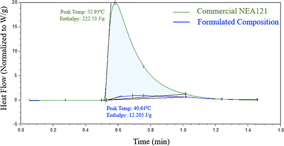
Figure 16. Photo-DSC measurements of both the in-house dielectric and NEA121, with the area under each curve representing the enthalpy released during 30 s of UV exposure.
Download figure:
Standard image High-resolution image3.4. Optimization of print parameters
The finished 4 × 3 standardized test coupon, composed of images of the individual matrix elements taken using a Keyence VHX digital microscope, is shown in figure 17.

Figure 17. Finished aerosol-jet test matrix printed on rolled copper clad Kapton substrate.
Download figure:
Standard image High-resolution imageThe bottom row of elements is the most visible because of the greater deposited volume resulting from slower print speeds. The dark 'tiger stripe' lines observed in these images are the product of uneven reflection owing to small bends in the copper laminate that occur during handling.
4. Discussion
4.1. Contact angle and photo-DSC
The contact angle data showed a major difference in the wetting behavior of the two inks. NEA121 maintained a steady contact angle on the surface of Kapton for 10 s, while the in-house formulation demonstrated a dramatic change in contact angle over the same 10 s period. The decrease in the contact angle over time exhibited by the in-house formulation may be attributed to the interaction between the aromatic and hydroxyl groups of the bisphenol-A molecule as the material contacts the polyimide Kapton substrate. This dynamic profile augments the role of the cure intensity when manipulating the print behavior. The initially high contact angle provides tight, precise, high aspect-ratio lines at higher intensities, where the ink is not allowed time to flow on the substrate before fully setting. Conversely, at lower intensities, there is more time for the ink to flow, and the decrease in the contact angle over that time results in a flatter distribution of the printed line. For rastered prints, as demonstrated below, this provides smoother surface roughness. Reduced photosensitivity—another advantage of the in-house dielectric—emphasizes this effect, providing greater control via cure intensity. In combination with print speed, this is of particular importance to the occurrence of stacking, both in terms of greater control and in the printing of flatter lines, which tend to stack more easily owing to improved structural integrity.
During photo-DSC measurement, the in-house formulation released 12.2 J of enthalpy per gram during the 30 s period of exposure, while NEA121 released 222.53 J per gram. In addition, the in-house formulation reached a peak temperature at a slower rate than NEA121 did. These major differences in kinetics validate the curing behavior observed during in situ curing. Through a delayed cure mechanism, the in-house formulation provides a more modular approach and greater control over the cure rate throughout the printing process. This allows the dielectric to settle after contact with the substrate, thereby enabling smoother and thinner pattern printing. As will be demonstrated, NEA121 was found to cure rapidly and uncontrollably, resulting in greater surface roughness owing to the immediate curing of the ink as it meets the substrate. Interpreting these results in light of the thermofluidic analysis performed in [26], relative to NEA121, the in-house formulation showed a decrease in the droplet spreading timescale,  , and an increase in the photopolymerization timescale,
  , denoting the time delays required for a single droplet to fully spread and fully cure, respectively. Although the deposition timescale,
  is much smaller than both of these (i.e. many droplets are deposited before the first can either fully spread or fully cure, allowing agglomeration into a smooth line), comparison with Case 1 of the analysis in [26] is still instructive. In this case,
  , meaning that spreading occurs completely before photopolymerization starts. In the case of our in-house formulation, the droplet spread was not completely decoupled from photopolymerization and the thermofluidic condition was likely closer to
  . Conversely, the print behavior of NEA121 can be approximated by Case 2 from [26]:
  . In this case, although the droplets can agglomerate into a single smooth line, the spreading is significantly affected by photopolymerization, and a 2D raster cannot be printed smoothly in a single pass. It is by controlling this 'competition between spreading and curing' [26] that our in-house formulation delivers greater user control. With an increase in the photopolymerization timescale (lower photosensitivity) and a decrease in the spreading timescale (dynamic contact angle), the process cure intensity became more important and could be adjusted with real, quantifiable control for tailoring prints to requirements.
4.2. 3D printing of photocurable dielectric ink
Analysis of the print data reveals important information relating the cure intensity and print speed of the printed dielectric to the surface roughness of the printed dielectric when applying a uniform coat to a substrate. When prioritizing low surface roughness, it is possible to select a combination of cure intensity and print speed that allows for 'partial' curing of the individual lines mid-print. These lines are subjected to sufficient radiation to cure in place and do not pool excessively under the aerosol-jet sheath (which is always on and can push and deform the deposition). However, it is important to ensure that the lines do not cure too rapidly and prohibit the overlapping lines from flowing into one another before fully setting. As demonstrated by the prints shown in figure 18, this resulted in a smooth but well-adhered layer of the cured dielectric. This was confirmed by a comparison of the surface roughness data measured by a stylus profilometer, as shown in figure 19. Comparing the samples printed at higher intensities (left) to those printed at moderate (middle) and lower (right) intensities, the peak-to-peak height of the 'grain' caused by the periodic rastered nature of the print is greatly reduced with the in-house dielectric. As previously mentioned, this is a direct benefit of material design in the careful tuning of the interplay between spreading and photopolymerization, as discussed in [26]. Conversely, samples printed with NEA121 exhibit significant graininess even at lower cure intensities, often necessitating additional passes for surface smoothing [15, 18]. Achieving smooth, planarized layers in a single pass allows for quick processing and maintains the thinner deposition layers for which aerosol-jet is useful and is desired in many RF and microwave applications.
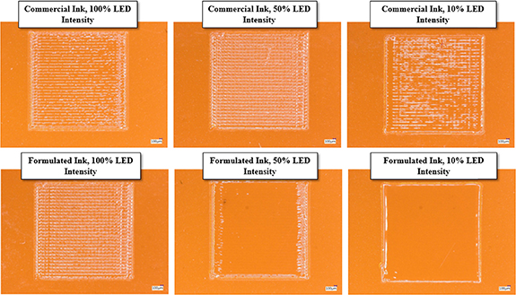
Figure 18. Aerosol-jet printed rasters showing improvement in surface roughness at lower UV exposures for the in-house dielectric vs. NEA121.
Download figure:
Standard image High-resolution image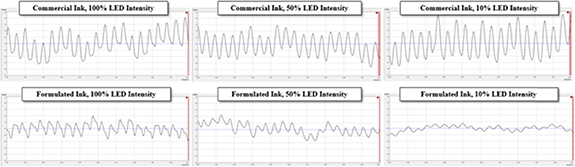
Figure 19. Surface roughness measurements for the samples shown in figure 18. Y axis values range from −6 µm to 6 µm.
Download figure:
Standard image High-resolution imageMoving into the focus of this work, the print behavior observed in the lower-middle and lower-right portions of the test pattern in figure 17 demonstrates the significance of these controlling factors in achieving not only a desired 2D print but also novel 3D structures. Specifically, sufficient overlap and appropriate curing between rastered lines (the latter being a product of both print speed and UV cure intensity) result in horizontal and vertical stacking of the overlapping lines. Pictures of the test coupon samples exhibiting this behavior are shown in figure 20.
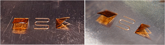
Figure 20. Test pattern samples exhibiting both horizontal and vertical stacking.
Download figure:
Standard image High-resolution imageThe differences between these samples indicate that the ratio of vertical to horizontal travel (i.e. the arctan of the angle of the structure to the horizontal) varies with UV cure intensity, thus suggesting the controllability of this phenomenon via process parameterization. Consequently, further exploration of the mechanisms that contribute to stacking and their influence on the characteristics of a given print was conducted. In order of significance, the main contributing factors were determined to be raster overlap, ink stream deposition rate, UV cure intensity, and print speed. The graphic shown in figure 21 illustrates the contributing factors and their relationships.

Figure 21. Illustration outlining important print parameters contributing to stacking along with their relationships.
Download figure:
Standard image High-resolution imageOverlap is the most significant factor, owing in part to its direct effect on the print angle as illustrated in figure 22. In addition to determining the steepness of the structure, the overlap of the rastered lines establishes structural integrity and thus the ability to stack consecutive rasters, referred to here as 'staircasing.' The deposition rate has an influence here as well, given that sufficient material must be deposited in order for more of the deposited line to cure clear of the substrate and not wet down the side of the adjacent line (as is the case with purely horizontal/2D rasters). As discussed in the section 2, together with the print speed, the deposition rate (set by the aerosol-jet flow rates) also determines the linewidth and line thickness, while overlap is usually set as a percentage of the linewidth in the print path. The UV cure intensity and print speed work together to set the amount of UV energy a printed line receives until the adjacent line makes contact. There exists some optimal amount of exposure that cures the first line in place sufficiently to provide structural support and minimize drooping while also leaving the line viscid enough that the second line can 'grab' and bond as another step in the staircase. Because print speed also helps to set the linewidth, the best practice is to establish the linewidth and line thickness via deposition rate/flowrate adjustments at a print speed that enables quicker and more efficient processing, and then adjust the UV cure intensity for optimal stacking at the chosen print speed.

Figure 22. Illustration of stack print angle and its dependence on raster overlap.
Download figure:
Standard image High-resolution imageIn total, similar to the cases studied in [26], this is a very complex thermofluidic and rheological process that is heavily dependent on material properties, including the discussed spreading and photopolymerization timescales, how the spreading timescale changes when the ink is wetted to different substrates and then to itself, and the amount of influence or coupling between the photopolymerization and spreading timescales due to increasing viscosity. By controlling the timescale coupling, the in-house dielectric enables this novel architecture within the capabilities of our specific machine (e.g. UV cure intensity and floodlight illumination). However, this method may also be possible with other materials under different conditions. Therefore, the intent of this initial work was not to present a rigorous process for printing to specific design requirements as demonstrated in [15, 52]; rather, it was meant as a preliminary exploration of the phenomenon, its influencing material and print parameters, and its control and repeatability. Future work will require more in-depth characterization and slicing algorithms for build-to-print processing, as observed in mature technologies such as fused deposition modelling (FDM) and SLA.
To confirm the controllability suggested by the matrix trials and to demonstrate the repeatability and consistency of stacking as a printing method, another test pattern was designed in the shape of a flower with three concentric rings of pedals, as shown in figure 23.

Figure 23. Flower-shaped pattern for demonstration of stack printing controllability and repeatability.
Download figure:
Standard image High-resolution imageThis structure clearly demonstrates the importance of overlap. Each ring was stack printed using different overlap percentages. To avoid interference between separate rings during and after printing, the rings were printed from outermost to innermost. At each subsequent ring, the overlap percentage was increased to gradually affect steeper slanted petals towards the center of the flower. All other printing parameters were kept constant throughout. A still-capture of a video taken during printing of the innermost ring is shown in figure 24.

Figure 24. Still-capture of flower stack printing, showing in-progress layer (adjacent to cursor) and surrounding finished petals.
Download figure:
Standard image High-resolution imageThe finished print is shown in figure 25. It is important to note the consistency in the size, angle, and print quality with which the petals are repeated. It is evident that, like FDM printing, momentary lapses in print quality propagate throughout a stack printed structure even after the lapse has been cleared. In this case, a transient deviation in the aerosol-jet atomizer flowrate from its setpoint forced a delta in the print linewidth, which, although small, was sufficient to violate the overlap percentage required to maintain a consistent angle to the horizontal.

Figure 25. Finished stack printed flower.
Download figure:
Standard image High-resolution imageThis resulted in a 'wrinkle' which is pronounced throughout the single petal circled in red. Because they are not structurally connected, the other petals are independently printed and therefore unaffected. The printing parameters are listed in table 3. It is important to note again that the flowrates are only significant insofar as they are used to establish a precise ink stream deposition rate, which often varies significantly for a fixed set of flowrates. In this case, because the flower is meant to demonstrate the effect of overlap on the print angle and not the overall print geometry/volume, only measurement of the linewidth (not shown) is required to establish the overlap percentage and thus the angle/steepness of the flower petals; flowrates are shown only for completeness.
Table 3. AJ5X print parameters for the stack printed flower.
| Temperatures | Flowrates (SCCM) | UV cure intensity | Overlap | Print speed | ||
|---|---|---|---|---|---|---|
| PA Heat | 50 °C | Sheath | 60 | 500 mW cm−2 | 80%, 85%, 95% (Outer, middle, inner rings, respectively) | 0.5 mm s−1 |
| Bubbler Heat | 25 °C | Atomizer | 1025 | |||
| PA Stir | 0.1 V, then 0 V | VI Exhaust | 0.461PSI | |||
| Platen Heat | 25 C | VI Sheath | 1025 | |||
| Chiller Temp | 20 °C | Divert | 80 | |||
| Boost | 80 | |||||
To test the reliability and robustness of this method, another sample was printed eight months after the first print using the same in-house dielectric, print parameters, and print file. The second sample, shown in figure 26, was printed successfully with no defects and with minimal adjustment to the aerosol-jet flow rates, as shown in table 4. Regarding these differences, as previously mentioned, flow rate changes are often necessary to maintain a constant deposition rate even when printing commercial inks over multiple sessions; therefore, the deltas shown are not considered significant.

Figure 26. Second flower, stack printed eight months after the first under similar conditions to show long-term repeatability.
Download figure:
Standard image High-resolution image
Table 4. Print parameters for the second stack printed flower.
| Temperatures | Flowrates (SCCM) | UV cure intensity | Overlap | Print speed | ||
|---|---|---|---|---|---|---|
| PA Heat | 50 °C | Sheath | 65 | 500 mW cm−2 | 80%, 85%, 95% (Outer, middle, inner rings, respectively) | 0.5 mm s−1 |
| Bubbler Heat | 25 °C | Atomizer | 900 | |||
| PA Stir | 0.1 V, then 0 V | VI Exhaust | 0.520PSI | |||
| Platen Heat | 25 C | VI Sheath | 900 | |||
| Chiller Temp | 20 °C | Divert | 70 | |||
| Boost | 70 | |||||
The slight 'drooping' of the petals visible in the lower images of figure 26 can be attributed to the triangular structure. As the print gets closer to the top, the raster width becomes thinner and it takes less time for the printer to move from one line to the next. Consequently, the curing per raster was reduced, and the petals began to bend under their own weight. In future work, this could be mitigated by increasing the cure intensity in a gradient towards the top of the print to compensate for the decreasing amount of time between rastered lines.
Given the ramping/angular structuring intrinsic to this method, its potential utility may be most apparent in the additive fabrication of fillets between different leveled surfaces (DLS's) such as PCB-chip interfaces [15]. In addition, although the flower geometry was chosen to demonstrate the feasibility of the novel printing method, its success suggests the possibility of synthesizing electrical and/or mechanical metamaterials. However, such an implementation would require more sophisticated electromagnetic and mechanical measurements than the simple bulk material characterization reported in this work.
5. Conclusion
A novel method for the 3D printing of dielectric structures was demonstrated using aerosol-jetted photopolymers. This is a 4D print technique which affects a time-dependent print behavior by UV curing in situ, enabling additional degrees of freedom in the printing of complex structures. By applying specific combinations of overlap, ink stream deposition rate, cure intensity, and print speed, rastered lines can be stacked both horizontally and vertically in the assembly of 3D shapes directly onto an intended substrate without the need for support. An in-house mixture of bisphenol A diglycidyl ether epoxy, polymerized through a robust cationic reaction mechanism, was used to demonstrate this method. Electrical and mechanical characterizations, analysis of print mechanics, and surface energy and photosensitivity measurements were also performed. It was concluded through this combination of material measurement and print characterization that a dynamic surface energy profile and reduced photosensitivity provide a distinct combination of the rate of spread and rate of cure required to 3D print photodielectric structures using aerosol-jet. Furthermore, it was found that precise differences in the ratio of vertical to horizontal travel could be achieved through careful control of the percentage overlap between rastered lines. To demonstrate this, a 3D flower was printed. Composed of concentric rings of flat triangular petals angled with respect to the horizontal, the petals in each ring were printed with different amounts of overlap to affect steeper petals at the inner rings. Given the consistency between petals in a single sample and between samples printed eight months apart using the same settings, it was shown that controlled stacking is repeatable both in the short term during a single print session and in the long term over multiple print sessions.
This printing method, which is enabled by the properties of the presented dielectric, can lead to many interesting possibilities. Stack printing provides advantages over other small-scale 3D manufacturing paradigms in that shapes can be printed directly onto a substrate with previously applied features, such as semiconductor devices, conductors, or other dielectrics. This is particularly advantageous in cross-platform processing. Additionally, the low dielectric loss of the ink at the X-band further extends the utility of this method to RF and microwave applications. The success of next-generation communication systems such as 5G and IoT is dependent on inexpensive printing techniques for high frequency electronics. The method demonstrated here is one such candidate for the assembly of flexible and conformal wearables, health sensors, and other network connected systems that are costly or impractical to fabricate via PCB and other conventional techniques.
Acknowledgments
This work was supported by Raytheon Technologies through their involvement in the Raytheon—UMass Lowell Research Institute (RURI) and is also embodied in two US patent applications, as referenced below.
RAY0488US/21-15166-US-NP (17/372,907) for UV formulation,
RAY0490US/21-15166-US-NP[2] (17/37,3083) for stack printing.
Data availability statement
All data that support the findings of this study are included within the article (and any supplementary files).
Conflict of interest
The authors declare that they have no known competing financial interests or personal relationships that could have influenced the work reported in this study.
Ethical compliance
None of the research reported herein involved studies on human subjects or animals.
Credit authorship contribution statement
C Areias: Conceptualization of aerosol-jet printing, methodology, writing, and data curation. Y Piro: Ink formulation conceptualization, methodology, writing, and data curation. O Ranasingha: Ink formulation, conceptualization, and methodology. A Akyurtlu: Advisor, writing, data curation: review and editing.