
Abstract
Cubic/π-SnS phase has a strong optical absorption onset and larger dielectric constant, which is favorable for solar energy conversion. Hence, these cubic SnS phase films are gaining intense interest in the research community. However, the physical properties and thus its practical application heavily depends on the synthesis condition. We present here the effects of incorporation of silver (Ag) on the physical characteristics of cubic-SnS thin films synthesized by spray pyrolysis. Ag was incorporated at different atomic concentrations of 5, 10, 15, and 20% on cubic SnS thin films. A variety of methods were used to characterize and analyze Ag-incorporated thin films. Structural and vibrational properties were analyzed using x-ray diffraction (XRD) and Raman Spectroscopy, which shows that 5 at% Ag incorporated cubic-SnS have most desirable properties. However, on higher incorporation of Ag, the deterioration of cubic SnS and formation of secondary phases (SnS2 and Sn2S3) is evident. The existence of Sn, S, and Ag ions in the necessary oxidation state has been confirmed by XPS analysis. A direct bandgap was observed in the region of 1.79 and 1.59 eV for the SnS and Ag: SnS thin films, respectively with the aid of Ultraviolet-Visible Spectroscopy (UV–vis Spectroscopy). The Photoluminescence Spectroscopy (PL) showed the near-band edge emission peak for all the samples. The needle shape morphology was observed in Scanning Electron Microscopy (SEM) images and roughness variation is estimated using optical profilometer.
Export citation and abstract BibTeX RIS

Original content from this work may be used under the terms of the Creative Commons Attribution 4.0 licence. Any further distribution of this work must maintain attribution to the author(s) and the title of the work, journal citation and DOI.
Introduction
Photovoltaic (PV) technology plays a prominent role in overcoming the energy crises in today's world. In second-generation thin-film photovoltaics, different materials are being studied to enhance the efficiency of a solar cell. The photovoltaic technologies based on GaAs, CdTe, InP, CIGS, etc exhibit a power conversion efficiency (PCE) of >20% [1]. However, the lack of raw resources, toxicity, and high cost of these materials restricts the production of these technologies on a large scale. Hence, alternative absorber materials need to be explored to overcome these issues [1, 2]. It is known that binary compounds with two elements have lower degree of complexity than that of ternary and quaternary compounds. Also, in the case of binary compounds it is easy to control the stoichiometry and thereby less chances of getting secondary phases [3]. In this scenario, SnS (Tin sulfide) is considered a promising alternative material due to its abundance and environmentally benign elements. Moreover, SnS material exhibits a desirable direct bandgap (1.2 to 1.8 eV) and the absorption coefficient is >104 cm−1 making this material apt for the absorber layer [4–6]. Although the theoretical power conversion efficiency (PCE) has a limit of up to 24%, nevertheless the experimental PCE has reached only 4.36% [7].
The SnS exhibits polymorph crystal structures of orthorhombic (stable state) and cubic (metastable state). Among that, a metastable cubic SnS shows a band gap in a range of 1.6 to 1.8 eV and an absorption coefficient >105 cm−1. Moreover, the change in the physical properties of this material as compared to its ground state structure i.e., orthorhombic makes it suitable for various applications. However, the cubic-SnS material's photovoltaic performance has been less explored [8]. Therefore, the physical properties of cubic-SnS need to be examined in detail to improve its PV performance. The well-known phases of tin sulfides include SnS, SnS2 and Sn2S3. Sn is present in +2 oxidation state in both SnS and SnS2, whereas mixed oxidation states, +2 and +3 will occur in Sn2S3. SnS exhibits two crystal structures, one being orthorhombic which is the stable state and the other is cubic, a metal stable state. SnS2 being a layered structure has hexagonal crystal structure and Sn2S2 shows orthorhombic structure [9]. The cubic-SnS thin films have been deposited utilizing various deposition techniques, such as thermal evaporation [6, 7], atomic layer deposition [10], chemical bath deposition [11], aerosol-assisted chemical vapour deposition [12], and spray pyrolysis deposition [10–15]. Among the methods, spray pyrolysis is a facile and affordable technique to deposit a thin film. Additionally, this method can deposit thin films on a large scale [16]. Therefore, in this study, the spray pyrolysis technique was employed to deposit cubic-SnS thin films.
Researchers have employed numerous approaches namely, post-deposition annealing [17–19], doping with different elements [16, 20–26], etc to enhance the physical properties of cubic-SnS. Among those, doping is one of the efficient strategies to tune the physical properties of SnS material. The optimal doping element and concentration can substantially enhance the structural, optical, morphological, and electrical properties of SnS thin films. Thus, the effect of various dopants on the properties of SnS thin film has been explored. The impact of Indium (In) doping on the chemically synthesised SnS thin film was investigated by Huang, Jian et al [27]. Their results showed higher crystallinity and a desirable bandgap of 1.56 eV was attained for films deposited using 6 at % of In. A significant enhancement in the structural and optical properties has been noticed for the In-doped SnS thin films as compared to the pristine-SnS. Akkari et al [25] studied the influence of copper dopant (5 at%, 6 at%, 8 at%, 9 at%, and 10 at%) on chemically deposited SnS thin films. The optimal copper doping concentration i.e., 6 at% shows considerable enhancement in the physical properties in comparison with other samples.
Santhosh Kumar et al [28] reported a study on the physical properties of spray pyrolyzed Ag: SnS thin films. Ag with different doping concentrations of 2–10 at% was examined. The prominent enhancement in the physical properties was noticed for the Ag: SnS as compared to the pristine SnS. Further, the films deposited using 8 at% of Ag shows better crystallinity and optimal optoelectronic properties in comparison with other dopant concentration. Ag-doped SnS thin films (SnS:Ag) and CdS/SnS solar cells with an Ag dopant concentration in the absorber varying from 0 to 6 wt% in steps of 3 wt% were made using the nebulizer-assisted spray pyrolysis method (NSP), and their properties were examined by S. Sebastian et al [29]. The device made with 3 weight percent of Ag on SnS thin films had the maximum efficiency (0.285%) because of its improved electrical characteristics, optimal bandgap, and increased absorption. Chemical synthesis of silver doped SnS absorbers (0–15 at%) with tuneable optoelectronic characteristics was carried out by Sreedevi Gedi and colleagues [30]. The deposited films showed polycrystalline characteristics, and up to 9% Ag-doping concentration enhanced the crystallinity. Because of the interstitial inclusion of Ag-atoms, the SnS films grown with a 9 at% Ag-doping concentration showed an extremely low electrical resistivity of 6 Ω-cm and a carrier concentration of 1.2 × 1016 cm−3, with an optical energy band gap of 1.26 eV.
The aforementioned studies show the significance of dopants on SnS thin film properties. Further, the Ag dopant exhibited a prominent enhancement in the physical properties of SnS thin film. However, to the best of our information, the impact of Ag doping on spray-pyrolyzed cubic SnS thin films has not been reported so far. Thus, in the present study, the role of Ag dopant on cubic-SnS thin film was explored to improve its absorber layer properties. A wide range of characterization techniques, including x-ray diffraction (XRD), Raman Spectroscopy, x-ray Photoelectron Spectroscopy (XPS), Ultraviolet-Visible Spectroscopy (UV–vis Spectroscopy), Photoluminescence Spectroscopy (PL), Optical Profilometer, Scanning Electron Microscopy (SEM), and Energy dispersive spectroscopy (EDS) were used to examine the properties of Ag incorporated films. The observations attained from this study will provide assistance to enhance PV device performance.
Experimental procedure
The synthesis of cubic SnS thin films was performed via the chemical spray pyrolysis technique. The soda-lime glass substrates were carefully cleaned using the Labolene solution. Following that, ultrasonication of the slides were carried out for 15 min each in double distilled water, acetone, and isopropyl alcohol. The details of deposition parameters are provided in table 1. A blast of dry nitrogen gas was used to dry the sample just before the deposition. The stannous chloride dihydrate (SnCl2.2H2O) and thiourea (CH4N2S) with molar concentrations of 0.05 M and 0.065 M respectively were utilized as a precursor [31]. AgNO3 solution was added to the aforementioned precursor solution, as a source of Ag dopant, at various concentrations (0, 5, 10, 15, and 20 at.%). The precursor solution is acidic in nature with a pH value of 0.7.
The structural parameters of the deposited thin films were analysed using an x-ray diffractometer (Rigaku mini flex 600) with Cu-Kα radiation with λ = 1.5406 Å. The i-Raman plus (B & W Tek Raman spectrometer) has been used to obtain the Raman spectra with the backscattering configuration at an excitation wavelength of 785 nm. X-ray Photoelectron Spectroscopy (XPS) measurements were carried out by using the Thermo Fisher K-Alpha model. The optical properties of the films were recorded using UV-Shimadzu 1800 spectrometer in the wavelength range 190–1100 nm. Zeiss Sigma field-emission scanning electron microscope was utilized for the morphological examination. MicroXAM-800 Optical profilometers from KLA corporation were used to measure sample thickness and surface roughness. All the films had an average thickness of 650 ± 50 nm. Oxford Energy dispersive spectroscopy was utilized to quantify the elemental analysis. The room temperature photoluminescence spectra (PL) have been measured employing a JASCO spectrofluorometer, FP 8500 with an excitation wavelength of 723 nm.
Results and discussion
XRD studies
Figure 1 depicts the XRD pattern of spray-pyrolyzed cubic SnS films with various Ag concentrations. Obtained patterns were compared with cubic SnS (JCPDS 77-3356), orthorhombic SnS (JCPDS 39-0354), SnS2 (JCPDS 40-1467), and Sn2S3 (JCPDS 39-0354). The XRD pattern of the undoped film closely resembles the metastable cubic SnS phase [32]. The characteristic triple peaks at 2θ angles in the 30–33° range correspond to (4 0 0), (4 1 0), and (3 0 0) planes confirmed the formation of the cubic-SnS phase [33]. Furthermore, the peak of (2 2 2) differs from the orthorhombic SnS pattern and is also associated with the cubic SnS XRD pattern. Further, we observed an improvement in the crystallinity and crystal size corresponding to the incorporation of 5 at % of Ag into cubic SnS. Thus, the formation of cubic SnS was encouraged by the additional nucleating centres from the dopant atoms, which might lead to an increase in the crystallinity of cubic SnS thin films [34]. The crystallinity and crystal size reduce drastically as the dopant atomic percentage increases to 10. The noticed reduction might be ascribed to the saturation of nucleating centres. Moreover, the difference in ionic radius of Ag (1.22 Å) and Sn (0.93 Å), leads to the increase in lattice distortion, which intensifies the strain on thin film [34]. S. Sebastian et al also reported a similar tendency in their work [29]. The addition of Ag increases the occurrence of secondary phases such as Sn2S3 and SnS2 on SnS thin films by adding a higher amount of Ag i.e., higher than 5% results in the distortion of the cubic SnS crystal structure. The visualized changes in the major XRD peaks 30–33° confirm the distortion of the cubic crystal structure. Apart from that, the XRD peak at the plane of (222) exhibits the broader peaks for films with higher Ag incorporation.
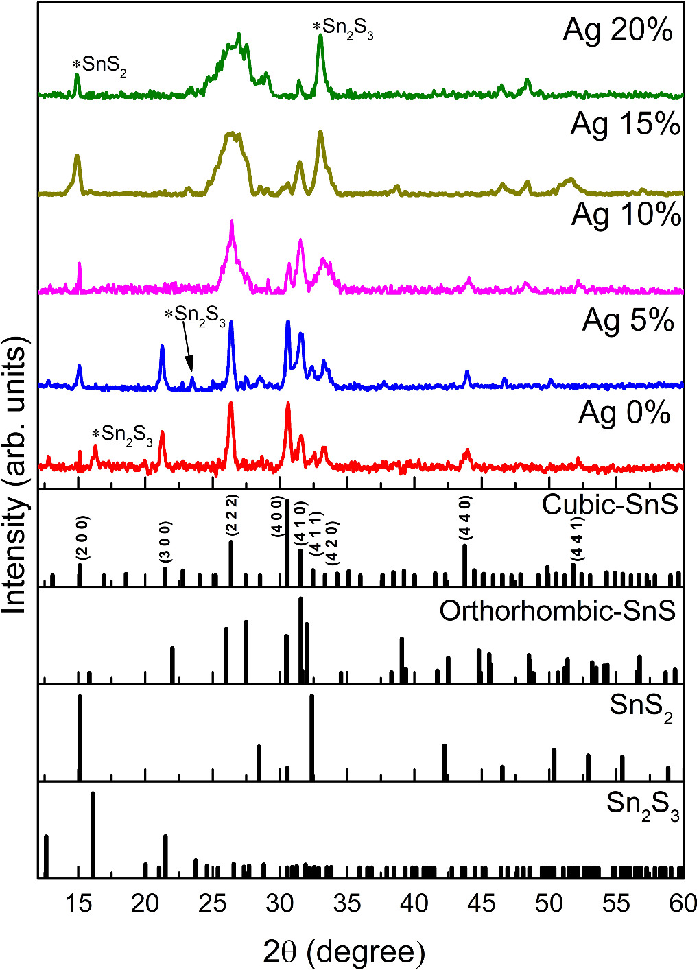
Figure 1. XRD pattern of SnS: Ag thin films at various Ag percentages.
Download figure:
Standard image High-resolution imageScherrer's relation was used to interpret the crystallite size through the XRD spectra [29],

where β is the FWHM (rad), θ is the Bragg's angle (rad), λ stands for x-ray wavelength (Å), D is crystallite size (nm). Micro-strain was determined by the equation

whereas dislocation density was computed by the relation,

Table 2 displays the fluctuation in microstructural properties of Ag-incorporated cubic SnS thin films by doping various concentrations.
Table 1. Optimized parameters of spray pyrolysis deposition.
| Parameter | Value |
|---|---|
| Substrate temperature | 325 °C |
| Flow rate | 1 ml min−1 |
| Nozzle to substrate temperature | 16 cm |
| Volume of solution | 8 ml |
| Carrier gas | Air |
| Carrier gas pressure | 1.2 bar |
| Solvent | Doubled distilled water |
| Deposition time | 10 min |
Raman spectroscopy
Raman spectroscopy measurements were carried out to determine the vibration modes of Ag-doped SnS thin films. Figure 2 displays the recorded Raman spectra of cubic SnS: Ag thin films from 100 cm−1 to 350 cm−1. Each tin sulphide phase has different vibrational modes [35]. The irreducible representation for cubic SnS, orthorhombic SnS, SnS2 and Sn2S3 phases are given respectively as [36–38],


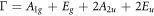

According to the spectra, the Raman modes observed at 112 cm−1, 165 cm−1, 190 cm−1, 265 cm−1, and 220 cm−1 agreed with the existing literature and are corresponds to the cubic SnS phase [39]. Besides this, all the samples showed a peak around 300 cm 1, which corresponds to the vibrational mode of Sn2S3. This result is consistent with the XRD results where all the samples (even undoped one) showed little amount of Sn2S3 phase. But as the doping concentration increases, i.e., at 15 and 20 at%, the Sn2S3 and SnS2 phases become dominant which can be observed through two major peaks 300 cm−1 and 320 cm−1 respectively [22]. This was already reflected in the XRD pattern where the diffraction peaks corresponding to the Sn2S3 and SnS2 were intense.
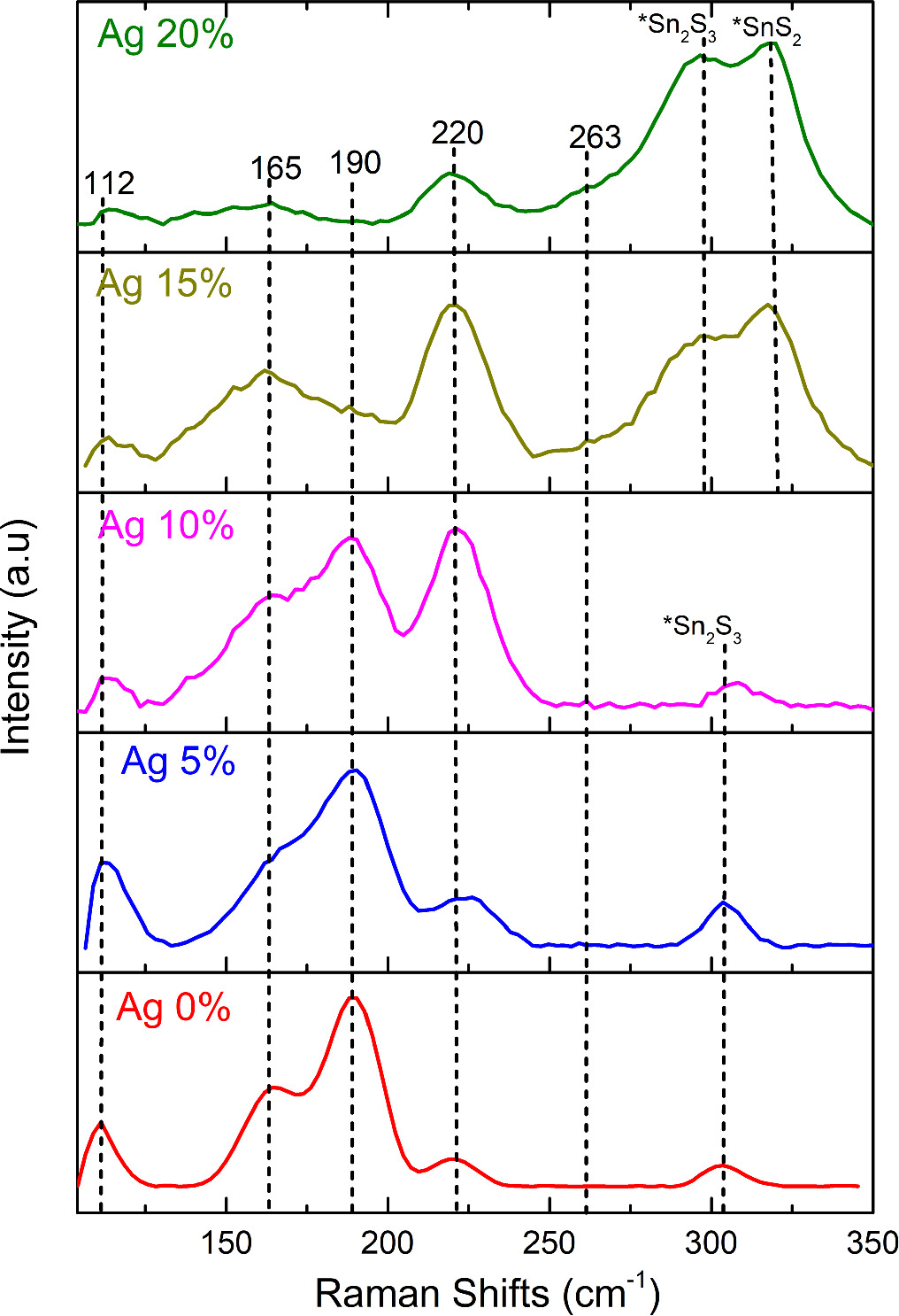
Figure 2. Raman spectra for SnS: Ag thin films.
Download figure:
Standard image High-resolution imageX-ray photoelectron spectroscopy
The XPS analysis was performed on undoped SnS and 5% of Ag-doped SnS thin film (figure 3). The XPS spectra show the presence of Sn, S, Ag, O and C and it is calibrated based on carbon 1 s peak (284.5 eV). The existence of Sn and S elements in both the film (i.e., Ag 0 at. % and Ag 5 at. %) are identified. Minor Ag peak was found at 375 eV for the Ag 5 at.% film [26], and its low intensity is ascribed to the small amount of Ag present in the film. The O and C exhibit higher intensity peaks which are presumably due to ambient contamination and the surface was not etched prior to the XPS scanning. In addition, there were no other elemental impurities were noticed in the film. The XPS spectrum of Sn in figure 3(i) shows Sn 3d at 494.9 eV corresponding to the Sn 3d3/2 energy level. In figure 3(ii) the peak at binding energy (BE) of 161.4 eV corresponds to S−2p3/2 of SnS [30, 32], which is ascribed to the S2-–Sn2+ bonding [40]. A small peak was observed by deconvoluting at 500.9 eV which may be corresponding to Sn4+, as it has a higher positive oxidation state than Sn2+, besides it promotes oxidation and over time it reacts with atmospheric oxygen, resulting in the formation of SnO2 on the surface. Figure 3(vi) shows the peak at 538 eV which belongs to the oxygen and confirms the presence of oxides on the surface [41].
Figure 3. X-ray photoelectron spectroscopy (XPS) spectra of SnS and SnS: Ag at. 5% thin films. (i) Survey Spectra, (ii) Ag 3d core spectra, (iii) C 1 s core spectra, (iv) Sn 3d core spectra, (v) S 2p core spectra, (vi) O 1 s core spectra.
Download figure:
Standard image High-resolution imageUV–vis spectroscopy
The absorption coefficient and Transmittance % versus wavelength in the range of 425–1100 nm for Ag: SnS films are depicted in figures 4(i) and (ii). The SnS thin film deposited using 5% of Ag exhibited a higher absorption coefficient and low transmittance in the visible region in comparison with other thin films. The direct energy band gap was determined using standard Tauc's relation as showen in figure 4(iii). The narrowness in the band gap was observed for the Ag-incorporated SnS thin films. The pristine SnS thin film exhibits a band gap of 1.79 eV. Overall, the narrow band gap of 1.59 eV was obtained for the Ag (5 at %) incorporated SnS thin film. When Ag incorporation is increased to 10 at.%, 15 at.%, and 20 at.% and corresponding bandgap widens to 1.65 eV, 1.66 eV, and 1.70 eV respectively [42]. This widening of the band gap can be explained based on Burstein–Moss (BM) effect. According to this effect, at the higher dopant concentrations the charge carrier concentration is very high and Fermi energy moves into the conduction band. Since the lower states of conduction bands are blocked, the excess electrons are supposed to enter the conduction band (above the fermi energy level). This leads to the increase of the band gap of a material at higher doping concentration [40, 43].
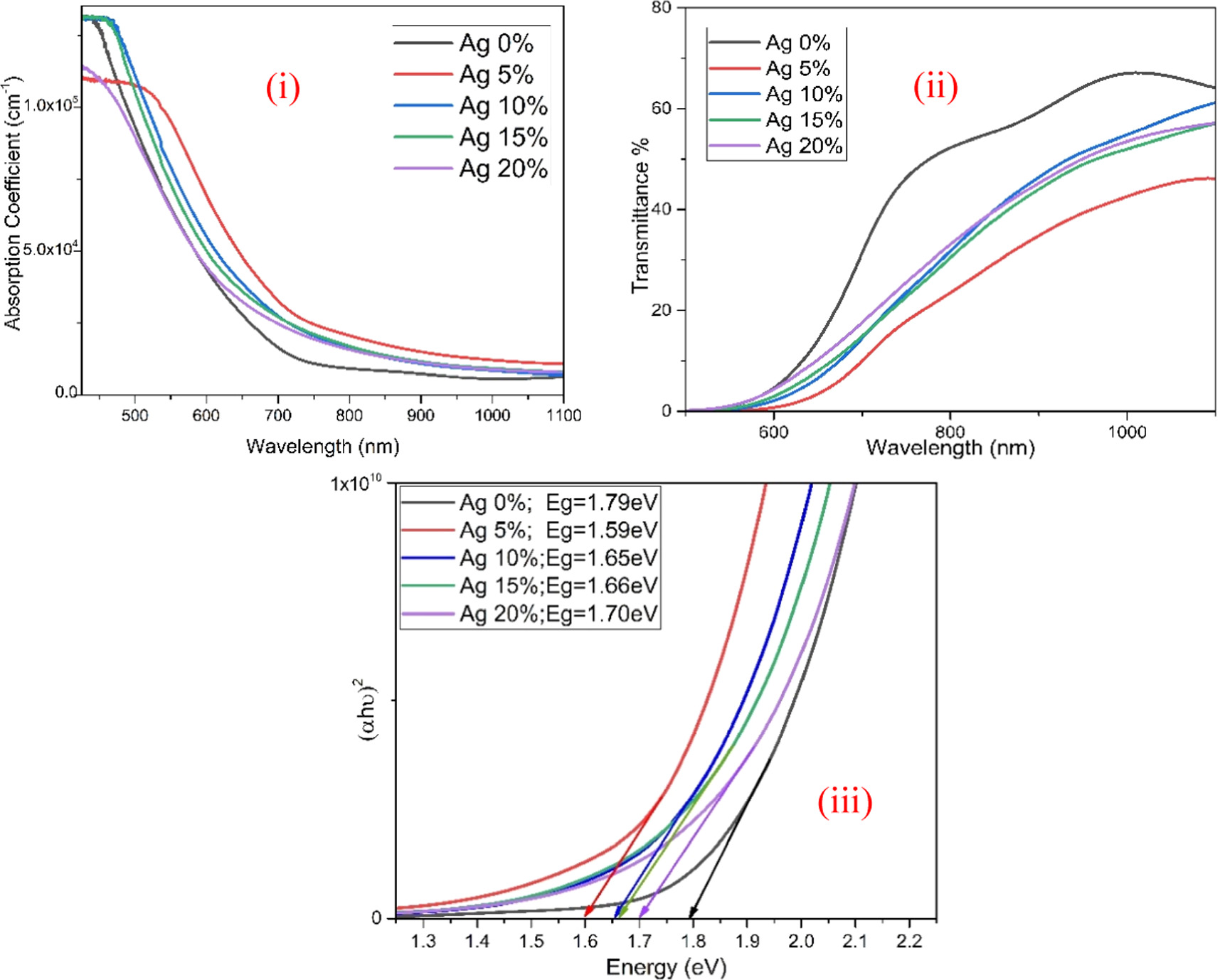
Figure 4. (i) Absorption coefficient plot, (ii) Transmittance plot, (iii) Tauc's plot for SnS: Ag thin films.
Download figure:
Standard image High-resolution imagePhotoluminescence spectroscopy
Room temperature photoluminescence (PL) spectra for the thin film SnS: Ag is shown in figure 5. The excitation wavelength 723 nm was used in this study. All the thin films displayed a strong peak around 823 nm corresponding to the near-band-edge emission (NBE) [44]. Due to the significant Sn and S vacancies at the lattice structure of undoped SnS might be responsible for its lower intensity, in comparison with SnS: Ag [45]. The incorporation of 5 at.% of Ag might lead to the reduction in Sn defects thus it exhibits a higher peak intensity. Ag has a larger atomic radius than Sn, which facilitates lattice distortion resulting in the reduction in peak intensity for 10 and 15 at.% of Ag. The noticed higher intensity at 20 at.% of Ag, indicating the formation of more stable secondary phases with fewer defects. Further variations in the emission peak strength might be related to changes in the crystallinity [18].

Figure 5. Photoluminescence spectra of SnS: Ag thin films.
Download figure:
Standard image High-resolution imageEnergy dispersive x-ray spectroscopy
The composition ratio and elemental percentage of SnS: Ag thin films are tabulated in table 3. All the films show sulfur deficiency due to its evaporation during the thin film formation. Further, the at.% of Ag in thin films was increased corresponding to its addition in the precursor solution. Concurrently, the reduction in the Sn at.% was noticed as Ag increases. The pristine SnS thin films show 63.2 at.% of Sn. The films with 20% of Ag show a significant reduction in Sn to 48.5 at.%. The Ag elemental atomic percentage of 2.0, 6.1, 9.7 and 12.5 were estimated for the 5, 10, 15 and 20% of Ag-incorporated SnS thin films. Besides that, Ag/Sn ratio increases from 0.03 to 0.25 for the Ag-incorporated SnS thin films.
Table 2. Some structural properties of cubic SnS: Ag thin films.
| Sample | Peak position (2θ) | FWHM (2θ) | Crystalline size (nm) | Dislocation density (m−2) (×1015) | Micro strain (×10−3) |
|---|---|---|---|---|---|
| Ag-0 at.% | 26.34 | 0.34 | 24.4 | 1.68 | 1.48 |
| Ag-5 at.% | 26.37 | 0.30 | 28.1 | 1.26 | 1.29 |
| Ag-10 at.% | 26.44 | 0.72 | 11.7 | 7.23 | 3.08 |
| Ag-15 at.% | 26.45 | 1.77 | 4.7 | 43.51 | 7.56 |
| Ag-20 at.% | 26.67 | 2.17 | 3.9 | 64.93 | 9.23 |
Scanning electron microscopy and optical profilometer study
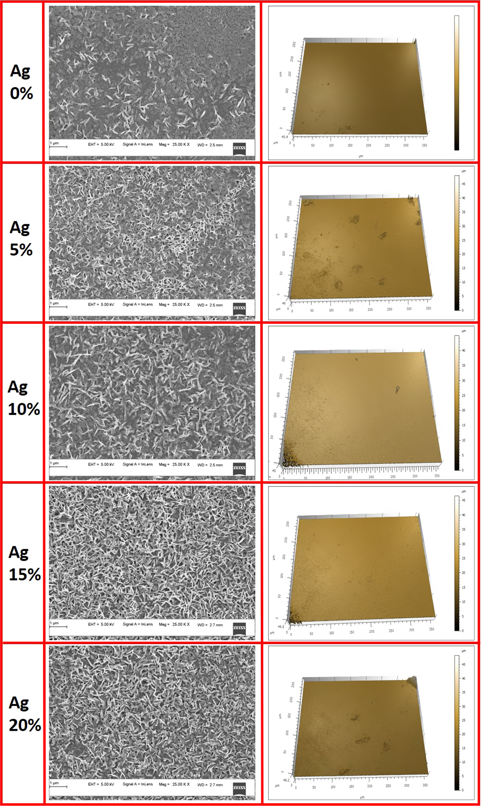
Figure 6 displays Scanning Electron Microscopy (SEM) images and Optical Profilometer 3D images of SnS: Ag films that were deposited by varying the Ag concentration. The needle-like nanostructure was noticed for pristine SnS thin films. The distribution of needle-like nanostructure significantly increases for the Ag-incorporated SnS thin films as compared to the pristine sample. As the silver concentration increased to 10% and 15%, there were some small grain-like structures in between the needles were observed. At 20% doping, we noticed the coalescence of these grains and needles. Thickness of the films were measured using the optical profilometer [Model: KLA corporation, CA, USA (MicroXAM-800). In addition to that, the surface roughness of thin films was estimated using an optical profilometer and are tabulated in table 4. The pristine SnS thin films show a roughness of 14 nm and it is considerably increased for the Ag-doped SnS thin films. The film deposited using 20% of Ag shows a higher roughness of 55 nm. The Ag-incorporated SnS thin films show the dark agglomerated patches in the profilometer which might be responsible for its increment in roughness.
Figure 6. SEM images and Optical profilometer 3D images of SnS: Ag thin films.
Download figure:
Standard image High-resolution image
Table 3. Elemental atomic percentages of SnS: Ag thin films.
| Elements (at %) | |||||
|---|---|---|---|---|---|
| Sample | Sn | S | Ag | [Sn/S] % | [Ag/Sn] % |
| Ag 0 at.% | 63.2 | 36.3 | 0 | 1.7 | 0 |
| Ag 5 at.% | 57.3 | 40.7 | 2.0 | 1.4 | 0.03 |
| Ag 10 at.% | 56.6 | 37.3 | 6.1 | 1.5 | 0.10 |
| Ag 15 at.% | 56.1 | 34.2 | 9.7 | 1.6 | 0.17 |
| Ag 20 at.% | 48.5 | 39.0 | 12.5 | 1.2 | 0.25 |
Table 4. Average surface roughness of SnS: Ag thin films.
| Sample name | Avg. surface roughness (nm) |
|---|---|
| Ag 0 at.% | 14 |
| Ag 5 at.% | 31 |
| Ag 10 at.% | 20 |
| Ag 15 at.% | 47 |
| Ag 20 at.% | 55 |
Conclusion
This article presents a study on the impact of silver incorporation on the structural, morphological, elemental, and optical properties of spray-pyrolyzed cubic SnS thin films. Using the spray pyrolysis method, thin films with varying Ag percentages were deposited and respective samples were analyzed using wide variety of advanced characterization tools. The XRD data revealed the formation of a metastable cubic-SnS crystal structure, and films deposited with 5% Ag:SnS exhibited higher crystallinity compared to other samples. Raman spectroscopy validated the formation of the cubic SnS phase, and it was observed that films coated with a greater Ag content showed an increase in the secondary phase. XPS analysis confirmed the presence of Ag on Ag:SnS thin films. A band gap of 1.5 eV was obtained for the films synthesized employing 5% of Ag:SnS, while a decrease in the bandgap was seen for the other Ag-incorporated SnS thin films. PL spectroscopy revealed significant emission at 823 nm, or near-band-edge emission (NBE). The needle-like structures were noticed on the surface micrographs, and the optical profilometer showed the lower surface roughness for all the samples. The Ag incorporation showed a significant enhancement in the physical properties of the Ag: SnS, which is beneficial to improve the performance of PV devices. The results from this study demonstrated the impact of Ag dopant on SnS thin films and provided insight to improve the PCE of SnS-based PV devices.
Acknowledgments
The authors would like to thank the Manipal Academy of Higher Education (MAHE) for providing necessary research and library facilities. The authors wish to acknowledge, Dr Sajan D George, Department of Atomic and Molecular Physics, Manipal Academy of Higher Education (MAHE) for providing Raman characterization facility.
Data availability statement
All data that support the findings of this study are included within the article (and any supplementary files).
CRediT authorship contributions
Kishore Bhat T R: Conceptualization, Investigation, Formal analysis, Writing- original draft. Pramitha A: Conceptualization, Visualisation, Investigation, Validation, Writing- review & editing. Jeganath K: Validation, Resources, Writing- review & editing. Dr Raviprakash Y: Conceptualization, Visualization, Validation, Writing- review & editing, Resources, Supervision.
Statement of conflicts of interest
The authors declare that they have no known competing financial interests or personal relationships that could have appeared to influence the work reported in this paper.