
Abstract
Herein, we report the study on RF-sputtered transition metal oxide thin films of Zinc oxide, Magnesium oxide, and Aluminum oxide as an antireflection coating on silicon-based solar cells and their influence on energy conversion. The transmission spectrum of all sputtered metal oxides was studied using a UV-visible spectrophotometer. The phase formation and microstructure analysis of these sputtered oxides were studied using glass for the destructive test along with the device. The x-ray diffraction and cross-section scanning electron microscopy of sputtered glass confirmed a single-phase structure along with nearly equal desired deposition thickness. The thicknesses of sputtered films were estimated using variable angle ellipsometry and the same was confirmed from cross-section scanning electron micrograph. The chemical composition and oxidation state of thin films deposited on glass were established from x-ray photoemission spectroscopy. The ability of a fabricated device deposited with the antireflection layer in converting photon energy to electrical energy was studied using a solar simulator under 1 sun condition. The ability to collect charge carriers of the anti-reflection coated device as a function of wavelength was also studied using quantum efficiency measurement.
Export citation and abstract BibTeX RIS

Original content from this work may be used under the terms of the Creative Commons Attribution 4.0 licence. Any further distribution of this work must maintain attribution to the author(s) and the title of the work, journal citation and DOI.
1. Introduction
In recent times, transition metal oxide (TMO) thin films have gained immense interest among researchers due to their superior optical and electrical properties [1]. TMOs offer themselves as excellent candidates for electrical and optoelectric applications due to the wide range of work function values around 3–7 eV and noticeable p- or n-type semiconductivity [2, 3]. The wide range of work functions in TMO enables them for using as an antireflection coating (ARC) on photovoltaic devices to improve photon to electron conversion (PEC) efficiency [4]. The ARCs are characterized by broad bandgap along with wide optical transmission ranging from700 to 1000 nm, and surface roughness [5]. Hence, ARC's developed in nanometer thickness can enhance the PEC efficiency of solar cells by increasing light trapping in the active region [6].
Nanostructured TMOs like ZnO, MgO, Al2O3 thin films offer exciting optical and electrical behavior when deposited in nano-level thickness [7–9]. Due to surface inhomogeneities and limited lattice periodicity, the TMOs at nanometer thickness exhibit good optical transparency, along with an appropriate refractive index [10]. Thus, they readily respond to any physical changes, which greatly affect the optical and surface conductivity of the nanostructures. The TMOs with inhomogeneous microstructure, when deposited on a photovoltaic device, creates a textured surface and thereby traps photons of light, leading to a broadband suppression in reflection. The TMO used as ARC are wavelength sensitive and reduce the reflection of incident radiation due to interference [11].
Among them, ZnO is an attractive material with superior dielectric behavior in the nanometer range and also used as transparent conducting oxide when doped with a small quantity of Al2O3 [12]. However, both ZnO and Al2O3 are also used as ARCs due to their better electrical and optical behavior including good optical transparency, appropriate refractive index and ability to form textured coating [13]. An earlier report also suggests that the TMO films deposited on Si wafer as ARC's demonstrated better device performance compared with a TiO2 single layer as ARC [14]. However, comparative studies on TMOs as ARC on silicon-based solar cells are indeed fewer. Thus, the objective of the work is set to develop transparent thin layers of ZnO, Al2O3, and MgO as an ARC layer on the top surface of the device and thereby compare their influence on PEC efficiency.
2. Experimental
2.1. Device fabrication
P-Type silicon wafer was cleaned using RCA (Radio Corporation of America) process in which silicon wafer is rinsed in H2O: HF solution for 10 min around 75 °C followed by H2O2: HCl for 10 min Later, this cleaned wafer was kept in a tube furnace for pyrogenic oxidation for the growth of the silicon oxide layer at 1100 °C to get SiO2 with a dense microstructure layer. The S1813 photoresist (PR) layer was deposited on the wafer by spin coating (made: laurel spin coater). The mask aligner (model: MJB4) was used to define the device area and imprint multiple 1 cm × 1 cm patterns on the wafer using ultraviolet (UV) rays and the PR layer. The PR from the non-patterned area was cleaned by the developer. The patterned wafer was immersed in buffer oxide etch (BOE) solution and subsequently in water: HF solution to make it more hydrophobic. The n-type layer was deposited by diffusion of PoCl3 in bubbler furnace to get the resistance of 30 Ω/cm2. The 1μm thick front aluminum layer was deposited using e-beam evaporation technique. Further, the contact pattern was printed using a photoresist and mask aligner tool by UV rays. The photoresist layer was again removed by using the developer and baked for 110 °C for a minute. In order to remove the exposed Aluminum, the wafer was dipped in PAN(H3PO4:HNO3: H2O) solution and thereafter cleaned with acetone, isopropyl alcohol (IPA) and deionized (DI) water consequently. Post front coating, a thin layer PR (S1813) layer was coated using the spin processor and baked at 110 °C for 1 min and back oxide was removed by immersing wafer in BOE solution for 15 min at the etch rate of 75 nm min−1. Backside aluminum around 200 nm was deposited using the e-beam evaporation technique and photoresist were removed using action and IPA. Further, the wafer was annealed in an ambient temperature around 400 °C. In order to deposit the MgO, ZnO, and Al2O3 ARC layer, the radio frequency (rf)- sputtering technique was used. Further, the contact pattern was protected using photo-resister before sputtering. The ZnO and MgO ARCs were obtained via rf-sputtering by maintaining base pressure 10 mTorr and sputtering power 80 W. However, the substrate temperature for ZnO was 600 °C whereas MgO was sputtered at 300 °C. Similarly, the Al2O3 as ARC was deposited with base pressure 5 mTorr, substrate temperature 300 °C and sputtering power 340 W.
2.2. Device characterization
The transmittance measurement as a function of wavelength was deliberated using a UV-visible spectrometer (Shimadzu MPC3600). The choice of ARCs mainly depends on two criteria: material refractive index and film thickness. Optical reflection from surfaces is largely governed by the difference in refractive indices at material interfaces. The refractive index is an important parameter to know the photon conversion ability of the photovoltaic device. Since solar cells fabricated by silicon exhibit high refractive index (3.4) due to which more than 40% of incident light is reflected and this loss of incident photons reduces the efficiency of the solar cells. Thus, ARC with a less refractive index as the top surface on the photovoltaic device is an important optical parameter to reduce reflectance loss to enhance the efficiency of the device. Refractive index data as a function of wavelength was acquired from variable angle spectroscopic ellipsometry measurement and film thickness was theoretically confirmed using [15]

where λ is 632.8 nm and n is the refractive index. The thickness of the ARC layers was 85, 95 and 80 nm for MgO, ZnO, and Al2O3 respectively.
The phase formation of the deposited ARC thin films was studied using an x-ray diffractometer (XRD : Rigaku SmartLab) where Cu was used as a target with x-ray wavelength 1.54 Å. The chemical composition of ARCs was examined by x-ray photoemission spectroscopy (AXIS ULTRA). The top surface of ARC coating and its cross-section thickness measurement to estimate the deposition thickness was measured using scanning electron microscopy (Ultra high resolution scanning electron imaging coupled with material spectroscopy tools - The ULTRA 55).
The electrical characterization of both reference and ARC coated solar cells were carried out using solar simulator (Sol3A Class AAA) and external quantum efficiency (EQE) by quantum efficiency measurement device.
3. Results and discussion
The UV-Visible transmittance spectrum of the TMO thin films prepared by sputtering is shown in figure 1. The transmittance spectrum of ARCs shows that the sputtered glass substrates are highly transparent in a visible region. The ZnO had 95% transparency at 412 nm whereas it was 93% for Al2O3 at 356 nm and 92% for MgO at 373 nm respectively. This TMO ARC's are also capable of absorbing a small amount of UV light around 3%–5% from 200 nm up to 410 nm. However, the change in a magnitude of absorption around 350–400 nm is mainly due to the mismatch between dense microstructure and the wavelength of the light source [16]. The higher value of transmittance above 412 nm for these TMO thin films is due to the fact that the films are denser and possibly present lower diffraction. These higher magnitudes of transmittance in the visible region confirm that the TMO thin films as ARCs don't obstruct the input radiation which is needed for the interaction of radiation with the matter for energy conversion.
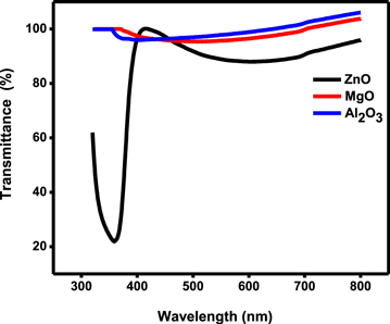
Figure 1. The transmittance spectrum of the TMO thin films prepared by a sputtering technique.
Download figure:
Standard image High-resolution imageFigure 2 shows the refractive index v/s wavelength spectrum of TMO ARCs. The refractive index of ZnO was higher compared to MgO and Al2O3 in all the wavelength regions studied. The ZnO layers refractive index 2.22 was higher at a lower wavelength of 245 nm and almost became constant after 645 nm before reducing to 1.94. The film thickness for ZnO was 83.2 nm and matches well with an expected value. Similarly, the MgO thin films exhibit the same behavior with a refractive index ranging in between 1.84 to 1.68 and thickness around 93.6 nm. However, the refractive index of Al2O3 thin film increases from 250 nm to 290 nm and decreases with increasing wavelength with a refractive index between 1.77 and 1.44. The variation of the refractive index in Al2O3 thin film is mainly due to its amorphous nature which is confirmed in XRD studies. The film thickness was around 82.2 nm and almost matches the values obtained from cross-section SEM. Refractive index values obtained for ZnO and Al2O3 are nearly the same and are in good agreement with the literature [17, 18].
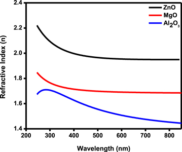
Figure 2. The wavelength-dependent refractive index spectrum of TMO ARCs.
Download figure:
Standard image High-resolution imageThe x-ray diffraction (XRD) pattern of ZnO thin film grown on the glass substrate is shown in figure 3. The XRD peaks very well matches with the standard PDF values (JCPDS, 36–1451) [19]. The intensity of the (002) peak was observed to be very strong in comparison with another peak (103). On the basis of the XRD results, we conclude that the prepared ZnO thin film is highly crystalline in nature with a hexagonal wurtzite structure. The XRD pattern is also of a single phase with no other secondary phase. Figure 3 also includes the XRD pattern of the MgO thin film sputtered on the glass substrate. Peaks identified in the spectrum at 2θ = 35.08°, 42.99°, and 62.90° can be indexed to (111), (200), and (220) reflections from strongly crystallized MgO. All the diffraction peaks can be indexed as cubic MgO and well matches with JCPDS 01–1235 [20]. Figure 3 also shows the XRD patterns of Al2O3 deposited films. The α-Al2O3 phase of the Al2O3 could be confirmed by the strong reflection peak at (0 2 4) in the deposited Al2O3 thin film. The formation of α-Al2O3 is due to transformation of alumina from δ–α phase, which also indicates insufficient reaction time for complete conversion [21].
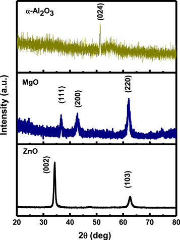
Figure 3. The XRD pattern of TMO thin film grown on the glass substrate.
Download figure:
Standard image High-resolution imageThe composition and chemical state investigation of TMO ARC film surfaces were studied by x-ray photoemission spectroscopy (XPS) and shown in figure 4. The asymmetric peak observed at low binding energy 530. 6 eV in the O1s region for an as-prepared ZnO sample corresponds to O2 ions in a normal ZnO wurtzite structure. The chemical state of Zinc in the ZnO thin film was confirmed by observing the Zn 2p core-level peaks at 1014 eV, 1022 eV and Auger Zn LMM peak 472 and 493 eV. Our values obtained for ZnO spectrum is consistent with the values reported earlier [22]. The XPS spectra of MgO thin film also shows that the peak observed at 529.27 and 972.72 eV corresponds to O2 ions whereas the peaks corresponding to Mg2+ 2p and Mg2+ 2 s was observed at 34.82, 61.57 and 458 eV respectively. Apart from these, no metal impurity or adsorption trace were observed, confirming that the sample composition of Mg and O. When compared with the Mg atom 2p level (∼49.8 eV) to earlier reported literature, it can be deduced that the Mg exists in a single chemical state throughout the growth process establishing its oxidation [23].
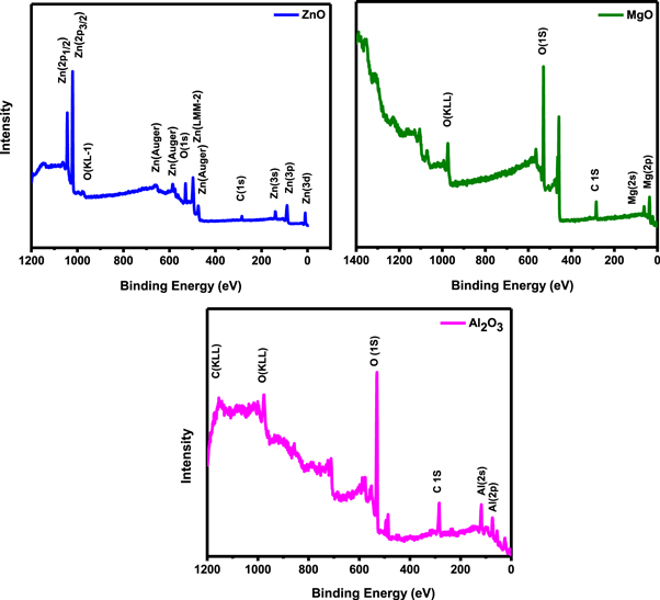
Figure 4. The XPS spectrum of TMO thin film grown on the glass substrate.
Download figure:
Standard image High-resolution imageSimilarly, the XPS spectrum of Al2O3 thin film confirms the presence of chemical composition Al, O, C with a major contribution of Al, O and minor contribution of C. The presence of carbon is due to contamination during the sputtering process. The peaks observed at binding energies of ∼73.03 eV, 118.34 eV, 284.67 eV, 531.49 eV, 975 eV, and 115 eV are associated with the chemical element states of Al 2p, Al 2 s, C 1 s, O KLL and C KLL respectively. Several authors have reportedly found two peaks corresponding to O 1 s and peroxide at B.E = 530.5 and 532–533.5 eV, respectively. The O1s symmetric peak at 531.2 and 530.5 eV without any shoulder might arise from their growth procedures or conditions [24].
Figure 5 shows the top surface scanning electron microscope (SEM) image of TMO sputtered ARC films. Image taken at different magnifications on glass substrate reveals densely packed microstructure with widely and evenly distributed grains on the surface. The closer inspection of the top surface reveals that the grains are not considerably distinct. However, the clusters of grains are of indefinite shape formed due to lower substrate temperature during the sputtering of films. An earlier report suggests that the heat treatment at elevated temperature yields significant grain growth for metal oxides post-deposition [25]. Nevertheless, high- temperature treatment may disturb the device structure.

Figure 5. Top surface SEM images of TMO thin film grown on the glass substrate.
Download figure:
Standard image High-resolution imageCross-section SEM micrograph of all the TMO films showed compact, homogeneous nature and perfectly adherent grains to the substrate (figure 6). Furthermore, the film thicknesses observed in the cross-sections images are in good agreement with the values obtained by ellipsometry and satisfy the conditions to be used as ARC in a photovoltaic device, as discussed earlier. The thickness of ZnO and MgO, as measured from SEM cross-section was around 77 nm and 90 nm whereas it was around 79 nm for Al2O3 thin films.

Figure 6. Cross-section SEM images of TMO thin film grown on the glass substrate.
Download figure:
Standard image High-resolution imageThe basic photovoltaic (PV) device parameters extracted with and without ARC device are shown in the figure 7 and the corresponding parameters are given in table 1. In order to measure the efficiency, the open-circuit voltage (Voc), short circuit current (Isc) and fill factor (FF) were measured [25] with reference to 1 sun power input (Pin).

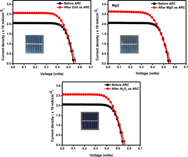
Figure 7. JV characteristics of devices extracted from solar simulator before and after ARC deposition.
Download figure:
Standard image High-resolution imageTable 1. Parameters obtained from solar simulator before and after ARC deposition on solar cells.
| Device | Voc (Voths) | Isc (Amps) | Jsc (mA/cm2) | I max (Amps) | Vmax (volts) | Power max | Fill factor | Efficiency (%) | |
|---|---|---|---|---|---|---|---|---|---|
| Device before ARC | 1 | 0.546 | 0.021 | 20.578 | 0.0199 | 0.433 | 8.289 | 73.782 | 8.289 |
| 2 | 0.547 | 0.0208 | 20.756 | 0.0193 | 0.436 | 8.328 | 73.358 | 8.328 | |
| 3 | 0.547 | 0.021 | 20.814 | 0.0194 | 0.432 | 8.380 | 73.621 | 8.380 | |
| Device after ARC | 1-Zno | 0.564 | 0.026 | 25.656 | 0.023 | 0.412 | 9.633 | 66.603 | 9.633 |
| 2-MgO | 0.571 | 0.027 | 26.455 | 0.024 | 0.404 | 9.865 | 64.064 | 9.864 | |
| 3-Al2O3 | 0.562 | 0.026 | 26.484 | 0.024 | 0.393 | 9.125 | 61.225 | 9.125 |
Initially, the efficiency of the device without ARC was measured under the optimum condition of 1 sun and the conversion efficiency was between 8.28 to 8.38%.
From table 1, it is clear that the solar cell with ARC has shown the enhanced photovoltaic performance in all three devices. The short circuit current Jsc of reference cell was 20.57 mA cm−2 whereas it increased to 25.65 mA cm−2 after ZnO deposition as ARC. This consequently gives a maximum cell efficiency of 9.63% against 8.28% to the reference cell. Thus, ZnO antireflection coating contributes to the enhancement of efficiency by 1.35%. Similar behavior was observed in MgO deposited cell. Jsc of MgO as ARC was 26.45 mA cm−2 compared to the reference cell having 20.75 mA cm−2. The efficiency of the cell increased from 8.32% to 9.8%.
The Jsc of Al2O3 was 26.48 mA cm−2 compared to reference cell value of 20.81 mA cm−2 this resulted to increase in efficiency from 8.38% to 9.12%. Though the Jsc of the MgO coated device was more compared to other cells with ARC, the fill factor of the cell with ZnO was notably high compared to the former as clear from table 1. One possible reason for the increase in Jsc for MgO is an increase in shunt pathways created due to ARC. According to these results, the improvement in the efficiency of solar cells is mainly attributed to the increase in the short circuit current due to the reduction of reflectivity from the front surface and the enhancement of light transmission by anti-reflective layer which results in the generation of more charge carriers in the device.
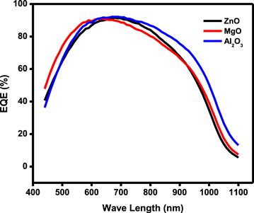
Figure 8 shows the EQE v/s wavelength of the devices with ARC. For a wavelength range between 450 and 680 nm, it is noted that the external quantum efficiency increases for all the devices ∼92% and the Al2O3 exhibits higher EQE with the higher antireflection layer. This increase is explained by the fact that in these wavelength ranges of the solar spectrum the material is more absorbent and thus the incident photon energy is greater than the gap of silicon. For a wavelength range between 680 and 1100 nm, the rapid visible and progressive decline are noted in spectral response due to very low absorption of incident light with photon energies close to the gap of silicon [26].
Figure 8. The EQE v/s wavelength after ARC on device.
Download figure:
Standard image High-resolution image
4. Conclusion
In the current study on the fabrication of Si-based solar cells, a comprehensive study on device performance has confirmed the improvement in device performance post-deposition of ZnO, MgO, and Al2O3 as ARC layers. The top surface SEM micrograph of RF-sputtered ZnO, MgO, and Al2O3 thin films showed a compact and smooth surface without any pits or porosity with grain size in the order of a nanometer. Ellipsometry measurement of refractive index as a function of wavelength showed a higher value of the refractive index for all ARCs as compared to glass. Transmittance measurement of ARCs as a function of wavelength showed that the films were transparent in the visible region and decreases in lower wavelength regions. This decrease of transmittance is due to absorption of light which excites electrons from the valence band to the conduction band.
XRD pattern of ARCs showed phase pure structure without any other impurity peaks. The coating thickness measured from cross-section SEM of ARCs was compatible with the refractive index of the silicon wafer and the consequent device structure which has greatly influenced the conversion efficiency of the device. XPS spectra of the ZnO, MgO, and Al2O3 of as-grown films show the standard peaks corresponding to the core level binding energies.
Illuminated J-V measurement of the devices has shown an increase in the short circuit current in all the devices with ARC as compared to the reference device. Consequently, the ZnO antireflection coating contributed to an enhancement of efficiency by 1.34% whereas MgO coated cell efficiency increased to 9.64% compared to the reference device with an efficiency of 8.33%. Similar behavior was observed in Al2O3 deposited cells with an increase in efficiency from 8,38% to 9.12%. In all the ARC coated devices the conversion efficiency of solar cells is mainly attributed to the increase in a short circuit current. This increase in short circuit current is due to the reduction of reflectivity from the front surface and the enhancement of light transmission by antireflective layer contributing to generate more charge carriers in the device. The quantum efficiency of the device with ZnO as ARC was 91% at 670 nm whereas MgO coated device exhibited the efficiency of 90% at 678 nm and 92% at 672 nm for Al2O3 respectively. The loss of quantum efficiency in longer wavelengths may be due to the non-optimal thickness of the photo absorber layer deposited in the fabricated devices [27].
Acknowledgments
Author (RS) gratefully acknowledges Vision Group of Science and Technology (VGST), Dept. of IT, BT and S&T, Govt. of Karnataka, India for the project grant of CESEM, vide GDR No.221 dated 24–02–2014 for the Dept of Physics, MITE Moodbidri. This research was performed using facilities at CeNSE, Indian Institute of Science (IISc), Bangaluru, funded by the Ministry of Electronics and Information Technology (MeitY), Govt of India. Acknowledgment is also to Mr Rajesh Chouta, Chairman, Mangalore Institute of Technology & Engineering, Moodbidri, for extending the research facility and coordinating the laboratory visits to accomplish research work.