

Abstract
In this paper, a comparative study of Mn3O4/PbS and CuO/PbS composites deposited by chemical bath deposition (CBD) method has been made using x-ray diffraction (XRD), Scanning electron microscope (SEM), Rutherford backscattering (RBS), UV–vis spectroscopy and four point probe techniques. Structure of both composites were observed by XRD technique. The crystallite size for Mn3O4/PbS and CuO/PbS polycrystalline films were found to be 34.86 nm and 19.14 nm respectively. The surface morphology of both composites were observed by SEM technique. Mn3O4/PbS films showed non-uniform irregular spherical particles spread across the substrate surface, whereas CuO/PbS thin films showed uniform grains with dense structure which are well covered to the substrate with rod like structure. Both films have high absorbance exhibiting a maximum in the UV region. The direct band gaps of 3.90 eV and 3.95 eV were observed for Mn3O4/PbS and CuO/PbS films respectively. The wide band gap values are in the range suitable for use as window materials in solar cell fabrication and high frequency applications.
Export citation and abstract BibTeX RIS
Introduction
In recent years, semiconductor nanocrystalline films have been widely investigated due to the novel size dependent properties [1]. The main advantage of using nanomaterial is that it consists of very small particles. As they are small, nanostructures can be packed very closely together. As a result, on a given unit area one can locate more functional nanodevices, which is very important for nanoelectronics [2]. Their high packing density has the potential to bring high area and volume capacity to information storage and higher speed of information processing [3]. In view of technical applications, the optical properties of nanoparticles and nanocomposites are of major interest. Besides their economic, the scientific background of these properties is of fundamental importance in order to understand the behaviour of nanomaterials [4].
The survey of literature showed that the synthesis of core/shell heterostructures has gained recognition due to the synergetic properties or complementary behaviours offered by the composite nanostructures. There are many studies on the synthesis of various core/shell heterostructures such as semiconductor/semiconductor [5], semiconductor/metal [6], metal/metal oxide [7], metal/metal [8], metal oxide/metal oxide [9], metal oxide/conductive polymer [10] have been explored, and enhanced properties have been demonstrated. However, research work on oxide/sulphide core–shell thin films is limited [11–15]. In our previous work, we studied the effect of annealing temperature on the structural, optical and solid state properties of Mn3O4/PbS and CuO/PbS double layer thin films [16, 17]. Here, we report on the comparative investigation of the structural, optical and solid state properties of Mn3O4/PbS and CuO/PbS composite films deposited on plane glass substrates using chemical bath deposition technique.
Experimental
The chemical bath for the deposition of Mn3O4 was made up of a mixture of 12 ml of 1 M MnCl4, 12 ml of 1 M NH4Cl, 12 ml of 100% NH3 and 24 ml of water. Five (5) clean glass slides were then inserted vertically into the solution. The deposition was allowed to proceed at temperature of 80 °C for 5 h after which the coated substrates were removed, washed with distilled water and allowed to dry. The deposited Mn3O4 was inserted in a mixture containing 5 ml of 0.2 M Pb(NO3)2, 5 ml of 1 M SC (NH2)2, 5 ml of 1 M NaOH and 35 ml of distilled water put in that order in 100 ml cleaned and dried beaker for 50 min to form Mn3O4/PbS core–shell thin film. One sample each of the deposited films was selected for characterization.
The chemical bath for the deposition of CuO was made up of a mixture of 4 ml of 1 M CuSO4, 4 ml of 1 M KCl, 2 ml of 100% NH3 and 13 ml of distilled water. The deposition took place at 80 °C bath temperature for 3 h. To deposit CuO/PbS films, the deposited CuO films were inserted into a mixture containing 5 ml of 0.2 M Pb(NO3)2, 5 ml of 1 M SC (NH2)2, 5 ml of 1 M NaOH and 35 ml of distilled water put in that order in 50 ml beaker for 50 min.
Optical absorption data were obtained with a thermo scientific GENESYS 10 S model UV–vis spectrophotometer at normal incidence of light in the wavelength range of 300–1000 nm. Proton Induced x-ray Emission (PIXE) scans on the samples from a Tandem Accelerator Model 55DH 1.7 MV Pellaton by National Electrostatic Corporation (NEC), USA which effectively performed Rutherford Back Scattering (RBS) elemental characterizations on both deposits and substrates. The RBS also deciphered the thicknesses of film deposits. The crystal structure and phase analysis of the deposited film was carried out at room temperature with an x-ray diffractrometer Rigaku Ultima IV model, using gracing incident at 30 mA, 40 KV with CuKα radiation of wavelength λ = 0.154 06 nm. Scanning Electron Micrscope (Tescan model) was used to observe the morphology of the deposited composites thin films.
Results and discussion
The grown composites thin films were characterized by powder x-ray diffractometer. Figure 1 shows the x-ray diffraction spectra of Mn3O4/PbS and CuO/PbS composite thin films. The strong peak intensity indicates the high degree of crystallinity of the films. The presence of more than one peak indicates that both films are polycrystalline. Different diffraction patterns can be observed for both composites. Comparative study of the XRD patterns of both films showed that Mn3O4/PbS films exhibited more intense peaks compared to CuO/PbS films. The average grain sizes of 34.86 nm and 19.14 nm were observed for Mn3O4/PbS and CuO/PbS films respectively. The micro strain of both films which is related to the lattice misfit and depends on the deposition conditions was calculated as 0.1020 and 0.1039 for Mn3O4/PbS and CuO/PbS films respectively. The peaks at 2θ values of 25.964°, 30.075°, 43.059° and 50.978° are attributed to galena PbS (JCPDS 00-005-0592). These were assigned to the diffraction line produced by (111), (200), (220) and (311) planes. The peaks at angles of 18°, 32.316°, 36.450° and 50.710° are identified to be hausmannite Mn3O4 (JCPDS 00-024-0734) and are assigned diffraction lines produced by (101), (103), (202) and (105) planes. However, additional peaks of 28.082°, 29.615° and 30.645° are identified to be Pb2MnO4 (JCPDS 00-036-0844) phase and assigned diffraction lines produced by (131), (330) and (231) planes while peak of 35.583° corresponds to (212) plane of Copper hydroxide sulphate phase (JCPDS 00-011-0653).

Figure 1. XRD patterns of Mn3O4/PbS and CuO/PbS composites thin films.
Download figure:
Standard image High-resolution imageThe average crystallites sizes D in both composites was deduced from the scherrer's equation [18, 19].

The microstrain (ε) produced in the composites was calculated using the equation below [20].

Where  is the peak width at mid height, θ is the diffraction angle, K is a constant and is equal to 0.9, the constant
  = 0.15406 nm, D is the grain size and ε represent strains in the film.
The SEM images of Mn3O4/PbS and CuO/PbS composites thin films are shown in figures 2 and 3 respectively. Figure 2 depicts non-uniform irregular spherical grains scattered across the substrate surface with few pinholes while figure 3 shows particles engaged in a flower-like rod structure indicating the nanocrystalline nature of CuO/PbS thin films. The observed long network of structure ordering makes the CuO/PbS film good material for design of light-trapping configuration for solar cells [21].

Figure 2. SEM images of Mn3O4/PbS composite thin films.
Download figure:
Standard image High-resolution image
Figure 3. SEM images of CuO/PbS composite thin films.
Download figure:
Standard image High-resolution imageThe elemental composition of the films was carried out using Rutherford backscattering technique. The percentage elemental composition of Mn3O4/PbS and CuO/PbS composites thin films are presented in tables 1 and 2 respectively. The thicknesses of the films as deciphered by RBS are 1026 nm and 650 nm for Mn3O4/PbS and CuO/PbS films respectively. The equation below [22] was also used to calculate the thickness of the film in order to compare with that deciphered by RBS technique. The calculated thicknesses are 1067 nm and 698 nm for Mn3O4/PbS and CuO/PbS films respectively. The calculated thicknesses of Mn3O4/PbS and CuO/PbS films are in conformity with the RBS results. The RBS micrographs of Mn3O4/PbS and CuO/PbS thin films are shown in figures 4 and 5 respectively.

Where t is thickness, no is the refractive index of the medium of the incident light, which in this study is air, ng is the refractive index of the substrate (glass in this case); and n is the refractive index of the thin film, R is reflectance and λ is wavelength.
Table 1. Percentage elemental composition of Mn3O4/PbS composite thin films.
| Sample | Pb | Fe | Mn | Ca | K | S | Si | Al | Na | O |
|---|---|---|---|---|---|---|---|---|---|---|
| Glass Slide | — | 0.30 | — | 6.00 | 3.50 | — | 34.00 | 5.20 | 25.00 | 26.00 |
| Mn3O4/PbS | 70.63 | — | 17.78 | — | — | 29.33 | — | — | — | 82.22 |
Table 2. Percentage elemental composition of CuO/PbS composite thin films.
| Sample | Pb | Cu | Fe | Ca | K | S | Si | Al | Na | O |
|---|---|---|---|---|---|---|---|---|---|---|
| Glass Slide | — | — | 0.30 | 6.00 | 3.50 | — | 34.00 | 5.20 | 25.00 | 26.00 |
| CuO/PbS | 0.59 | 5.64 | — | — | — | 33.16 | — | — | — | 94.36 |

Figure 4. RBS micrograph of Mn3O4/PbS composite thin film.
Download figure:
Standard image High-resolution image
Figure 5. RBS micrograph of CuO/PbS composite thin film.
Download figure:
Standard image High-resolution imageThe optical absorption and transmission spectra of Mn3O4/PbS and CuO/PbS composites deposited on transparent glass recorded in wavelength range 300–1000 nm are shown in figures 6 and 7 respectively. Mn3O4/PbS film exhibited peak absorbance of about 1.40 (a.u) whereas CuO/PbS exhibited peak absorbance of about 1.70 (a.u). Both peaks occur in the UV region. A significant difference in the absorption peak is observed. The absorption edge for Mn3O4/PbS films occurred at about 0.40 (a.u) corresponding to about 318 nm whereas CuO/PbS films exhibited absorption edge at about 0.65 (a.u) corresponding to about 314 nm. The absorbance of both films are higher in the UV region with a sharp decrease in the visible and near infrared regions. The absorbance of CuO/PbS composite is generally higher in the UV region compared to Mn3O4/PbS composite. From figure 8, Mn3O4/PbS films transmit more than CuO/PbS films in the UV region. However, in the visible and infrared regions, CuO/PbS films transmit higher than Mn3O4/PbS films. Generally, Mn3O4/PbS composite transmit below 50%, whereas CuO/PbS composite transmit above 50%. Figure 9 depicts the plots of reflectance against wavelength for Mn3O4/PbS and CuO/PbS composites thin films. It is observed that the reflectance of both films vary in similar manner. However, Mn3O4/PbS composite films shows higher reflectance in the entire electromagnetic region compared to CuO/PbS composite films.
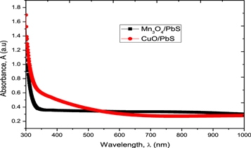
Figure 6. Optical absorbance of Mn3O4/PbS and CuO/PbS composite thin films.
Download figure:
Standard image High-resolution image
Figure 7. Optical transmittance of Mn3O4/PbS and CuO/PbS composites films.
Download figure:
Standard image High-resolution image
Figure 8. Reflectance (R) against wavelength of Mn3O4/PbS and CuO/PbS composites films.
Download figure:
Standard image High-resolution image
Figure 9. Plots of absorption coefficient as a function of photon energy.
Download figure:
Standard image High-resolution imageThe transmittance (T), reflectance (R), absorption coefficient (α) and band gap (Eg) were calculated from the following relations [23]:


Where A is band edge parameter and value of n determines the nature of optical transition (n = ½ indicates direct transition and n = 2 indicates indirect transition).
The plots of absorption coefficient as a function of photon energy for both composites are presented in figure 9. The absorption coefficients of Mn3O4/PbS and CuO/PbS composites films vary in a similar manner, increasing from 0.75 × 10⁶ m−1 at 1.23 eV to a maximum of 2.75 × 10⁶ m−1 at 4.25 eV for Mn3O4/PbS composite films, and 1.1 × 10⁶ m−1 at 1.23 eV to a maximum of 6.25 × 10⁶ m−1 at 4.25 eV for CuO/PbS composite films. In general, Mn3O4/PbS composite films exhibited lower absorption coefficient values compared to CuO/PbS composite thin films. The absorption coefficients of both films increased with increasing photon energy (decreasing wavelength).
Figure 10 depicts the plots of the product of absorption coefficient and photon energy square (αhν)2 against photon energy (hv). The extrapolation of straight line portion of (αhν)2 against hv to energy axis for zero absorption coefficient gave optical band gap energy value as 3.90 eV and 3.95 eV for Mn3O4/PbS and CuO/PbS composites respectively. Values for Mn3O4 as widely reported is 3.07–3.55 eV [24, 25] while that of CuO is 1.90–2.91 eV [26, 27]. It can be seen that the formation of Mn3O4/PbS and CuO/PbS composites films shifted the fundamental absorption edge of core binary origin, thus providing tuning effect to the band gap for special applications. The primary function of a window layer in a heterojunction as contained in the literature is to form a junction with the absorber layer while admitting a maximum amount of light to the junction region and the absorber layer. The wide direct band gaps of the films placed them as suitable materials for window layers in solar cell fabrication.

Figure 10. Plots of (αhν)2 against photon energy (hv) for Mn3O4/PbS and CuO/PbS composites films.
Download figure:
Standard image High-resolution imageThe refractive index (n), extinction coefficient (k), optical conductivity (σo), real dielectric constant ( ), imaginary dielectric constant (
 ), electrical conductivity (σe) and thermal conductivity (σt) were calculated using the relations available in literature [28, 29].


Figure 11 shows the plots of refractive index as a function of photon energy for Mn3O4/PbS and CuO/PbS composites thin films while figure 12 depicts the extinction coefficient plots against photon energy. From figure 11, we observed that the refractive index increased with increasing photon energy (decreasing wavelength) with a sharp decrease at 3.75 eV and 3.00 eV for Mn3O4/PbS and CuO/PbS composites respectively. The extinction coefficients of both films vary in the same manner in the VU and infrared regions. However, different behaviour is observed in the visible region. It decreased with photon energy in the visible region for Mn3O4/PbS film, whereas it increased with photon energy in the same region for CuO/PbS films. Generally, Mn3O4/PbS composite films showed lower values of extinction coefficients compared to CuO/PbS composite thin films.

Figure 11. Plots of refractive index (n) against photon energy (hv) for Mn3O4/PbS and CuO/PbS composites.
Download figure:
Standard image High-resolution image
Figure 12. Plots k against (hv) for Mn3O4/PbS and CuO/PbS composites thin films.
Download figure:
Standard image High-resolution imageThe plots of optical conductivity as a function of photon energy (figure 13) shows that Mn3O4/PbS and CuO/PbS composites films behaviour differently in the infrared region. i.e it increased with photon energy for Mn3O4/PbS composite films, whereas it decreased with photon energy for CuO/PbS composite films. However, in UV and visible regions, both films exhibited similar behaviour. We observed that the real dielectric constant (figure 14) and refractive index (figure 11) vary in a similar manner with photon energy. Such behaviour has been reported by other authors [22, 30–32]. The imaginary dielectric plots as a function of photon energy is shown in figure 15. Mn3O4/PbS films has higher values of imaginary dielectric compared to CuO/PbS films. However, both films showed similar behaviour in the UV and infrared regions. Figure 16 depicts the plots of thermal conductivity as a function of photon energy of Mn3O4/PbS and CuO/PbS composites thin films. Both films exhibited similar behaviour across the entire spectrum reaching a maximum in the UV region. An increasing trend of thermal conductivity with increasing photon energy (decreasing wavelength) was observed for both films.

Figure 13. Plots of optical conductivity against photon energy.
Download figure:
Standard image High-resolution image
Figure 14. Plots of real dielectric constant ( ) against photon energy (hv).
Download figure:
Standard image High-resolution image
Figure 15. Plots of real dielectric constant ( ) against photon energy (hv).
Download figure:
Standard image High-resolution image
Figure 16. Plots of thermal conductivity against photon energy (hv).
Download figure:
Standard image High-resolution image
Conclusion
Mn3O4/PbS and CuO/PbS composites thin films were successfully coated on the glass substrate using chemical bath deposition technique. The structural, morphological, optical and solid state properties of the prepared films were analyzed. Both composites varied considerably with the structural, morphological, optical and solid state parameters. Both composites are semiconductors with different wide direct band gaps suitable for use as window materials in heterojunction solar cell, optoelectronic devices and high frequency applications.